Spin diode based on a single-wall carbon nanotube
Abstract
Electronic transport through a single-wall metallic carbon nanotube weakly coupled to one ferromagnetic and one nonmagnetic lead is analyzed in the sequential tunneling limit. It is shown that both the spin and charge currents flowing through such systems are highly asymmetric with respect to the bias reversal. As a consequence, nanotubes coupled to one nonmagnetic and one ferromagnetic lead can be effectively used as spin diodes whose functionality can be additionally controlled by a gate voltage.
pacs:
72.25.Mk, 73.63.Kv, 85.75.-d, 73.23.HkSince their discovery, ijima carbon nanotubes (CNTs) have been extensively studied from both fundamental and application points of view. saito98 ; anantram06 Owing to extreme flexibility of nanotubes (they can be either metallic or semiconducting), they have turned out to be ideal natural systems to study one-dimensional electronic transport in various transport regimes. saito98 ; anantram06 Transport characteristics of a CNT contacted to metallic leads depend on the strength of CNT-leads coupling. babic For very good coupling, transport reveals features typical for electron waveguides. In turn, for weak coupling between the nanotube and leads, CNT behaves as a large quantum dot with many orbital levels participating in electronic transport. liangPRL02 In the intermediate case and at sufficiently low temperatures, transport reveals features characteristic of the Kondo phenomenon. nygard00 When the leads are additionally ferromagnetic, transport properties of a CNT depend on the relative orientation of the leads’ magnetic moments, leading to the so-called spin-valve effect. tsukagoshi99 ; zhao02 ; sahoo05 ; manPRB06 ; nagabhiravaAPL06 ; cottetPRB06 ; schonenberger06 ; weymannPRB07 Very recently Merchant and Markovic markovic07 observed strong diode-like behavior in transport characteristics of a CNT coupled to two metallic leads, one being ferromagnetic (Co) and the second one nonmagnetic (Nb). Motivated by this experiment, in this Letter we analyze theoretically transport through a single-wall metallic carbon nanotube weakly coupled to one ferromagnetic and one nonmagnetic lead, and show that indeed such systems reveal features which are typical of spin diodes. By considering transport in the sequential tunneling regime, we show that both the spin and charge currents become strongly asymmetric with respect to the bias reversal. The magnitude and sign of this asymmetry depends on the bias voltage, and can be additionally controlled by a gate voltage, which is of particular interest from the application point of view. It is also worth noting that a similar spin diode behavior has been predicted for single semiconducting quantum dots. rudzinskiPRB01 ; souzaPRB07
To describe the spin-diode features in transport characteristics, we consider the system consisting of a single-wall metallic CNT which is weakly coupled to one nonmagnetic (left) and one ferromagnetic (right) lead. Hamiltonian of the system has the general form, . The first two terms describe noninteracting electrons in the leads, , for the left () and right () leads, with being the energy of an electron with the wave vector and spin in the lead . To describe the CNT in the weak coupling limit we employ the model Hamiltonian introduced in Ref. oregPRL00 ,
| (1) | |||||
where , and . The th discrete energy level in the subband (), , is given by , where is the spacing between levels following from quantization in a particular subband, and is the energy mismatch between the level sets corresponding to the two subbands. The charging energy of the nanotube is denoted by and is the charge induced by the gate voltage. The additional Coulomb energy of two electrons in the same level is described by , while is the exchange parameter.
The tunneling Hamiltonian reads , where is the tunnel matrix element between the lead and the th level. Coupling of the th level to external leads can be described by , where is the density of states in the lead for spin . Defining the spin polarization of the ferromagnetic electrode as , one can write the coupling of CNT to the right lead as for the majority (minority) electrons, while coupling to the nonmagnetic left lead as (for all levels ). Since CNT may be coupled to electrodes with different coupling strengths, we introduce an asymmetry factor , and assume (coupling of CNT to the ferromagnetic electrode is weaker than to the nonmagnetic one).
When the CNT is weakly coupled to external leads, current flows due to the sequential tunneling processes, except the Coulomb blockade regions, where cotunneling processes dominate over the sequential ones. However, both sequential and cotunneling contributions to the current in the Coulomb blockade are small in comparison to the sequential current out of the blockade regime. The latter regime is of particular interest from the application point of view and is relevant to many recent experiments. Therefore, we restrict the following considerations to the sequential transport regime, and use the real time diagrammatic method limited to the first-order expansion. Tunneling rates in the sequential approximation are given by the usual Fermi golden rule. In turn, the occupation probabilities can be calculated from the master equation , thielmann ; weymannPRB07 where is the vector containing the occupation probabilities, and is a many-body state of the CNT. The elements of matrix are given by , with , for , and , where and is the electrochemical potential in the lead . The first (second) term in the bracket describes tunneling to (from) the nanotube from (to) the lead . Apart from this, one arbitrary row of matrix has been replaced by due to the normalization condition . The sequential current flowing through the nanotube can be then calculated from the formula , thielmann ; weymannPRB07 where the elements of matrix are given by , with being the number of electrons in state and denoting the Heaviside function.
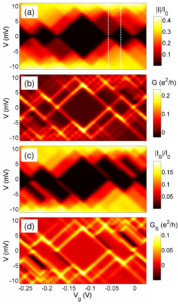
In order to model the single-wall metallic carbon nanotube we have taken the parameters derived from the experiments of W. Liang et al. liangPRL02 We have also introduced a conversion factor, , which relates the gate voltage to the electrochemical potential shift. grabert92 In Fig. 1 we show density plots of the absolute value of the current , differential conductance , absolute value of the spin current , and the differential spin conductance , calculated as a function of the gate and bias voltages. The spin current is defined as , where is the current flowing in the spin- channel. is related to the angular momentum current by the relation . Due to periodicity, in Fig. 1 we show only one sequence of the four-fold shell filling structure of single-wall CNTs. First of all, the Coulomb blockade regions are clearly visible – see the large and small black diamonds in Fig. 1(a). We also point on the inverse symmetry of the transport characteristics shown in Fig. 1 with respect to the center of the large blockade diamond.
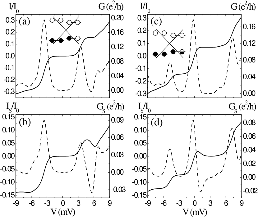
In Fig. 2 we show the bias voltage dependence of the transport characteristics (charge and spin currents and the corresponding differential conductances) for different values of the gate voltage, V and V, respectively. These characteristics correspond to the vertical cross-sections of Fig. 1 through the center of the first small diamond to the right of the large one, and to the resonance point between the large and small diamonds, respectively, see the dotted lines in Fig. 1(a). We recall that the large diamond corresponds to the situation when the sequence of the four electronic levels of the CNT becomes filled with four electrons, while the first small blockade diamond to the right of the large one corresponds to the situation when these four-level sequence is occupied by three electrons only. In turn, the first small diamond to the left of the large one describes the situation when the next four-fold level-sequence is occupied by a single electron. liangPRL02 ; weymannPRB07
As can be seen in the figures, the current flowing through the system is not symmetric with respect to the bias reversal. This is associated with the asymmetry in bare tunneling matrix elements for the spin-majority and spin-minority electrons between the CNT and ferromagnetic lead. Due to this spin-dependence, tunneling processes involving the spin-majority electrons are faster than those involving the spin-minority ones. On the other hand, the matrix elements for tunneling between the nonmagnetic lead and the nanotube do not depend on the spin orientation. Due to the spin dependence of tunneling processes, charge current is associated with a nonzero spin current flowing through the system. Spin current, similarly as the charge current, also reveals features typical of spin-diode, see Fig. 2(b) and (d). Thus, carbon nanotubes when coupled to one nonmagnetic and one ferromagnetic lead can be used as spin diodes, and their functionality can be controlled additionally by a gate voltage, see Fig. 1.
Let us now look more carefully at the two various situations shown in Fig. 2. In Fig. 2(a,b) we show the bias dependence of the transport characteristics for the gate voltage corresponding to the Coulomb blockade region with three electrons in the last level-sequence of the CNT. We recall, that for the parameters assumed, electrons tunnel much easier through the barrier between the CNT and nonmagnetic lead than through the barrier between CNT and ferromagnetic lead. At small bias the system is in the blockade regime and current starts to flow (for both bias polarization) when the bias voltage exceeds a threshold. grabert92 For positive voltage electrons tunnel from the ferromagnetic lead to the nonmagnetic one. In Fig. 2 for V the step in current for positive bias is smaller than that for negative one. This can be explained by taking into account spin asymmetry in tunneling matrix elements, and difference in barriers between the left and right leads (barrier between the magnetic leads and CNT is larger). For positive bias transport goes mainly through the states (lowest level doubly occupied and the next one occupied by a spin-up electron) and (the lowest level doubly occupied and the next one empty). In other words, an electron leaves first the CNT and tunnels to the nonmagnetic lead, and then a spin-up electron from the magnetic lead tunnels to the CNT. For negative bias, in turn, transport takes place via states (both levels of the sequence are doubly occupied) and or (one of the two levels is doubly occupied and the second one is occupied by a spin down electron). Now, an electron tunnels first to the CNT and then a spin up electron, either from the lower or from the higher level, tunnels to the magnetic lead. Thus, there are now two channels for tunneling from the CNT to the magnetic lead, which makes the step in current at the threshold large for negative bias. For positive bias there was only one channel open for tunneling so the current step was smaller. When the bias increases further, additional channel becomes open also for positive bias and the currents become comparable. However, the two plateaus above the threshold for positive and negative bias are significantly different. In addition, the asymmetry in charge current leads to the corresponding asymmetry in spin currents, see Fig. 2(b). Moreover, the asymmetry for spin current is even more pronounced than for the charge current. As the charge current varies rather monotonically with the bias voltage (positive differential conductance), the spin current for positive bias drops with increasing voltage above the threshold (negative differential spin conductance). This behavior opens a functionality range for the system as a spin diode.
Owing to the symmetry of the energy spectrum of the system, the situation is reversed when the gate voltage admits one electron on the last level-sequence ( mV in Fig. 1). Due to the corresponding particle-hole symmetry, transport for positive bias goes mainly through the states (empty levels) and or (spin up electron on one of the two levels). For negative bias, on the other hand, transport takes place via states (lower level doubly occupied) and (one spin-down electron on the lower level). Thus, now two channels open at the threshold voltage for tunneling from the magnetic lead to the CNT for positive bias, and therefore the corresponding step in current is larger than for negative bias.
Consider now the situation shown in Fig. 2(c,d). Since the system is now at resonance, there is no current blockade and the current increases immediately with applied voltage. Again both the charge and spin currents for positive bias are suppressed as compared to the currents flowing when the bias is negative. The arguments accounting for this bias-reversal asymmetry are similar as in the case of V. It is also worth to note, that in a broad voltage range the spin current for positive bias is much smaller than for negative bias, see Fig. 2(d).
We point that the spin diode behavior is observed for relatively low transport voltages. For higher voltages there are more states participating in transport and the current rectification is decreased. We also notice that the operation of the spin diode can be improved by increasing the spin polarization of the right lead. For negative bias voltage when electrons tunnel from nonmagnetic to ferromagnetic lead, once the nanotube becomes occupied by a spin-down electron the current is approximately given by , whereas for positive bias the current is . Thus, by increasing , the rectification of the current is enhanced. An ideal CNT-based spin diode could be made by connecting the nanotube to half-metallic lead, where due to the energy gap in one of the two spin subbands. In addition, the operation of the diode can be tuned by sweeping the gate voltage, see Figs. 1 and 2.
This work, as part of the European Science Foundation EUROCORES Programme SPINTRA, was supported by funds from the Ministry of Science and Higher Education as a research project in years 2006-2009 and the Foundation for Polish Science.
References
- (1) S. Iijima, Nature (London) 354, 56 (1991).
- (2) R. Saito, M. S. Dresselhaus, and G. Dresselhaus, Physical Properties of Carbon Nanotubes (London, UK: Imperial College Press, 1998).
- (3) M. P. Anantram and F. Leonard, Rep. Prog. Phys 69, 507 (2006).
- (4) B. Babić and C. Schönenberger, Phys. Rev. B 70, 195408 (2004).
- (5) W. Liang, M. Bockrath, and H. Park, Phys. Rev. Lett. 88, 126801 (2002).
- (6) J. Nygård, D. Cobden, and P. E. Lindelof, Nature (London) 408, 342 (2000).
- (7) K. Tsukagoshi, B. W. Alphenaar, and H. Ago, Nature 401, 572 (1999).
- (8) B. Zhao, I. Mönch, H. Vinzelberg, T. Mühl, and C. M. Schneider, Appl. Phys. Lett. 80, 3144 (2002).
- (9) S. Sahoo, T. Kontos, J. Furer, C. Hoffmann, M. Gräber, A. Cottet, and C. Schönenberger, Nature Physics 1, 102 (2005).
- (10) H. T. Man, I. J. W. Wever, and A. F. Morpurgo, Phys. Rev. B 73, 241401(R) (2006).
- (11) B. Nagabhirava, T. Bansal, G. U. Sumanasekera, and B. W. Alphenaara, L. Liu, Appl. Phys. Lett. 88, 023503 (2006).
- (12) A. Cottet and M-S. Choi, Phys. Rev. B 74, 235316 (2006).
- (13) C. Schönenberger, Semicond. Sci. Technol. 21, S1 (2006).
- (14) I. Weymann, J. Barnaś, and S. Krompiewski, Phys. Rev. B 76, 155408 (2007).
- (15) C. A. Merchant, N. Markovic, cond-mat/0710.2297 (unpublished).
- (16) W. Rudziński and J. Barnaś, Phys. Rev. B 64, 085318 (2001); M. Wilczyński, R. Świrkowicz, W. Rudziński, J. Barnaś, and V. Dugaev, J. Magn. Magn. Mater. 290-291, 209 (2005).
- (17) F. M. Souza, J. C. Egues, and A. P. Jauho, Phys. Rev. B 75, 165303 (2007).
- (18) Y. Oreg, K. Byczuk, and B. I. Halperin, Phys. Rev. Lett. 85, 365 (2000).
- (19) A. Thielmann, M. H. Hettler, J. König, and G. Schön, Phys. Rev. B 68, 165341 (2003).
- (20) H. Grabert and M. H. Devoret, Single Charge Tunneling, (New York, 1992).
Figure captions
Fig. 1. (Color online) The absolute values of the current (a) and spin current (c) in the units of , the differential conductance (b) and the differential spin conductance (d), calculated as a function of the bias and gate voltages. The parameters are: meV, , , , , , , , , meV, and nA.
Fig. 2. The current (solid line) and differential conductance (dashed line) (a,c), and the spin current (solid line) and spin differential conductance (dashed line) (b,d) as a function of the bias voltage for V (a,b) and V (c,d). The parameters are the same as in Fig. 1. The insets illustrate the two subbands of the nanotube with the corresponding occupations – the CNT is occupied with electrons (a) [empty (filled) circles correspond to empty (occupied) charge states], while for V (c) the occupation number fluctuates between and .