Robust single-parameter quantized charge pumping
Abstract
This paper investigates a scheme for quantized charge pumping based on single-parameter modulation. The device was realized in an AlGaAs-GaAs gated nanowire. We find a remarkable robustness of the quantized regime against variations in the driving signal, which increases with applied rf power. This feature together with its simple configuration makes this device a potential module for a scalable source of quantized current.
Single electron pumps and turnstiles transporting a well defined number of charges per cycle Averin and Likharev (1991) have attracted much interest, in particular for their potential application in integrated single-electron circuits Nishiguchi et al. (2006) and in metrology providing a direct link between time and current units Mills et al. (2006). Different approaches have been investigated, such as arrays of gated metallic tunnel junctions Geerligs et al. (1990); Pothier et al. (1992); Keller et al. (1996); Pekola et al. (2007) or semiconducting channels along which the potential can be modulated continuously Kouwenhoven et al. (1991); Shilton et al. (1996); Fujiwara et al. (2006); Blumenthal et al. (2007); Kaestner et al. (2007); Fujiwara et al. (2008). One of the main issues for applicability in metrology is to achieve a high current output simultanously with accurate charge transfer. Usually, increasing the current level by raising the frequency leads to a loss in accuracy, such that parallelization has been considered Keller (2001) as an alternative to faster driving. The stringent requirements on phase and amplitude matching of the driving signals typical for many systems, requiring cross-capacitance compensation for each gate-pair and channel only allow a few approaches to be considered for such a scalable current source. Here we investigate a non-adiabatic pumping scheme realized by modulating a single voltage parameter in the quantized regime Kaestner et al. (2007); Maire et al. (2008). We find a remarkable robustness in the driving signal which should allow the application of the pump as a building block in a scalable source of quantized current.
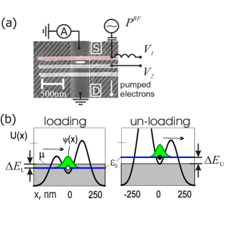
The device was realized in an AlGaAs/GaAs heterostructure. A 700 nm wide wire connected to the two-dimensional electron gas was created by etching the doped AlGaAs layer. The device was contacted using an annealed layer of AuGeNi. This channel is crossed by three Ti-Au finger gates of 250 nm separation, as shown in Fig.1(a). A quantum dot (QD) with a discrete quasi-bound state between the two upper gates is formed by applying sufficiently large negative dc voltages and to gate 1 and 2, respectively. The lowest gate was grounded and not used. An additional sinusoidal signal of power is coupled to gate 1. If the oscillation amplitude is high enough, the energy of the quasi-bound state drops below the chemical potential of the leads during the first half-cycle of the periodic signal and can be loaded with an electron from the left reservoir (see Fig1(b)). During the second half-cycle is raised sufficiently fast above to avoid backtunneling and the electron can be unloaded to the right. In this way a current is driven through the sample without an applied bias and the device acts as a quantized charge pump. For details on this pumping mechanism we refer to Ref. Kaestner et al. (2007).

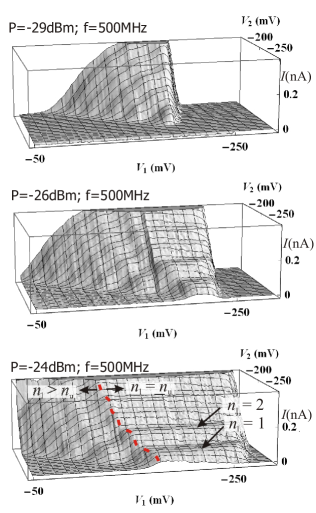
The pumped current through the unbiased device as a function of gate voltages and is shown in Fig. 2. Measurements were performed at temperature mK. Sinusoidal signals of rf-powers dBm and frequency MHz were applied to gate 1. Plateaus of different quality can be seen around the values of pA for , where on average electrons of charge per cycle are transported. To describe the behaviour qualitatively we assume that for the voltage range applied to gate 2 a high enough tunnel barrier for electrons in the drain is induced so that no electrons will be loaded from the drain. This assumption is justified since the considered voltage range lies well beyond the pinch-off voltage mV. The step-like variation of along can be explained by considering that the voltage at gate 2 determines the number of electrons loaded from the source in each cycle since it controls the dot potential during the loading phase (see also Fig. 1). In addition, it can prevent some of the captured electrons from being unloaded to the drain during the emission phase. The resulting current is determined by , where is the number of unloaded electrons to the drain. The case where occurs when is made more positive so that the rf-modulation added to is not sufficient to cause emission of all electrons over the barrier at gate 2. This explains the less pronounced steps along toward more positive values, with plateau-lengths related to the charging energy of the isolated dot: as soon as one electron is emitted to the drain the energy of the isolated dot is lowered by and might not be sufficient anymore to emit the remaining electrons over the right barrier. Tuning to more negative values will eventually lead to complete unloading of all loaded electrons to the drain, i.e. . Comparing the different plateau lengths for sufficiently large power, e.g. dBm, we conclude that for the pronounced and more extended plateau along one finds the case of . The length of this plateau is a measure of the robustness of the quantized regime in the voltage applied to gate 1.

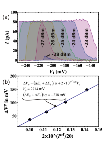
To investigate the robustness further the plateau along at is plotted in more detail in Fig. 3(a) for rf-powers and dBm. The voltage on gate 2 was set to mV. The width of the plateau increases with applied rf-power. To describe the rf-power dependence we restrict our model for simplicity to a single quasi-bound state. The energy of this state is modulated by the signal on gate 1 as , where describes the conversion from voltage to energy scale, and is the energetic offset, including a dependence on . Quantized pumping then requires complete loading of one electron exclusively from source and complete unloading exclusively to drain. In order for such a sequence to be possible the dot has to be isolated during the phase when crosses . In terms of tunneling rates to source, , and drain, , we require and for . Here is the amount of energy the quasi-bound state has to gain above in order to unload electrons to the drain. Similarly, is the energy of the quasi-bound state below before loading sets in (see Fig. 1). This means that no electrons can be captured for . Also, no electron can be emitted for . The length of the plateau can therefore be written as . The modulation amplitude is related to the power given in dBm via , where corresponds to the amplitude at mW. The linear dependence of on is confirmed experimentally and shown in Fig. 3(b). The line corresponds to mV and mV.
For future applications as a single-electron source it might also be important to determine the range of over which the QD is isolated. From bias-spectroscopy a value for meV/mV has been obtained for the QD in the open regime. Assuming the same value in the isolated regime we conclude that the QD is non-adiabatically blockaded over an energy range of more than 50 meV around .

The accuracy of this concept demonstration device has been determined at dBm and mV at the flattest part of the plateau along . The measured current pA corresponds to the theoretical value of to better than 1%. In principle, the accuracy can be improved by narrowing the channel Kaestner et al. , tuning the gate width and wafer characteristics. Estimates in Kaestner et al. have shown that for suitable choice of barrier shapes an accuracy of 1 in could in principle be achieved.
From the investigation above we conclude that the device can be conveniently implemented into a larger network where many channels are driven by the same gate. Even if the voltage signal arriving at each channel has experienced different attenuations synchronous operation is possible in the robust high-power regime. The robustness in the driving signal and its simple configuration together with the potentially high speed of tunable barrier schemes makes non-adiabatic single-parameter pumps promising candidates for an accurately quantized, large-current source as needed for fundamental experiments in metrology and quantum electronics.
Acknowledgements.
The authors acknowledge fruitful discussions with S. Amakawa and S. Lotkhov. Assistance with device fabrication from Th. Weimann, P. Hinze and H. Marx is greatly acknowledged. V.K. acknowledges financial support from the European Social Fund and the Latvian Council of Science.References
- Averin and Likharev (1991) D. V. Averin and K. K. Likharev, Mesoscopic Phenomena in Solids (Elsevier, Amsterdam, 1991), chap. Single electronics: a correlated transfer of single electrons and Cooper pairs in systems of small tunnel junctions, pp. 173 – 271.
- Nishiguchi et al. (2006) K. Nishiguchi, A. Fujiwara, Y. Ono, H. Inokawa, and Y. Takahashi, Appl. Phys. Lett. 88, 183101 (2006).
- Mills et al. (2006) I. M. Mills, P. J. Mohr, T. J. Quinn, B. N. Taylor, and E. R. Williams, Metrologia 43, 227 (2006).
- Geerligs et al. (1990) L. J. Geerligs, V. F. Anderegg, P. A. M. Holweg, J. E. Mooij, H. Pothier, D. Esteve, C. Urbina, and M. H. Devoret, Phys. Rev. Let. 64, 2691 (1990).
- Pothier et al. (1992) H. Pothier, P. Lafarge, C. Urbina, D. Esteve, and M. H. Devoret, Europhys. Lett. 17, 249 (1992).
- Keller et al. (1996) M. W. Keller, J. M. Martinis, N. M. Zimmerman, and A. H. Steinbach, Appl. Phys. Lett. 69, 1804 (1996).
- Pekola et al. (2007) J. P. Pekola, J. J. Vartiainen, M. Möttönen, O.-P. Saira, M. Meschke, and D. V. Averin, Nature Physics (2007).
- Kouwenhoven et al. (1991) L. P. Kouwenhoven, A. T. Johnson, N. C. van der Vaart, C. J. P. M. Harmans, and C. T. Foxon, Phys. Rev. Lett. 67, 1626 (1991).
- Shilton et al. (1996) J. M. Shilton, V. I. Talyanskii, M. Pepper, D. A. Ritchie, J. E. F. Frost, C. J. B. Ford, C. G. Smith, and G. A. C. Jones, J. Phys.: Condens. Matter 8, L531 (1996).
- Fujiwara et al. (2006) A. Fujiwara, H. Inokawa, K. Yamazaki, H. Namatsu, Y. Takahashi, N. M. Zimmerman, and S. B. Martin, Applied Physics Letters 88, 053121 (2006).
- Blumenthal et al. (2007) M. D. Blumenthal, B. Kaestner, L. Li, S. Giblin, T. J. B. M. Janssen, M. Pepper, D. Anderson, G. Jones, and D. A. Ritchie, Nature Physics 3, 343 (2007).
- Kaestner et al. (2007) B. Kaestner, V. Kashcheyevs, S. Amakawa, L. Li, M. D. Blumenthal, T. J. B. M. Janssen, G. Hein, K. Pierz, T. Weimann, U. Siegner, et al., arXiv:0707.0993 [cond-mat.mes-hall] (2007).
- Fujiwara et al. (2008) A. Fujiwara, K. Nishiguchi, and Y. Ono, Appl. Phys. Lett. 92, 042102 (2008).
- Keller (2001) M. W. Keller, in Fermi school CXLVI:”Recent Advances in Metrology and Fundamental Constants” (2001), pp. 291–316.
- Maire et al. (2008) N. Maire, F. Hohls, B. Kaestner, K. Pierz, H. W. Schumacher, and R. J. Haug, Appl. Phys. Lett. 92, 082112 (2008).
- (16) B. Kaestner, V. Kashcheyevs, S. Amakawa, L. Li, M. D. Blumenthal, T. J. B. M. Janssen, G. Hein, K. Pierz, T. Weimann, U. Siegner, et al., submitted for publication.