Electrical control of a laterally ordered InAs/InP quantum dash array
Abstract
We have fabricated an array of closely spaced quantum dashes starting from a planar array of self-assembled semiconductor quantum wires. The array is embedded in a metallic nanogap which we investigate by micro-photoluminescence as a function of a lateral electric field. We demonstrate that the net electric charge and emission energy of individual quantum dashes can be modified externally with performance limited by the size inhomogeneity of the self-assembling process.
pacs:
78.67.Lt, 78.67.Hc, 73.63.Nm, 73.63.KvA single semiconductor quantum dot (QD) is often considered the solid state analog of a single atom or ion since, in both, the electrons occupy discrete energy levels which can be addressed individually using suitable optical fields. As a consequence, several solid state quantum computation schemes have been proposed which exploit the spin and/or charge degrees of freedom of a single dot, using the biexciton-exciton ladder, Troiani et al. (2000); Li et al. (2003) or of several dots coupled by the exchange interaction, Piermarocchi et al. (2002); Petta et al. (2005) the light-matter interaction, Imamoglu et al. (1999) the dipolar Förster interaction, Hettich et al. (2002); Lovett et al. (2003) or the coherent tunnelling. Robledo et al. (2008); Kim et al. (2008)
In most cases, the realization of an scalable multiparticle entangled state (a quantum byte) relies on the fabrication of an array of closely spaced QD with good optical and electrical control over the single spin and/or charge states. The elementary block, the quantum dot molecule (QDM), has been already demonstrated arranging vertically Krenner et al. (2005); Stinaff et al. (2006) or laterally Beirne et al. (2006) two self-assembled QD. However, the fabrication of large, optically active, quantum dot arrays still remains a challenging task. In the last years, quantum dot arrays or chains have been fabricated combining self-assembling methods with different patterning processes, Lee et al. (2001); Sun et al. (2002); Lefebvre et al. (2002); Alonso-González et al. (2007); Sugaya et al. (2007) strain engineering of the substrate, Mano et al. (2002); Mazur et al. (2003) inclusion of misfit dislocations, Leon et al. (2002); Welsch et al. (2008) or cleaved edge overgrowth processes Bauer et al. (2004). The optical quality of these QDs has been assessed by characterization of their ensemble photoluminescence, and increasing efforts are being directed to investigate the properties of individual QDs in the array Sugaya et al. (2007); Bauer et al. (2004) or to control them by applying a lateral electric field. Reimer et al. (2008a)
In the following, we present a new method to fabricate an array of elongated quantum dots or quantum dashes (QDh) based on the post-growth processing of a sample containing a single layer of self-assembled quantum wires (QWRs). The QDh array was embedded between lateral electrodes and the emission properties of the individual QDh were investigated by micro-photoluminescence (PL) as a function of the lateral electric field. Our method is based on standard top-down semiconductor wafer processing of the as-grown substrate and therefore it is potentially scalable. Yet, our study will also reveal the limitations imposed by current self-assembling processes to fabricate large arrays of coupled quantum dots.
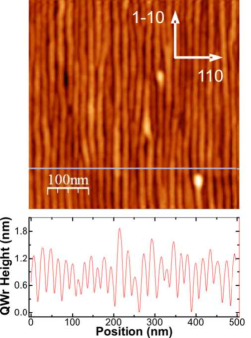
The InAs self-assembled QWRs were fabricated by solid source molecular beam epitaxy (MBE) on InP (001). More details about the QWR growth procedure can be found elsewhere. Fuster et al. (2005) For our present purpose, their most relevant physical properties are collected in Figure 1. The Atomic Force Microscopy (AFM) characterization of the uncapped sample reveals nm-thick self-assembled QWRs disposed along the (1-10) crystal direction and forming a continuous array across their perpendicular direction. The pitch period of the array (peak to peak) is nm and the average inter-QWr spacing at half-maximum is just nm. The uniformity of the array over large distances and the small separation are desirable characteristics for the fabrication of a QDh array and motivate this work.
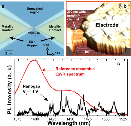
To fabricate the array, a sample was grown with the QWRs covered by 20 nm of InP and, next, two gate electrodes (10 nm Cr + 25 nm Au) were defined over the InP surface using electron beam lithography (EBL) and lift-off methods. The separation between the two electrodes along the (110) crystal direction was set to 200 nm meaning that 10 QWRs were embedded in the nanogap at this stage. The device geometry was delimited further defining etch stoppers in a second EBL step as shown in Figure 2(a). Both, the InP capping layer and the QWR layer were dry etched in the unmasked regions by reactive ion beam etching of InP using CH4:H2 buffered with N2. After the processing, the final layout of the device consists of a narrow rectangular channel (200300 nm) as shown in the AFM micrograph of Figure 2(b) where the QDh are allocated parallel to the electrode flat edges.
The PL spectrum of the nanodevice was analyzed using a fiber based confocal microscope working at 6 K. Continuous-wave excitation below the InP band gap was provided by a Ti-Sapphire laser ( nm) coupled to the excitation fiber. The micro-photoluminescence was collected with a different fiber and detected using a multichannel InGaAs photodiode array attached to a 0.5 m focal length spectrograph.
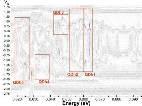
Figure 2(c) shows a PL spectrum obtained between the electrodes together with a reference ensemble PL spectrum recorded far away in a non-etched region. The latter is characteristic of the multimodal distribution of QWR heights observed by AFM. Alén et al. (2001) Meanwhile, the sharp spectral features recorded in the nanogap region must be associated to the emission of individual nanostructures allocated inside. Alén et al. (2006) In this situation, a lateral electric field can be applied to investigate the bias evolution of the observed resonances, as shown in Figure 3. Since the gate electrodes are arranged symmetrically on the surface, we observe that the dependence is approximately symmetrical with respect to V.
Generally, although the optical excitation generates matched electron-hole pairs, the electron and hole occupation in a given QDh is unequal and depends on the impurity background and on the different probabilities for electron and hole capture. Muñoz-Matutano et al. (2008) In our case, Hall resistance measurements reveal a n-type character ( cm-2) for the InP barriers favoring the formation of negatively charged excitons when no bias is applied. Alén et al. (2008) Also, carriers photogenerated at high energies must drift in the illuminated area and can be trapped in shallow traps associated to thickness fluctuations of the wetting layer before being captured in the QDh. Since the trapping efficiency is larger for holes, this mechanism can also lead to unbalanced charge configurations in the QDh. Moskalenko et al. (2006) In both situations, the number of confined carriers can be controlled applying a lateral electric field. The role of the bias is, for moderate values, to release the trapped charge which can now be collected in the QDh restoring the neutrality of the capture process Moskalenko et al. (2006) and, for larger positive or negative voltages, to bend the conduction and valence bands and enable the tunnelling of confined carriers out of the QDh. Alén et al. (2007)
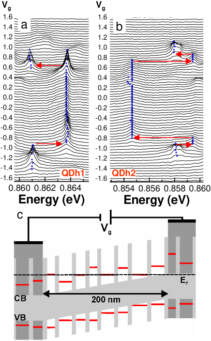
The behavior just described explains the bias evolution shown in Figure 4(a) where we have magnified a narrow region of the spectrum containing the emission of a single QDh (highlighted as QDh1 in Figure 3). A single resonance centered at 0.8636 eV characterizes the spectrum for V. In the midst of this range the intensity is smaller and increases towards both limits where it finds a maximum thanks to the enhanced carrier drift velocity. Moskalenko et al. (2006) Further positive or negative bias results indistinctly in a rapid quench of this resonance and the appearance of a new peak centered at 0.8608 eV. This happens after a change of the QDh net charge which shifts the ground state emission to lower energies due to the new balance between attractive and repulsive Coulomb terms. Alén et al. (2005) Given the abrupt character of the transition and the n-type character of the sample, the charging mechanism must be related to a tunnelling event occurring at this voltage as the fermi level crosses the conduction band levels. The positions of the energy jumps can be used thereafter to identify which resonances correspond to different QDh. Alén et al. (2005) If we keep increasing , as shown in Figure 3, all the emission lines finally disappear due to the fast tunnelling of carriers out of the QDh before they can recombine radiatively. Alén et al. (2007)
The general picture described for QDh1 is valid to explain the evolution of other QDhs in the array. For instance, Figure 4(b) shows the evolution of QDh2 which, in the same voltage range, suffers two charging events accompanied by two energy shifts of opposite sign. In our present device geometry, the charge state of the QDh depends mostly on the alignment of its confined levels with the chemical potential and therefore on the particular size and position of the QDh within the array [Fig. 4(c)]. Reimer et al. (2008b) Clearly, although the net electric charge can be varied in different QDh, its precise value can not be set in each one independently. This limitation, imposed by the size inhomogeneity inherent in self-assembled growth methods, could be solved in the future using individual gating technologies.
The average separation of 18 nm between QDh centers and the small nm edge to edge distance should be adequate to observe quantum tunnelling phenomena in this system. Krenner et al. (2005); Stinaff et al. (2006); Beirne et al. (2006) Yet, the mere observation of charging events does not imply a charge exchange between the QDh lined up between the electrodes. As stated above, the bias dependency of the carrier transport and tunnelling rates can explain our results as well. In the following, we will focus on the anomalous Stark shift found in different regions of the QDh array emission spectrum and discuss whether it can be interpreted in terms of indirect transitions among coupled QDh.
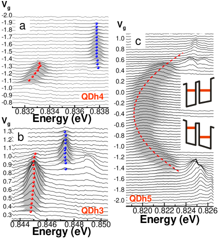
Figure 5(a) shows two resonances corresponding to QDh4 in its negative voltage range. Increasing the bias from V, the resonance at the left shifts to higher energies finding a maximum at V. The remarkable blue-shift cannot be explained from the quantum confined Stark effect of a direct exciton and distinguishes this resonance from those shown in figure 4(a) and (b). At V, the peak disappears and a new resonance becomes visible meV apart towards higher energies. The rest of Figure 5 depicts the dependence found for QDh3 in its positive bias range showing a similar pair of resonances split by meV [Fig. 5(b)], and the full evolution of QDh5 which demonstrates that the emission blue-shift is indeed symmetric around V [Fig. 5(c)].
Large energy splittings and anomalous Stark shifts, including blue-shifts similar to those shown in Figures 5(a) and (b), are spectral characteristics of vertically coupled QD molecules when an electron becomes delocalized between two QDs giving rise to resonance anticrossings. Krenner et al. (2005, 2006) For lateral molecules, however, the wavefunction overlap is smaller, quantum tunnelling splittings greater than a few hundred eV are unlikely, and anticrossings are hardly visible. Beirne et al. (2006) In addition, we observe the same evolution for opposite polarities of the bias [Fig. 3]. This is difficult to match within a resonant tunnelling scheme since two given electronic levels which are mutually aligned at , must be necessarily separated at , as shown schematically in Figure 5(c) for an asymmetric QDM. The possibility of two different anticrossings involving neutral and charged excitons as observed in vertical QDM, Stinaff et al. (2006); Krenner et al. (2006) can also be ruled out in our case where we find the same lines and splittings for both bias. We conclude that the anomalous Stark shift can not be related to an indirect transition. Recently, blue-shifting resonances have been observed in single InAs/InP QDs embedded between lateral electrodes. Reimer et al. (2008a) A theoretical model was able to explain them due to the field induced screening of the electron-hole interaction in a confined biexciton. Korkusinski et al. (2009) Alternately, the observed behavior could be related to a charging effect. As the device approaches the flat band condition at zero bias, more electrons populate the conduction band levels. In QWRs, such scenario of many electrons and few holes leads to the renormalization of the band gap energy and shifts the emission in the direction observed here. Akiyama et al. (2002) In QDs, highly charged exciton peaks also exhibit anomalous shifts in the flat band vicinity. Alén et al. (2005) Both interpretations, involving biexciton or highly charged exciton contributions, are consistent with the symmetric bias dependence. The latter also agrees with the n-type character of the InP barriers and the low excitation power used in our experiments.
Our results clearly show the limiting aspects of self-assembled growth methods for the fabrication of large arrays of coupled QDs. In our case, a possible spatial mismatch due to carrier localization along the QDh long axis has to be added to the electronic levels misalignment which often hampers the observation of quantum tunnelling phenomena. The recent development of pre-patterning methods where the position of QDs can be controlled without affecting their optical properties should encourage further work in this field. Reimer et al. (2008a); Martín-Sanchez et al. (2009)
In conclusion, we have fabricated an array of closely spaced quantum dashes by post-growth processing of a single layer of InAs/InP self-assembled quantum wires grown by solid source molecular beam epitaxy. The array was embedded in a lateral field effect structure which allowed the study of the emission spectrum of individual quantum dashes as a function of the applied bias. We have demonstrated that the net electric charge can be controlled and depleted in the individual nanostructures and that the energy position of their electronic levels can be modified. Our study reveals that size fluctuations prevent however an accurate control of these parameters necessary to fabricate large arrays of coupled QDs using this technology.
The authors acknowledge financial support by Spanish MEC and CAM through grants NANINPHO-QD (TEC2008-06756-C03-01/03), NANOCOMIC (S-505/ESP/000200) and Consolider-Ingenio 2010 QOIT (CSD2006-0019).
References
- Troiani et al. (2000) F. Troiani, U. Hohenester, and E. Molinari, Phys. Rev. B 62, R2263 (2000).
- Li et al. (2003) X. Li, Y. Wu, D. Steel, D. Gammon, T. H. Stievater, D. S. Katzer, D. Park, C. Piermarocchi, and L. J. Sham, Science 301, 809 (2003).
- Piermarocchi et al. (2002) C. Piermarocchi, P. Chen, L. J. Sham, and D. G. Steel, Phys. Rev. Lett. 89, 167402 (2002).
- Petta et al. (2005) J. R. Petta, A. C. Johnson, J. M. Taylor, E. A. Laird, A. Yacoby, M. D. Lukin, C. M. Marcus, M. P. Hanson, and A. C. Gossard, Science 309, 2180 (2005).
- Imamoglu et al. (1999) A. Imamoglu, D. D. Awschalom, G. Burkard, D. P. DiVincenzo, D. Loss, M. Sherwin, and A. Small, Phys. Rev. Lett. 83, 4204 (1999).
- Lovett et al. (2003) B. W. Lovett, J. H. Reina, A. Nazir, and G. A. D. Briggs, Phys. Rev. B 68, 205319 (2003).
- Hettich et al. (2002) C. Hettich, C. Schmitt, J. Zitzmann, S. . Kühn, I. Gerhardt, and V. Sandoghdar, Science 298, 385 (2002).
- Robledo et al. (2008) L. Robledo, J. Elzerman, G. Jundt, M. Atatüre, A. Högele, S. Fält, and A. Imamoglu, Science 320, 772 (2008).
- Kim et al. (2008) D. Kim, S. E. Economou, S. C. Badescu, M. Scheibner, A. S. Bracker, M. Bashkansky, T. L. Reinecke, and D. Gammon, Phys. Rev. Lett. 101, 236804 (2008).
- Stinaff et al. (2006) E. A. Stinaff, M. Scheibner, A. S. Bracker, I. V. Ponomarev, V. L. Korenev, M. E. Ware, M. F. Doty, T. L. Reinecke, and D. Gammon, Science 311, 636 (2006).
- Krenner et al. (2005) H. J. Krenner, M. Sabathil, E. C. Clark, A. Kress, D. Schuh, M. Bichler, G. Arbsreiter, and J. J. Finley, Phys. Rev. Lett. 94, 057402 (2005).
- Beirne et al. (2006) G. J. Beirne, C. Hermannstädter, L. Wang, A. Rastelli, O. G. Schmidt, and P. Michler, Phys. Rev. Lett. 96, 137401 (2006).
- Lee et al. (2001) H. Lee, J. A. Johnson, M. Y. He, J. S. Speck, and P. M. Petroff, Appl. Phys. Lett. 78, 105 (2001).
- Alonso-González et al. (2007) P. Alonso-González, L. González, Y. González, D. Fuster, I. Fernández-Martínez, J. Martín-Sánchez, and L. Abelmann, Nanotechnology 18, 355302 (2007).
- Sun et al. (2002) K. W. Sun, J. C. Wu, B. C. Lee, and C. P. Lee, Nanotechnology 13, 576 (2002).
- Lefebvre et al. (2002) J. Lefebvre, P. J. Poole, J. Fraser, G. C. Aers, D. Chithrani, and R. L. Williams, J. Cryst. Growth 234, 391 (2002).
- Sugaya et al. (2007) T. Sugaya, I. Morohashi, K. Komori, and T. Amano, J. Cryst. Growth 301, 762 (2007).
- Mano et al. (2002) T. Mano, R. Nötzel, G. J. Hamhuis, T. J. Eijkemans, and J. H. Wolter, Appl. Phys. Lett. 81, 1705 (2002).
- Mazur et al. (2003) Y. I. Mazur, W. Q. Ma, X. Wang, Z. M. Wang, G. J. Salamo, M. Xiao, T. D. Mishima, and M. B. Johnson, Appl. Phys. Lett. 83, 987 (2003).
- Leon et al. (2002) R. Leon, S. Chaparro, S. R. Johnson, C. Navarro, X. Jin, Y. H. Zhang, J. Siegert, S. Marcinkevicius, X. Z. Liao, and J. Zou, J. Appl. Phys. 91, 5826 (2002).
- Welsch et al. (2008) H. Welsch, T. Kipp, T. Köppen, C. Heyn, and W. Hansen, Semicond. Sci. Technol. 23, 045016 (2008).
- Bauer et al. (2004) J. Bauer, D. Schuh, E. Uccelli, R. Schulz, A. Kress, F. Hofbauer, J. J. Finley, and G. Abstreiter, Appl. Phys. Lett. 85, 4750 (2004).
- Reimer et al. (2008a) M. E. Reimer, M. Korkusinski, D. Dalacu, J. Lefebvre, J. Lapointe, P. J. Poole, G. C. Aers, W. R. McKinnon, P. Hawrylak, and R. L. Williams, Phys. Rev. B 78, 195301 (2008a).
- Fuster et al. (2005) D. Fuster, L. González, Y. González, M. U. González, and J. Martínez-Pastor, J. Appl. Phys. 98, 033502 (2005).
- Alén et al. (2001) B. Alén, J. Martínez-Pastor, A. García-Cristóbal, L. González, and J. M. García, Appl. Phys. Lett. 78, 4025 (2001).
- Alén et al. (2006) B. Alén, D. Fuster, Y. González, L. González, and J. Martínez-Pastor, Appl. Phys. Lett. 89, 233126 (2006).
- Muñoz-Matutano et al. (2008) G. Muñoz-Matutano, B. Alén, J. Martínez-Seravalli, P. Frigeri, and S. Franchi, Nanotechnology 19, 145711 (2008).
- Alén et al. (2008) B. Alén, D. Fuster, G. Muñoz-Matutano, J. Martínez-Pastor, Y. González, J. Canet-Ferrer, and L. González, Phys. Rev. Lett. 101, 067405 (2008).
- Moskalenko et al. (2006) E. S. Moskalenko, M. Larsson, W. V. Schoenfeld, P. M. Petroff, and P. O. Holtz, Phys. Rev. B 73, 155336 (2006).
- Alén et al. (2007) B. Alén, J. Bosch, J. Martínez-Pastor, D. Granados, J. M. García, and L. González, Phys. Rev. B 75, 045319 (2007).
- Alén et al. (2005) B. Alén, J. Martínez-Pastor, D. Granados, and J. M. García, Phys. Rev. B 72, 155331 (2005).
- Reimer et al. (2008b) M. E. Reimer, W. R. McKinnon, J. Lapointe, D. Dalacu, P. Poole, G. C. Aers, D. Kim, M. Korkusinski, P. Hawrylak, and R. L. Williams, Physica E 40, 1790 (2008b).
- Krenner et al. (2006) H. J. Krenner, E. C. Clark, T. Nakaoka, M. Bichler, C. Scheurer, G. Abstreiter, and J. J. Finley, Phys. Rev. Lett. 97, 076403 (2006).
- Korkusinski et al. (2009) M. Korkusinski, M. E. Reimer, R. L. Williams, and P. Hawrylak, Phys. Rev. B 79, 035309 (2009).
- Akiyama et al. (2002) H. Akiyama, L. N. Pfeiffer, A. Pinczuk, K. W. West, and Y. Masahiro, Solid State Comm. 122, 169 (2002).
- Martín-Sanchez et al. (2009) J. Martín-Sanchez, G. Muñoz-Matutano, J. Herranz, J. Canet-Ferrer, B. Alén, Y. González, P. Alonso-González, D. Fuster, L. González, J. Martínez-Pastor, et al., ACS Nano 3, 1513 (2009).
List of figures
Figure 1.- Top panel: 500500 nm AFM image of an uncapped sample showing the initial QWR planar array. Bottom panel: Profile along the (110) crystal direction of the same AFM image.
Figure 2.- (a) Optical image of the device before the dry etching step. (b) AFM micrograph of the fully processed 200 nm wide nanogap containing the array of InAs/InP QDh. (c) Ensemble PL of the unprocessed sample and PL spectrum in the nanogap obtained at 6 K.
Figure 3.- Full evolution of the PL spectrum recorded in the nanogap region with external bias. Highlighted regions enclose the emission of individual QDhs as discussed in the text.
Figure 4.- a) and b) Different spectral regions where the coulomb blockade effects dominate the bias evolution of the PL spectrum. The horizontal arrows indicate the voltages where the net electric charge changes in each QDh. c) Schematics of the device band structure along the 110 crystal direction in the QDh array region.
Figure 5.- a), b) and c) Different spectral regions where individual resonances experience a blue-shift with increasing bias (solid dots in a) and b) indicate the positions of the maxima performing gaussian fits, dashed line in c) is a guide to the eye). The evolution is symmetric around V as observed in panel c) and Fig. 3.
