Inhomogeneous vortex-state-driven enhancement of superconductivity in nanoengineered ferromagnet-superconductor heterostructures.
Abstract
Thin film heterostructures provide a powerful means to study the antagonism between superconductivity (SC) and ferromagnetism (FM). One interesting issue in FM-SC hybrids which defies the notion of antagonistic orders is the observation of magnetic field induced superconductivity (FIS). Here we show that in systems where the FM domains/islands produce spatial inhomogeneities of the SC order parameter, the FIS can derive significant contribution from different mobilities of the magnetic flux identified by two distinct critical states in the inhomogeneous superconductor. Our experiments on nanoengineered bilayers of ferromagnetic CoPt and superconducting NbN where CoPt/NbN islands are separated by a granular NbN, lend support to this alternative explanation of FIS in certain class of FM-SC hybrids.
The pinning of magnetic flux lines in a superconducting (SC) film by ferromagnetic (FM) dots and multidomain magnetic films has been a topic of considerable interest Lyuksyutov ; Lange1 ; Igor ; Buzdin ; Gillijns ; Pissas ; Morgan1 ; Bekaert . An important consequence of the inhomogeneous magnetic field produced by such structures is the formation of a local field-free state when the FM-SC hybrid is placed in an external magnetic field. This effect has been variously called as field-enhanced superconductivity Lyuksyutov ; Lange1 , magnetization controlled superconductivity Igor and domain wall superconductivity Buzdin ; Gillijns .
Earlier studies of FM-SC hybrids have been carried out mostly on films of elemental superconductor such as Nb and Pb deposited on in-plane as well as high coercivity perpendicular anisotropy media Lyuksyutov ; Lange1 ; Igor ; Buzdin ; Gillijns ; Pissas ; Morgan1 ; Bekaert . Although striking field-induced changes in the critical temperature (Tc) of the superconductor have been seen, the field-free regions produced by the dipolar field of FM dots are not homogeneous in these systems. Also, it is not clear whether superconductivity actually survives in areas above (or below) the dots because of the small upper critical field (Hc2) of the elemental superconductors and strong magnetization of the dots. The global superconducting order parameter in these FM-SC hybrids is clearly inhomogeneous irrespective of the orientation of magnetization in the dots. It is therefore, important to address the possible role of granularity in causing the FIS in such systems. The relevance of this issue becomes apparent from the richness of the field-temperature (H-T) phase diagram of well-known granular systems such as composite films Vinokur , high Tc ceramics Tinkham and Josephson-junction arrays Martinoli .
In this report we address field-induced superconductivity in nanoengineered grids of CoPt/NbN where the CoPt-free regions have been made granular, with a reduced Tc. The advantage of using NbN is in its large Hc2 ( 250 kOe) which prohibits a significant perturbation of superconductivity by the CoPt. The resistance (R) of the nanoengineered structures has been measured with current density J Jc as a function of external field applied in two different orientations; (i) ( ) , and (ii), ( ) , where is a unit vector normal to the plane of the film. The R vs. H loops are hysteretic with their reverse branch showing entry into the superconducting state at fields much higher than the field at which R appears in the forward branch. This FIS state is shown to be a consequence of the granularity of magnetic and superconducting order parameters in the hybrid.
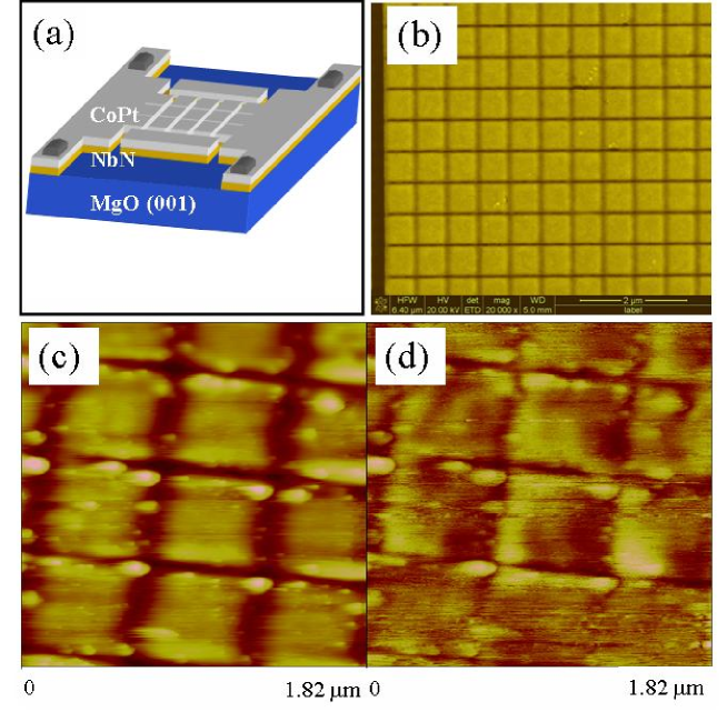
Thin film bilayers of CoPt and NbN each 50 nm thick, were deposited on (001) MgO at 600 0C using pulsed laser ablation of CoPt and Nb targets respectively. Further details of the deposition of NbN and CoPt films are given elsewhere Rakshit ; Senapati ; Budhani . The bilayer film was first patterned with standard lithography and then Ar+ ion milled into a 100 m500 m bridge as shown in Fig. 1. The top CoPt layer was then structured in simple square patterns using a Ga3+ focused ion beam (FIB) milling facility. Fig. 1(b) shows a typical scanning electron micrograph of the patterned bilayer. The size of each CoPt element in the pattern is 0.50.5 m2 with 50 nm spacing in between. The active area of the sample on which transport measurements were carried out contains 10210 square elements.
The magnetic domain structure of the CoPt squares was probed with Magnetic Force Microscopy (MFM) and Atomic Force Microscopy (AFM) performed simultaneously on a thermally demagnetized sample in the tapping mode at various lift heights. A commercial magnetometer was used for measurement of magnetization. The critical current density (Jc), resistance R (T) and magnetoresistance R (H) were measured between 5 and 20 K.
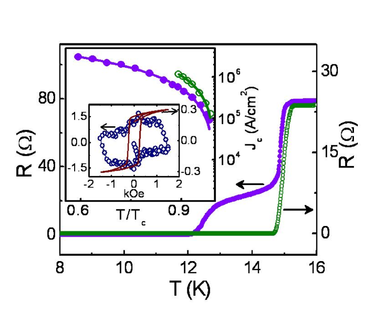
Since the central result of this paper is based on inhomogeneities of the SC and FM order parameters, we first establish these inhomogeneities in the patterned sample. Fig. 2 presents R (T) of the patterned as well as unpatterned bilayer. While the latter film shows a sharp transition (T 0.5 K) with Tc onset at 15.3 K, the R (T) of the patterned film exhibits a two step structure - where the first drop in resistance occurs at 15.1 K in which R decreases by 60 of its normal state value. The second transition starts at 13 K, culminating in R = 0 at 11.8 K. The change from single-step to two-step transition on nanostructuring is presumably a result of Ga3+ ion damage. This feature, however, provides the unique advantage of addressing FIS in a granular medium. Inset of Fig. 2 compares the Jc (T) of the nanostructured and a plane bilayer film. The Jc of the unpatterned film quickly reaches the limit of our measurement which is set by the width of the bridge and maximum current used ( 100 mA). However, a pronounced reduction in the Jc is seen on nanopatterning. Since the capacity of such structures to carry dissipation-less current is determined by their low Tc links, a suppressed growth of Jc on lowering the temperature indicates that the channels of NbN connecting CoPt/NbN islands are granular.
Fig. 2 also shows magnetization (M) of an unpatterned bilayer at 5 and 20 K as a function of magnetic field applied along the surface of the film. The square hysteresis loop of low coercivity ( 250 Oe) at 20 K seen here suggests a soft ferromagnetic state in CoPt with in-plane , a characteristic feature of the disordered fcc phase of CoPt Budhani . The M-H curve traced at 5 K is dominated by the diamagnetic response of the NbN layer. While it was not possible to measure the magnetic state of the patterned film with SQUID magnetometry, we have used room temperature MFM to visualize domain structure of the CoPt islands. Fig. 1(c) and (d) show the AFM and MFM micrographs respectively, taken from the same spot on the film Text . The bright and dark features in MFM represent domains of reversed . Since each patterned CoPt island has two such domains, it is clear that they are in a thermally demagnetized state.
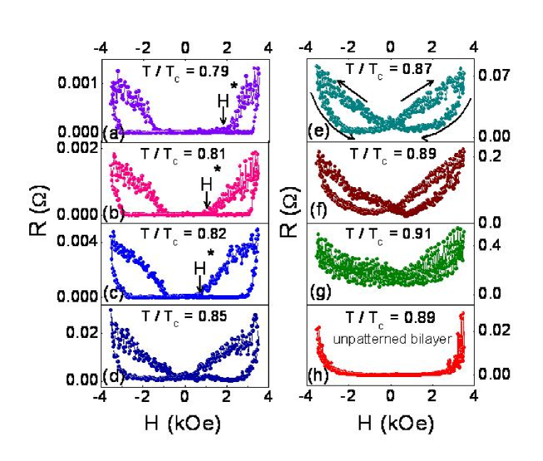
In Fig. 3, we show a set of R (H) data for the nanostructured film at several T/Tc, where Tc is the temperature ( 11.8 K) at which zero-resistance state is reached. The magnetic field applied in the plane of the film and orthogonal to current in these measurements, was scanned in units of kOe following the cycle 0 3.5 0 - 3.5 0. A constant current density of 1106 A/cm2, which corresponds to the Jc at 9.8 K (T/Tc = 0.83) was used for resistance measurements. At small T/Tc (= 0.79), the R first remains zero with the increasing field. This is expected as the zero-field current density J is smaller than the Jc at this T/Tc. However, as the field increases, Jc drops and at H = H∗ (marked in the figure), the J becomes larger than Jc and the sample goes in a dissipative state. Here the dependence of R is linear on H, as expected in the flux flow regime of the mixed state. On reversing the field, however, the resistance drops to zero much faster. The dissipation-less state appears at a higher field H ( H∗) in the reverse branch of the loop. A similar hysteretic behavior is seen at the higher values of T/Tc. In Fig. 3 (h) we show the result of a similar measurement performed on an unpatterned bilayer. In this case the R vs. H curve is completely reversible. It is clear from these measurements that the hysteretic behavior of R vs. H is a consequence of the nano-patterning. This is the central result of our paper.
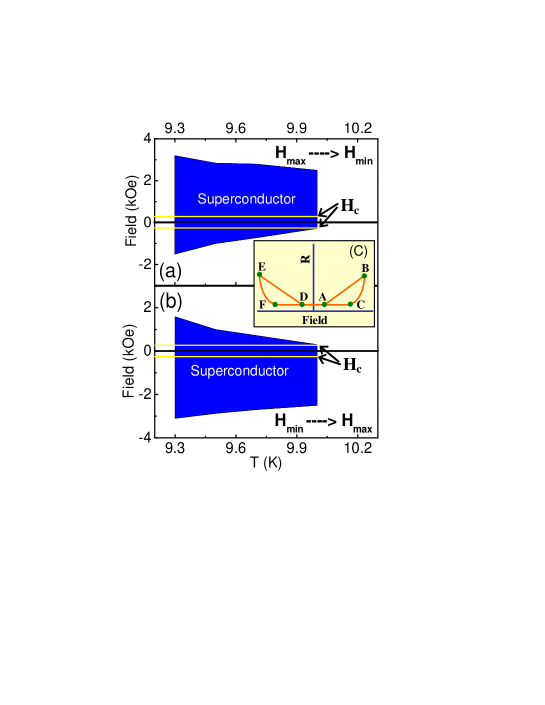
In Fig. 4(a) and (b) we summarize these observations of a field-assisted reentrant superconducting state in terms of H-T phase diagram. Fig. 4(c) shows a sketch of the R-H curve whose critical points have been marked by letters A, B, C, D, E and F. The point A corresponds to H∗ where superconductivity disappears on ramping up the field, point B denotes the maximum applied field and point C is where superconductivity reappears on reducing the field from its maximum value. Similarly, points D and F mark destruction and reappearance of SC on the reverse branch of the loop while E corresponds to the maximum negative field. The contours of the points C and D as a function of temperature are shown in Fig. 4(a), and the shaded area enclosed by them is the range of field where global superconductivity exists while scanning it from + Hmax to - Hmax. Fig. 4(b) is the phase space of superconductivity for - Hmax to + Hmax excursion.
Before attempting to put forward a model which would allow us to understand the results of Fig. 3 and 4, it is important to point out that for our film of thickness d ( 50 nm) much smaller than the penetration depth ( 200 - 250 nm) placed in a parallel field, a large contribution to dissipation may come from orbital and Pauli pair-breaking processes, in addition to the dissipation due to flux flow. However, the pair breaking processes are not hysteretic. The misalignment of the magnetic field away from a true parallel configuration is also an important issue because the parasitic out-of-plane component of the field can lead to nucleation of perpendicular vortices. To rule out this possibility, we had aligned the field parallel to the plane of the film with a precision of 0.1 degree using a specially built experimental setup Patnaik .
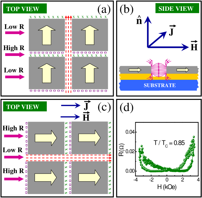
A correct model for understanding the phase diagram of Fig. 4 must take into account two important features of the nano-structured sample; first, it has a periodic granularity. The CoPt-NbN squares become superconducting at 15.1 K, but a long-range phase coherence develops only when the CoPt-free grids go superconducting at 11.8 K. The patterned film therefore is characterized by two distinct critical current densities, a large Jcg inside the NbN-CoPt squares and a much weaker Jcj in the channels separating these squares. Secondly, the CoPt islands have in-plane with coercive field 250 Oe (see Fig. 2) which has been marked by a pair of horizontal lines in the phase diagram of Fig. 4. It is clear that in most of the phase space, the CoPt islands are saturated with their . A qualitative understanding of the flux distribution can be made from Fig. 5(a) and (c) drawn for ( ) and ( ) configurations. We show that even when CoPt squares are flux coupled at H Hc, some fringing field from the edges of the squares produces flux lines of opposite polarity in the NbN channels. These are marked by open circles and crosses in the top view of the square array. The flux due to external magnetic field has a different distribution in the channels and the CoPt covered NbN squares because of their different Jc’s. It can be understood in the framework of the two-level critical state model of Ji, Rzchowski, Anand, and Tinkham Ji . Using this model we can define two types of fluxons; (i) those pinned by pinning centers in the square (p), and (ii), the fluxons that are confined to the channels and are free to move due to weak pinning (f). As the external field is increased, fluxons enter the channels first, supersaturating them and leading to the increase of dissipation along A-B branch of the curve in Fig. 4(c). The flux eventually enters the squares where it is pinned. On decreasing the field, the free flux (f) leaks out from the channels to such an extent that the zero resistance state is reestablished along the low resistance paths marked in Fig. 5 at a higher value of the external field. This is possible because there is a large pinned flux (p) in the NbN squares.
We expect that in the configuration (Fig. 5(a)), the current flow along the channels (paths which do not cross CoPt-NbN squares) remain dissipative due to the dipolar field of CoPt. This is where the magnetization of CoPt plays an explicit role. A similar scenario also explains reentrant superconductivity seen for the configuration sketched at the left bottom panel (c) of Fig. 5. A typical set of R vs. H data taken at T/Tc = 0.85 in configuration is shown in panel (d) of Fig. 5. The granular NbN channels although form a continuous path for the flow of current for , the cores of vortices, which are already large due to a small order parameter in the channels, start overlapping, and even at low fields, the channels become resistive. The onset of resistance here has nothing to do with vortex motion under Lorentz force. This type of force-free dissipation has been seen in granular films of NbN Dhkim .
The observations made in the present study have important repercussions on the phenomenon of field assisted superconductivity seen in FM-SC bilayers Yu , trilayers Gu and dot structures Lange1 . While in the case of FM-SC-FM trilayer structures placed in an in-plane field, no inhomogeneity of the order parameter is introduced as long as each FM layer behaves like a single domain film, the same is unavoidable in bilayers at field H Hc and in dot arrays even beyond saturation. We believe that in such systems the repercussions of the two-level critical state model warrant consideration.
This research has been supported by a grant from the Nanoscience Nanotechnology Initiative of the Department of Science Technology, Government of India, and internal funding of IIT Kanpur. We thank Professor G. K. Mehta for his support in setting up the FIB facility and to S. K. Bose, R. Sharma, and S. Srivastava for technical assistance.
REFERENCES:
References
- (1) I. F. Lyuksyutov and V. L. Pokrovsky, Adv. Phys. 54, 67 (2005).
- (2) M. Lange, M. J. Van Bael, Y. Bruynseraede, and V. V. Moshchalkov, Phys. Rev. Lett. 90, 197006 (2003).
- (3) I. F. Lyuksyutov and V. Pokrovsky, Phys. Rev. Lett. 81, 2344(1998).
- (4) A. Yu. Aladyshkin, A. I. Buzdin, A. A. Fraerman, A. S. Mel’nikov, D. A. Ryzhov, and A. V. Sokolov, Phys. Rev. B 68, 184508 (2003).
- (5) W. Gillijns, A. Y. Aladyshkin, M. Lange, M. J. Van Bael, and V. V. Moshchalkov, Phys. Rev. Lett. 95, 227003 (2005).
- (6) D. Stamopoulos, M. Pissas, V. Karanasos, and D. Niarchos, Phys. Rev. B 70, 054512 (2004).
- (7) D. J. Morgan, and J. B. Ketterson, Phys. Rev. Lett. 80, 3614 (1998).
- (8) M. J. Van Bael et al., Phys. Rev. Lett. 86, 155 (2001).
- (9) I. S. Beloborodov, A. V. Lopatin, V. M. Vinokur, and K. B. Efetov, Rev. Mod. Phys. 79, 469 (2007).
- (10) M. Tinkham and C. J. Lobb, in Solid State Physics, edited by H. Ehrenreich and D. Turnbull 42, 91 (Academic Press, San Diego, 1989).
- (11) P. Martinoli and C. T. Leemann, Low Temp. Phys. 118 699 (2000).
- (12) R. K. Rakshit, S. K. Bose, R. Sharma, and R. C. Budhani, Appl. Phys. Lett. 89, 202511 (2006).
- (13) R. K. Rakshit, S. K. Bose, R. Sharma, R. C. Budhani, T. Vijaykumar, S. J. Neena, and G. U. Kulkarni, J. Appl. Phys. 103, 023915 (2008).
- (14) K. Senapati, N. K. Pandey, R. Nagar, and R. C. Budhani, Phys. Rev. B 74, 104514 (2006).
- (15) Simultaneous sampling of magnetic and topographic images at different lift heights (even upto 120 nm) ruled out any topographical artifact presents in MFM image.
- (16) S. Patnaik, K. Singh, and R. C. Budhani, Rev. Sci. Instrum. 70, 1494 (1999).
- (17) L. Ji, M. S. Rzchowski, N. Anand, and M. Tinkham, Phys. Rev. B 47, 470 (1993).
- (18) D. H. Kim, K. E. Gray, R. T. Kampwirth, K. C. Woo, D. M. McKay, and J. Stein, Phys. Rev. B 41, 11642 (1990).
- (19) A. Y. Rusanov, M. Hesselberth, J. Aarts, and A. I. Buzdin, Phys. Rev. Lett. 93, 057002 (2004).
- (20) J. Y. Gu, C.-Y. You, J. S. Jiang, J. Pearson, Y. B. Bazaliy, and S. D. Bader, Phys. Rev. Lett. 89, 267001 (2002).
FIGURE CAPTIONS:
Fig. 1. A schematic of the sample design is shown in panel (a). Panel (b) shows a scanning electron micrograph of the patterned bilayer, and panels (c) and (d) AFM and MFM images respectively. AFM and MFM measurements were performed simultaneously on thermally demagnetized samples at lift height of 40 nm. AFM image of the sample is quite similar to its SEM image. The bright and dark features in MFM represent domains of reversed magnetization.
Fig. 2. R (T) of the patterned (filled circles) and unpatterned (open circles) bilayers. A clear two-step superconducting transition is seen in the patterned film. Inset shows Jc of the unpatterned (open circles) and patterned (solid circles) samples. M vs. H loops for an unpatterned bilayer sample at 5 K (open symbols) and 20 K (solid line) with field applied parallel to the film surface are also shown in the inset. Here the magnetization is measured in units of 10-3 emu.
Fig. 3. R (H) of the nanoengineered CoPt-NbN/MgO bilayer is shown in panel (a) to (g) at several T/Tc. Small arrows in panel (e) mark the direction of field sweep. The critical field H∗ at which dissipation appears on ramping the field from zero has also been marked in the figures with vertical arrows. Panel (h) shows R (H) of the unpatterned sample at T/Tc = 0.89.
Fig. 4. The dark areas in panel (a) and (b) show the H-T phase space where the FIS exists as shown by results of Fig. 3. Panel (c) sketches the R-H curve in which critical points have been marked by letters A, B, C, D, E and F. The contours of the points C and D as a function of temperature are shown in (a) while scanning the field from + Hmax to - Hmax. Contours of points F and A are shown in panel (b) for the field scan from - Hmax to + Hmax. The coercive field Hc = 250 Oe is drawn by a pair of horizontal lines in both the phase diagrams.
Fig. 5. Panel (a) Top view of flux distribution for ( ). In-plane field lines are shown as dotted lines whereas the dipolar field penetrating the NbN channel is shown by circles and crosses. Large arrows in the middle of squares mark the direction of of CoPt islands. A side view of the dipolar field produced by the CoPt is sketched in panel (b). Panel (c) shows the flux distribution when and are collinear. Panel (d) shows R vs. H plot in configuration at T/Tc = 0.85.
