Direct observation of a Fermi surface and superconducting gap in LuNi2B2C
Abstract
We measured the Fermi surface (FS), band dispersion and superconducting gap in LuNi2B2C using Angle Resolved Photoemission Spectroscopy. Experimental data were compared with the tight-binding version of the Linear Muffin-Tin Orbital (LMTO) method and Linearized Augmented Plane-Wave (LAPW) calculations. We found reasonable agreement between the two calculations and experimental data. The measured FS exhibits large parallel regions with a nesting vector that agrees with a previous positron annihilation study and calculations of the generalized susceptibility. The measured dispersion curves also agree reasonably well with the TB-LMTO calculations, albeit with some differences in the strength of the hybridization. In addition, the spectrum in the superconducting state revealed a 2meV superconducting gap. The data also clearly shows the presence of a coherent peak above the chemical potential, that originates from thermally excited electrons above the energy of 2. This feature was not previously observed in the Lu-based material.
pacs:
74.70.Dd, 71.18.+y, 71.20.-b, 71.27.+aI Introduction

Rare earth nickel borocarbides RNi2B2C (R - rare earth) constitute an interesting class of materials Cava1994 ; Nagarajan1994 ; Canfield1998 ; MullerNarozhnyi2001 ; MazumdarNagarajan2005 , in which there is a competition and coexistence between superconductivity and magnetism. Amongst these compounds, nonmagnetic LuNi2B2C has the highest superconducting critical temperature of 16.6 K Cava1994 . The borocarbides exhibit a peculiar anisotropy of the superconducting gap, the character of which is still under debate. It is believed that the gap is highly anisotropic in the two non-magnetic compounds LuNi2B2C and YNi2B2C Boaknin2001 ; Bobrov2005 ; Maki2002 ; Raychaudhuri2004 ; MartinezSamper2003 ; Izawa2002 ; Yokoya2000 . Its symmetry was proposed to be s + g Maki2002 , which is consistent with certain experimental results Raychaudhuri2004 but an anisotropic s-wave symmetry has also been considered MartinezSamper2003 . Other experimental data indicate that the gap in YNi2B2C has point nodes along the (100) and (010) directions Izawa2002 . LuNi2B2C crystallizes in a body-centered tetragonal structure with lattice parameters a = 3.4639 Å, and c = 10.6313 ÅSiegrist1994 . Its crystal structure consists of Lu-C layers with Ni2B2 sheets in between. Previously calculations reveal that LuNi2B2C is characterised by a large density of states (DOS) at the Fermi energy () originating mainly, but not exclusively, from Ni d electrons Mattheiss1994 ; PickettSingh1994 ; Coehoorn1994 . Another interesting feature is a flat band along the -X direction just above . The Fermi surface (FS) topography of LuNi2B2C was studied by ab-initio calculations Rhee1995 ; Kim1995 ; Dugdale1999 . Band structure calculations Rhee1995 revealed a pronounced maximum in the generalized electronic susceptibility at (0.6a*, 0, 0), where a* and most likely arising from large nested regions of the FS. Moreover, phonon softening was observed in LuNi2B2C by means of inelastic neutron scattering for a range of wave vectors around (0.5a*, 0, 0) Dervenagas1995 . Interestingly enough the magnetic ordering, which was found in RNi2B2C compounds with magnetic atoms R = Er, Ho, Tb and Gd manifest similar modulation vector usually close to (0.55a*,0,0)MullerNarozhnyi2001 . The first experimental studies of the LuNi2B2C (RNi2B2C) Fermi surface were performed by means of two-dimensional angular correlation of electron-positron annihilation radiation (2D-ACAR) and the data were compared to the Linear Muffin-Tin Orbital (LMTO), local density approximation (LDA) calculations Dugdale1999 . Nested parts of the FS were found with a nesting vector corresponding to both the phonon softening and the magnetic modulation vectors. The fraction of the FS participating in nesting was determined to be 4.4 0.5% Dugdale1999 . That study was however limited only to a rough “calipering” of the Fermi surface. Knowledge of the experimental band structure, Fermi surface and quasiparticle properties is deemed essential to understand the interplay of the various interactions in these materials, as it may shed new light on other phenomena such as anisotropic superconductivity, the role of phonon softening and the relationship between the superconductivity and magnetic ordering in the borocarbides. It is also a pre-requisit for direct determination of the alleged anisotropy of the superconducting gap in these materials. In this report we present angle resolved photoelectron spectroscopy (ARPES) measurements of the band dispersion, Fermi surface and supercondcuting gap in the borocarbide with the highest , LuNi2B2C. The experimental results were compared with the tight-bounding LMTO (TB-LMTO) method and the full potential LAPW calculations. We found reasonable agreement with theory. The most significant difference between the calculations and experimental data is the strength of the hybridization. We also determined the superconducting gap to be 2.58 meV (extrapolated for T=0), in good agreement with the gap expected from the superconducting transition temperature ().
II Experimental
LuNi2B2C single crystals were grown at Ames Laboratory by means of a high-temperature flux techniqueCanfield1998 ; Fisher2001 . The plate-like crystals were cleaved in situ at pressures better than 3 x 10-11 Tr to reveal and maintain fresh a-b surfaces. The Fermi surface and band structure mapping were performed at the 7.0.1 beamline at the Advanced Light Source, using a Scienta R4000 analyzer. The energy and angle resolution were set at 30 meV and 0.5 deg, respectively. The energy gap was measured with a Scienta 2002 analyser and He-I photon source (h = 21.2 eV), in which the overall energy resolution was set at 2 meV. The normal state data were measured at the Synchrotron Radiation Center using the PGM beamline and Scienta 2002 endstation, with the energy and angular resolution set at 13 meV and 0.25 deg, respectively. Tight-binding linear muffin-tin orbital calculations were performed by the TB-LMTO program, version 47 LMTO , and the Full-Potential Linearized Augmented Plane-Wave (LAPW) calculations were performed using the Wien2k package Wien .

III Results and discussion
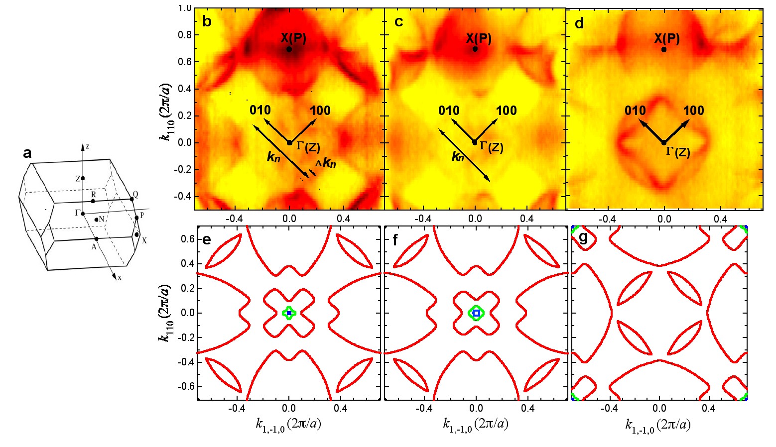
Band structure and semi-planar Fermi Surface cuts were determined for incident photon energies 128.13 eV, 119.44 eV and 102.98 eV (Fig. 1b-d), where the point in the Brillouin zone (Fig. 1a) corresponds to normal emission of electrons along the (001) direction. A correction term ( is the distance from the point) was used to account for mapping of the momentum space onto the angular distribution of photoelectrons. The ARPES process in 3D materials leaves some ambiguity as to the component of the momentum (perpendicular to the sample surface), because it is not conserved in the photoemission process. This is due to jump of the potential at the sample surface. From conservation of energy and remaining components of the momentum one can calculate the relative changes of the for various photon energies. To obtain the offset one needs to seek guidance from the band structure calculations and identify the high symmetry points in the data.HUFNER This allows estimation of the offset. The change of the wave vector component (parallel to the c axis) between scans in Fig. 1b (=128.13) and 1c (=119.44) was calculated from momentum and energy conservation to be 0.33 of the -Z distance. Similarly the change of the wave vector component between scans in Fig. 1c (=119.44) and 1d (=102.98) was 0.66 of the -Z. The calculated Fermi surfaces were obtained for constant values by means of the TB-LMTO method and are shown in Fig. 1 panels e-g. We estimated the values of the inner potential, = 9.4 eV and the work function = 4.6 eV, by comparing the high symmetry points between the calculated Fermi surfaces and the experimental data. This allowed us to determine the offset of the photon energy that corresponds to = 0.
The Fermi surface maps for the incident photon energies of 128.13 eV and 119.44 eV reveal large parallel parts of the FS with essentially the same nesting vector (spacing between the linear sections): = (0.59 0.04)a* for Fig. 1b and = (0.58 0.04)a* for Fig. 1c. is expressed in the units of the -Z distance, where the point corresponds to = 0. Although the full three dimensional FS was not determined in great detail, a similar nesting vector was found for different values which indicates that the FS likely has considerable nesting properties for a wide range of values. The constancy of the value of the nesting vector between =0.15 and -0.2 is also consistent with results of calculations. The spacing between the parallel segments of the Fermi surface predicted by TB-LMTO calculation is between 0.54a* and 0.55a*, the LAPW calculation results (not shown) are 0.50a* and 0.57a*, respectively. The detected is very close to the theoretically predicted value obtained from the generalized susceptibility Rhee1995 . Our results also agree reasonably well with the nesting vector previously determined via 2D-ACAR Dugdale1999 .
The Fermi surface map obtained at 102.98 eV very closely resembles the calculated Fermi surface for = 0.8a*. The overall shapes of the measured and calculated Fermi surface sheets (Fig. 1d and 1g) are very similar, however there is one significant difference. In the calculations the four oval parts of the Fermi surface centered about -Z are well separated in momentum space (Fig. 1g), while the data reveals that they actually are connected at the edges (Fig. 1d). A lack of separation in the experimental data may indicate that the hybridization gap is overestimated in the calculations. These oval parts arise from the intersection of the electron and hole-like bands. Interestingly enough at the edges along the diagonal directions (e. g. 110) the bottom of the electron band and the top of the hole band appear to be pinned at the chemical potential, resulting in a characteristic “flower” shape.
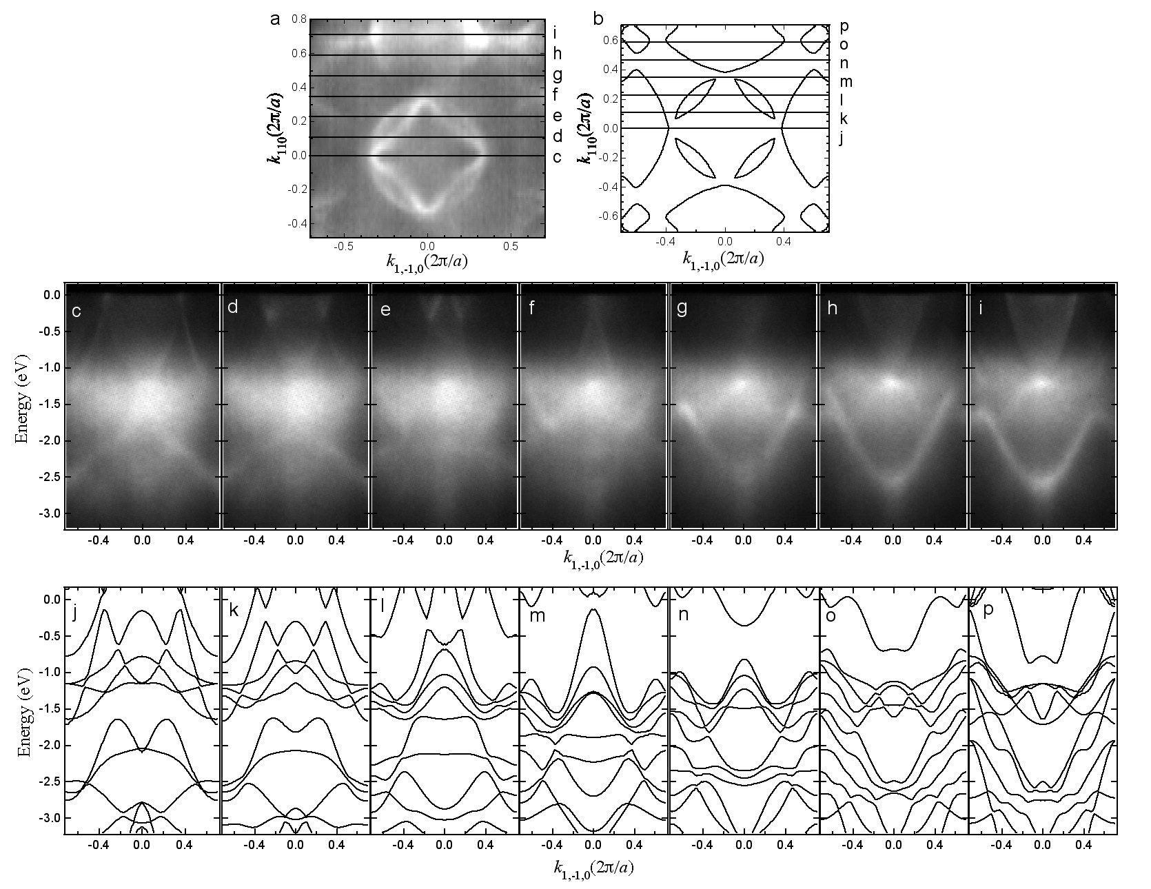
In Fig. 2 we plot the band dispersion data along a few selected cuts in momentum space obtained at an incident photon energy of 102.98 eV (Figs. 2c-i), along with a calculated (TB-LMTO method) band dispersion for 0.8a* (Figs. 2j-p). The agreement between the measured and calculated band dispersion is rather good, especially in the proximity of the chemical potential. In the corresponding TB-LMTO calculations (Figs. 2j-p), the same overall features are well reproduced, which shows the validity of the calculation in this material to a certain extent. This agreement also validates the assignment of values to the cuts measured at various photon energies, which is very important when studying 3D materials with ARPES. The most significant difference is the hybridization gap, which is quite large in the calculations but its signatures are for the most part absent in the measured data. For example in Fig. 2 panels (k) and (l) the high and low energy branches form hybridization gap of about 200 meV at E = -0.3 eV, while in the corresponding measured data (panels (d) and (e)) the bands appear to disperse without a signature of the hybridization gap. One should consider if the observed features have any relation to the superconducting gap asymmetry and observed phonon softening in LuNi2B2C. It should be noted that band structure calculations PickettSingh1994 ; Kim1995 show a flat band lies very close to, but slightly above, the Fermi level. This feature was unfortunately not observed in our data due to the Fermi function cut-off. However, a higher DOS near the Fermi level would explain the large number of scattered electrons observed with k vectors along (110) and phonon softening for the discussed wave vectors. Consequently this may lead to an anisotropy of the superconducting order parameter. This is in agreement with the results proposing for YNi2B2C that the superconducting gap is larger just at (110) and diminishes or even has nodes along the (100) and (010) directions Izawa2002 .
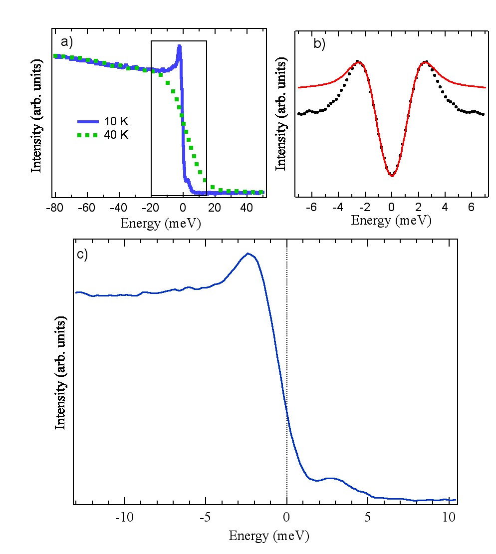
Given the above concern, we measured the energy gap in LuNi2B2C by partial angle-integrated photoelectron spectroscopy and compared with the normal state Fermi surface. The opening of the superconducting gap is clearly shown in Fig. 3. In order to determine the magnitude of the gap, the Dynes function Dynes1978 was fitted to the symmetrized Norman1998 spectrum (Fig. 3b). The fitted function yields the gap value of = 1.5 meV for the sample at T = 11 K with the parameter equal to 0.05 meV.
The striking feature in Fig. 3c is the pronounced peak above the chemical potential. This peak arises from thermal excitation of electrons above the 2. This points to high DOS just above which is consistent with the idea that the flat band along (110) direction, a large part of which is slightly over the Fermi energy playing an important role in this anisotropic superconductivity. Similar peaks were recently reported in Y based borocarbides YOKOYA2007 . According to BCS theory the energy gap value at zero temperature () is 2.45 meV for = 16 K superconductor. Our value of 1.5 meV obtained at T=11K corresponds to ()=2.6 meV, in excellent agreement with the BCS predictions.

IV Conclusions
We have performed measurements of the Fermi surface, band dispersion and supercondcuting gap for highest rare earth nickel borocarbide superconductor LuNi2B2C. The experimental data were compared with two different density functional calculations. The overall agreement between theory and measurement is good. In the experiment, large parallel FS parts spaced with the vector = 0.59a* have been found for two different incident photon energies, which is a confirmation of the previous theoretical predictions Rhee1995 and earlier experimental studies Dugdale1999 . The calculated FS confirms the existence of large nested parts, with a nesting vector in good agreement with the ARPES results presented here. The superconducting gap was measured and we also observed a coherent peak above the chemical potential. This peak arises due to electrons being thermally excited above the energy of 2.
V Acknowledgments
This work was supported by Director Office for Basic Energy Sciences, US DOE. Work at Ames Laboratory was supported by the Department of Energy - Basic Energy Sciences under Contract No. DE-AC02-07CH11358. Advanced Light Source is operated by the U.S. DOE under Contract No. DE-AC03-76SF00098. Synchrotron Radiation Center is supported by the National Science Foundation under award No. DMR-0537588. R. K. gratefully acknowledges support of K. Alex Müller Foundation.
References
- (1) R. J. Cava, H. Takagi, H. W. Zandbergen, J. J. Krajewski, W. F. Peck Jr, T. Siegrist, B. Batlogg, R. B. van Dover, R. J. Felder, K. Mizuhashi, J. O. Lee, H. Eisaki, and S. Uchida, Nature 367, 252 (1994).
- (2) R. Nagarajan, C. Mazumdar, Z. Hossain, S.K. Dhar, K. V. Gopalakrishnan, L. C. Gupta, C. Godart, B. D. Padalia, and R. Vijayaraghavan, Phys. Rev. Lett. 72, 274 (1994).
- (3) P. C. Canfield, P. L. Gammel, and D. J. Bishop, Physics Today 51, 40 (1998).
- (4) K.-H. Müller and V. N. Narozhnyi, Rep. Prog. Phys. 64, 943 (2001).
- (5) C. Mazumdar and R. Nagarajan, Current Science 88, 83 (2005).
- (6) T. Yokoya, T. Kiss, T. Watanabe, S. Shin, M. Nohara, H. Takagi, and T. Oguchi, Phys. Rev. Lett. 85, 4952 (2000).
- (7) E. Boaknin, R. W. Hill, C. Proust, C. Lupien, and L. Taillefer, Phys. Rev. Lett. 87, 237001 (2001).
- (8) N. L. Bobrov, S. I. Beloborod’ko, L. V. Tyutrina, I. K. Yanson, D. G. Naugle, and K. D. D. Rathnayaka, Phys. Rev. B 71, 014512 (2005).
- (9) K. Maki, P. Thalmeier, and H. Won, Phys. Rev. B 65, 140502 (2002).
- (10) P. Raychaudhuri, D. Jaiswal-Nagar, Goutam Sheet, S. Ramakrishnan, and H. Takeya, Phys. Rev. Lett. 93, 156802 (2004).
- (11) P. Martinez-Samper, H. Suderow, S. Vieira, J. P. Brison, N. Luchier, P. Lejay, and P. C. Canfield, Phys. Rev. B 67, 014526 (2003).
- (12) K. Izawa, K. Kamata, Y. Nakajima, Y. Matsuda, T. Watanabe, M. Nohara, H. Takagi, P. Thalmeier, and K. Maki, Phys. Rev. Lett. 89, 137006 (2002).
- (13) T. Siegrist, H. W. Zandbergen, R. J. Cava, J. J. Krajewski, and W. F. Peck Jr, Nature 367, 254 (1994).
- (14) L. F. Mattheiss, Phys. Rev. B 49, 13279 (1994).
- (15) W. E. Pickett and D. J. Singh, Phys. Rev. Lett. 72 , 3702 (1994).
- (16) R. Coehoorn, Physica C 228, 5671 (1994).
- (17) J. Y. Rhee, X. Wang, and B. N. Harmon, Phys. Rev. B 51, 15585 (1995).
- (18) H. Kim, C.-D. Hwang, and J. Ihm, Phys. Rev. B 52, 4592 (1995).
- (19) S. B. Dugdale, M. A. Alam, I. Wilkinson, R. J. Hughes, I. R. Fisher, P. C. Canfield, T. Jarlborg, and G. Santi, Phys. Rev. Lett. 83, 4824 (1999).
- (20) P. Dervenagas, M. Bullock, J. Zarestky, P. Canfield, B. K. Cho, B. Harmon, A. I. Goldman, and C. Stassis, Phys. Rev. B 52, 9839 (1995).
- (21) P. C. Canfield, I. R. Fisher, J. Crystal Growth, 225, 155-161 (2001) .
- (22) O. Jepsen and O. K. Anderson, Solid State Commun. 9, 1763 (1971) and Phys. Rev. B 29, 5965 (1984); P. Blöchl, O. Jepsen and O. K. Anderson, Phys. Rev. B 49, 16223 (1994).
- (23) P. Blaha, K. Schwarz, G. Madsen, D. Kvasnicka and J. Luitz, (2001) WIEN2k, An Augmented Plane Wave + Local Orbitals Program for Calculating Crystal Properties (Karlheinz Schwarz, Tech. Univ. Wien, Austria).
- (24) S. Hufner, Photoelectron Spectroscopy, pp 268-270 (Springer, Berlin 1995).
- (25) R. C. Dynes, V. Narayanamurti, and J. P. Garno, Phys. Rev. Lett. 41, 1509 (1978).
- (26) M. R. Norman, H. Ding, M. Randeria, J. C. Campuzano, T. Yokoya, T. Takeuchi, T. Takahashi, T. Mochiku, K. Kadowaki, P. Guptasarma, and D. G. Hinks, Nature 392, 157 (1998).
- (27) T. Baba, T. Yokoya, S. Tsuda, T. Kiss, T. Shimojima, K. Ishizaka, H. Takeya, K. Hirata, T. Watanabe, M. Nohara, H. Takagi, N. Nakai, K. Machida, T. Togashi, S. Watanabe, X.-Y. Wang, C. T. Chen, and S. Shin, Phys. Rev. Lett. 100, 017003 (2008).