Measurement of Coulomb drag between Anderson insulators
Abstract
We report observations of the Coulomb drag effect between two effectively 2-d insulating a-Si1-xNbx films. We find that there only exist a limited range of experimental parameters over which we can measure a sizable linear-response transresistivity (). The temperature dependence of is consistent with the layers being Efros-Shklovskii Anderson insulators provided that a 3-d density of states and a localization length smaller than that obtained from the DC layer-conductivity are assumed.
Materials such as a-Si1-xNbx which exhibit a disorder driven (Quantum Critical) Metal-Insulator Transition (MIT) sgc97 ; bsd85lcb98 have presented many challenges to condensed matter physics: in particular understanding the role of long ranged electron-electron interactions in the insulating phases hgc01 and in the vicinity of the MIT bsd85lcb98 . Since the interplay between disorder and electron-electron interactions in such systems will determine the dominant transport mechanism, the development of experimental techniques to separately measure these is useful. In this letter we show that the Coulomb drag effect allows us to directly study long ranged electron-electron interactions in insulating a-Si1-xNbx thin films. We find that although linear-response Coulomb drag is only observable over a limited range of sample parameters, when obtainable, it offers unequivocal distinction to be made between alternative models for the electronic transport in such systems.
Coulomb drag spf89 arises from the Coulomb scattering of charge carriers in spatially separated layers, in the absence of charge transfer between the layers. Experimentally, the Coulomb drag effect between two layers (layer- and ) can be observed by measuring the electric-field () created in one, open circuited, layer due to a parallel applied current-density () in the other. The (longitudinal) transresistivity, or linear-response Coulomb drag coefficient, is defined as ; whilst the measured total-transresistance is the ratio of the induced voltage in layer-2 to the applied current in layer-1, i.e. . Theoretical analyses agree that the linear-response transresistivity between two identical 2-d layers is given by, e.g. zm93 :
| (1) |
where , is the temperature, is the carrier density in a layer, is the density-density response function of a layer, and is the screened interaction potential between the layers. may be obtained from the finite wavevector conductivity via:
| (2) |
The motivation for this study comes from predictions s97 that the temperature dependence of the transresistance can be used to differentiate insulating states. In particular, for the case of (2-d) Mott Anderson insulator bilayers the low- transresistivity should vary as , whilst for (2-d) Efros-Shklovskii(ES) Anderson insulators it should diverge when as , where is the ES characteristic temperature given by and is the dielectric constant of the layers. This opposite behavior of the transresistivity as (diverging for ES-Anderson insulator bilayers, and vanishing for Mott Anderson insulator bilayers) allows for a more transparent distinction between the two insulating states over a narrow range than intra-layer transport measurements do—where one would obtain different functional or dependencies with the same trend.
In our study, samples consisted of two U-shaped 200Å thick insulating a-Si1-xNbx layers, separated by a SiO barrier (see upper left inset in figure 2). All layers were fabricated using standard RF magnetron sputtering techniques, with the a-Si1-xNbx layers being deposited using the co-sputtering technique with a rotating sample-holder outlined in Refhgc01 . Samples were all grown on polished glass slides in an inert (argon) environment at ambient temperature and a pressure of kPa. Prior to the layers being deposited, Å-thick silver connections and a silver bridge, that would connect the two layers, were sputtered. The latter would prevent the barrier from breaking due to electrostatic discharge/breakdown during handling, characterization and cooling. Connections to the signal generating and measuring apparatus were made with sputtered silver layers on the arms of the U-shaped layers several millimeters from the interacting-region. To prevent oxidation the top layer was covered with a 50Å-thick SiO film prior to atmospheric exposure. Thicknesses were inferred from the sputtering rate (measured using a quartz crystal thickness monitor), and were within of those obtained from optical interferometry measurements on samples of similar compositions and thicknesses. Estimates of the uncertainty in the thickness due to fluctuations in the deposition rate and uncertainties in the exposure time are Å and Å for the case of the a-Si1-xNbx and the barrier layers respectively. The barrier layer was deposited in discrete stages to reduce the formation of pinholes. High sputtering powers and brief atmospheric exposure between stages were found to increase the barrier strength and durability. We were thereby able to fabricate barrier layers with resistances several orders of magnitude larger than those of the layers.
Samples were cooled to K using a standard liquid helium cryostat. The low- (20K) resistance of the barrier layer was obtained by measuring its conductance, i.e. by applying a small DC potential difference between terminals on either layer, and then measuring the induced current. Measurements were performed from several terminals on each layer and with various terminals and connections grounded to rule out any effects from ground-leakage and -loops. Single layer resistance measurements were performed using standard 4-wire techniques, for which it was assured that driving currents were small enough to give linear-response coefficients. The indifference of the layer resistances to the grounding of terminals in the second layer provided further verification that inter-layer leakage and tunneling was not significant. Transresistance measurements were performed using a quasi-AC technique in which a DC current source was programmed to flip polarity every 1 second. Since in linear-response theory remains the same on interchanging the layers (even if the layers have different resistivities), the condition that (/square)2→1 = (/square)1→2 as the driving-current is decreased, was used as a test for the linear-response regime.
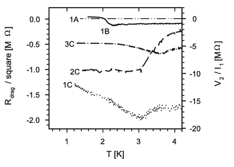
The transresistance at driving currents of nA for samples with average Nb concentrations per layer niobiumconc of and layer separations of Å were found to, on average, increase with decreasing temperature between K. At lower temperatures the transresistance would saturate or decrease in magnitude. This is shown in figure 1 for a selection of samples. In what follows we will present data for sample 1B, where the transresistance entered the linear-response regime for nA. Due to the multitude of competing size effects (see below), it was unclear, based on the temperature dependence of the DC resistance alone, whether the layers are better described by the ES Variable Range Hopping(VRH) model es75 , which predicts: , or the Mott VRH model m70 , which, for effectively 2-d films, predicts: , at low temperatures. This can be seen in figure 2, where we present and plots of the layer-resistances of sample 1B. In the temperature range K, ES VRH with a characteristic temperature of K, 2-d Mott VRH with a characteristic temperature of K, and 3-d Mott VRH with a characteristic temperature of K, all describe the -dependence reasonably well. The localization length determined from the ES characteristic temperature is Å.
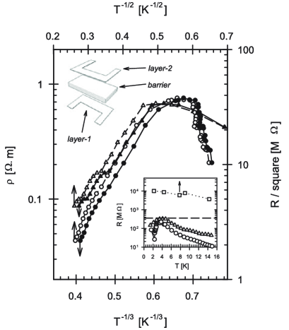
For each case the DC VRH transport in the layers should be effectively 2-d for T20K—on account of the resonant hopping distance () being larger than the width of each layer (). At these temperatures the resistance of the barrier—obtained by measuring the tunneling current (see above)—is found to be approximately two orders of magnitude larger than the resistance of layers-1 and -2 (see lower inset in figure 2).
The observed decrease of the layer-resistance and transresistance observed at T2.5K is (based on the tests outlined above and in Refgem91 ) neither due to grounding loops/leaks or tunneling/leakage through the barrier. It is unlikely that they are due to thermoelectric effects (as in e.g. spf89 ), given that all connections were far away from the interacting region. Furthermore, it is unlikely to be due to the layers undergoing a superconductor-insulator transition—which is known to occur in thin a-Si1-xNbx films with large Nb concentrations ( amp06 )—based on the high resistance per square of the layers and the high temperature at which the transition appears to occur. We will present a comprehensive study of this phenomenon elsewhere, and focus on the temperature range K in this letter.
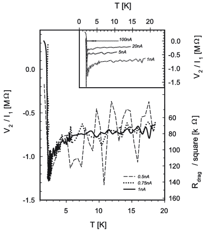
As the driving current is increased the transresistance decreases (see inset in figure 3), and for nA, the transresistance is found to be more than orders of magnitude smaller than at nA. This is likely due to larger driving currents both increasing the effective sample temperature and producing significant non-linear responses. For nA the drag voltage becomes noisier, but its average value changes by less than between , and nA (see figure 3). We thus believe that at this point we have reached the linear-response regime. It is unlikely that phonon gem93 and plasmon fh94 contributions are significant at these temperatures on account of the small layer separations and the strong insulating nature of the layers.
In order to limit the number of fitting parameters in analysing these data, we find it convenient to plot the ratio (/square)/(/square) as a function of temperature. Doing so we find that our data is best described (see figure 4) by the 2-parameter equation: (/square)/square), with K-b and .
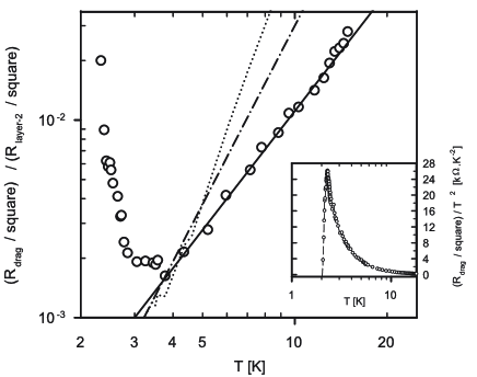
The latter parameter deviates from the predictions of Refs97 , which suggest that for a bilayer system comprised of 2-d ES Anderson insulators.
The observed discrepancy can be explained if the screening in the layers is not 2-d in the studied regime—i.e. if the response is dominated by a finite wave-vector (where Å) for which the layers will be effectively 3-d. Since , at the temperatures of interest, this occurs at momentum transfers () that dominate the transresistance (see Refs97 ).
Repeating the calculations for the finite- conductivity in Refas94 for 3-d systems, we find it takes the asymptotic forms:
| (3) |
| (4) |
where ,
, and , are
numerical constants of order unity. Substituting
equations (3) and (4) into
(2) and then (1), we find that the
dominant contribution to the transresistance, if the layers are
treated as effectively 3-d for and we can
assume weak static screening, would change with as:
. The
observed
temperature dependence can however arise if one or both of the
following are the case:
(1) The relevant localization length is much smaller than
that obtained from the -dependence of the DC conductivity so
that:
| (5) |
In this way the momentum transfers (which are
otherwise dominant) are suppressed, and the
contribution determines the low- transresistance. Substituting
equation (4) into (2) and
(1), the transresistance would now change with temperature
as: .
(2) Finite- transport is effectively 3-d due to
pair-arms () reaching into the barrier and the second
layer. From the strongly localized nature of electrons in the
barrier layer, the effective would be much smaller and
condition (5) may be satisfied, even if the effective
layer separation also decreases significantly.
We note that since several of the relevant length scales are comparable (), a small modification of the effective values that these parameters take (due to e.g. finite-size effects, correlated hopping or surface effects) could cause a change between the and regime in the temperature range probed, resulting in a different -dependence than that predicted. We also note that we do not observe the expected transition from the to the regime, as the temperature is increased. However, if the apparent change in the -dependence of the transresistance (see figure 4) at T4K occurs when the regime kicks in, then we predict that Å. This would give a transresistance that goes as for K, or , as we have observed.
In conclusion, we have observed the Coulomb drag effect between two Å thick insulating a-Si1-xNbx films (with ) separated by a Å thick SiO based barrier. We were able to retrieve accurate linear-response data for , and layer separations of Å. The temperature dependence of the transresistance in such samples was found to be in agreement with that predicted for ES Anderson Insulator films, provided that the localization length in the a-Si1-xNbx layers is smaller than that inferred from the temperature dependence of the DC layer-resistances. Our study suggests that whilst theoretically the Coulomb drag effect is a useful technique for distinguishing the insulating states of thin films, it is experimentally challenging due to the complex dielectric properties of disordered thin films at low energies, which result in non-linear inter- and intra- layer excitations becoming dominant at practical temperatures and sample dimensions. Experimental studies of the non-linear crosstalk regime between thin insulating films, along with simulations of the non-linear (current-dependent) transresistance in such systems, may prove to be the most productive method of studying the detailed nature of the observed excitations.
Acknowledgements.
We would like to thank Prof. E. Shimshoni for fruitful discussions, and D. Sprinkle and M. Hosek for help with the experiments.References
- (1) S.L. Sondhi, S.M. Girvin, J.P. Carini, and D. Shahar, Rev. Mod. Phys. 69, 315 (1997).
- (2) D.J. Bishop, E.G. Spencer, and R.C. Dynes, Solid State Electron. 28, 73 (1985); H.-L. Lee, J.P. Carini, D.V. Baxter, W. Henderson, and G. Grüner, Science 287, 633 (2000).
- (3) E. Helgren, G. Grüner, M.R. Ciofalo, D.V. Baxter, and J.P. Carini, Phys. Rev. Lett. 87, 116602 (2001).
- (4) P.M. Solomon, P.J. Price, D.J. Frank, and D.C. La Tulipe, Phys. Rev. Lett. 63, 2508 (1989).
- (5) L. Zheng and A.H. MacDonald, Phys. Rev. B 48, 8203 (1993).
- (6) E. Shimshoni, Phys. Rev. B 56, 13301 (1997).
- (7) Average niobium concentrations were estimated by comparison of the deposition rate and characteristic ES and Mott temperatures to that of a-Si1-xNbx films for which was determined from Electron microprobe analysis.
- (8) A.L. Efros and B.I. Shklovskii, J. Phys. C: Solid State Phys. 8, L49 (1975).
- (9) N.F. Mott, Phil. Mag. 22, 7 (1970).
- (10) H. Aubin, C.A. Marrache-Kikuchi, A. Pourret, K. Behnia, L. Berge, L. Dumoulin, and J. Lesueur, Phys. Rev. B 73, 094521 (2006).
- (11) T.J. Gramila, J.P. Eisenstein, A.H. MacDonald, L.N. Pfeiffer, and K.W. West, Phys. Rev. Lett. 66, 1216 (1991).
- (12) T.J. Gramila, J.P. Eisenstein, A.H. Macdonald, L.N. Pfeiffer, and K.W. West, Phys. Rev. Lett. 47, 12957 (1993).
- (13) K. Flensberg and B. Y-K. Hu, Phys. Rev. Lett. 73, 3572 (1994).
- (14) I.L. Aleiner and B.I. Shklovskii, Intern. Journ. of Mod. Phys. B 8, 801 (1994).