, ,
Electronic and Optical Properties of Electromigrated Molecular Junctions
Abstract
Electromigrated nanoscale junctions have proven very useful for studying electronic transport at the single-molecule scale. However, confirming that conduction is through precisely the molecule of interest and not some contaminant or metal nanoparticle has remained a persistent challenge, typically requiring a statistical analysis of many devices. We review how transport mechanisms in both purely electronic and optical measurements can be used to infer information about the nanoscale junction configuration. The electronic response to optical excitation is particularly revealing. We briefly discuss surface-enhanced Raman spectroscopy on such junctions, and present new results showing that currents due to optical rectification can provide a means of estimating the local electric field at the junction due to illumination.
1 Introduction
Electronic devices with molecules and organic components as active elements offer new limits of device scaling and functionality, and are also of fundamental physical interest. Studies at the single molecule level probe the physics of electronic conduction and optical interactions in regimes that have been previously inaccessible. Three-terminal electronic measurements have proven invaluable in many systems, enabling electronic transport to function as a spectroscopy of available states.[1] While much progress has been made using two-terminal measurements to examine charge transport through molecules[2, 3, 4, 5, 6, 7, 8, 9, 10, 11, 12, 13, 14, 15, 16, 17, 18, 19, 20] , three-terminal measurements greatly increase the available information in single-molecule measurements. For example, through the use of a gate electrode it is possible to study conduction as a function of the molecule’s redox potential, analogous to what can be done in electrochemical experiments.
A common approach to fabricating three-terminal single-molecule devices is known as the “electromigration technique”, in which thermally assisted electromigration is used to create a nanoscale gap in a narrow metallic wire situated on a gate insulator material[21]. If a molecule of interest resides in the nanogap, the broken ends of the wires are used as the source and drain contact electrodes, and an underlying conductive substrate can be used as a gate electrode. The resulting device is a single-molecule transistor (SMT). Electromigrated breakjunctions have been used to study transport through individual nanocrystals[21], small metal particles[22], a variety of molecules[23, 24, 25, 26, 27, 28, 29, 30, 31, 32, 33, 34, 35, 36, 37, 38, 39], and even individual atoms[40].
A central hurdle in most single-molecule electronic measurements is to demonstrate unambiguously that transport is occurring through only a single molecule of interest. This is complicated by the lack of direct imaging techniques with sufficient resolution, except for the two-terminal example of scanning tunneling microscopy (STM), which allows imaging with atomic resolution on conducting substrates. In this paper we review SMT fabrication (Section 2), and then discuss device characterization based on electronic transport alone as a diagnostic (Section 3). In that circumstance it is necessary to search for features characteristic of conduction through a single molecule in addition to attributes uniquely identifying the molecule of interest. Generally the search for single molecule devices requires a statistical approach and many control experiments. Exciting recent work (Section 4) demonstrates that simultaneous single-molecule optical spectroscopy and transport is possible. In such measurements surface-enhanced Raman spectroscopy (SERS) can give the vibrational spectrum of the specific molecule through which transport is taking place. We present new data using nonlinear transport and optical rectification to arrive at a quantitative estimate for the local optical field experienced by the molecule under illumination.
2 Device Fabrication
Fabrication begins with the preparation of arrays of devices on an Si substrate with a 200 nm SiO2 insulating layer. 1 nm of Ti and 15 nm of Au are evaporated onto nanowire patterns defined by electron beam lithography. Bowtie-shaped constriction patterns are produced with minimum widths of approximately 100 nm (Figure 1a). Additional gold pads for contacting the source and drain electrodes are also defined by electron beam lithography. The array of samples is cleaned in solvents then exposed to an oxygen plasma for 1 min to remove trace organics. The molecules are dispersed for approximately monolayer coverage, or allowed to self-assemble onto the Au surface, depending on the molecule in question.
Electromigration (with some thermal enhancement due to Joule heating) is used to break the constriction into distinct source and drain electrodes, with the intent that the molecule will reside in the resulting nanoscale gap. This process has been studied extensively by a number of investigators[41, 42, 43, 44, 45, 46]. At large current densities in the constriction, the electrons transfer sufficient momentum to the lattice to move atoms at the surface and at grain boundaries. As a constriction is formed the local current density increases, leading to a runaway migration and the formation of an interelectrode gap. Elevated local temperatures enhance the rate of this process through the increased diffusion of metal atoms. To mitigate concerns about adsorbed contaminants we prefer to electromigrate junctions at low temperatures in a cryopumped ultrahigh vacuum (UHV) environment, though this has not been possible in the optical experiments discussed in Section 4. The critical gap size, defined as the minimum separation between the two resulting electrodes, is typically 1-3 nm. With good, reproducible lithography to produce the constrictions and an appropriate electromigration procedure, yields of such small gaps can exceed 90%.
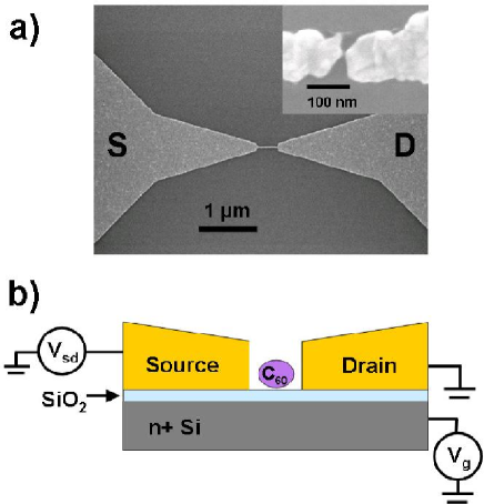
An assortment of voltage ramping techniques have been utilized by different research groups in an effort to form the smallest, cleanest, and most consistently-sized nanogaps[41, 42, 43, 44, 45, 46]. All techniques involve minimizing the series resistance to avoid overheating and subsequent melting of a nanowire; and an immediate reduction in applied bias across the break after the gap has opened in order to avoid creating an excessively large interelectrode spacing. We have found success with a feedback controlled method of repeatedly ramping the source-drain voltage, .
The desired final device configuration is shown schematically in Figure 1b. Subtle differences in junction configuration down to the Ångström level can strongly influence device properties. The WKB approximation dictates that the current through a metal-vacuum-metal gap decreases by roughly a factor of (7.4) for every Ångström increase in the size of the vacuum gap[49]. This exponential dependence of tunneling on interelectrode distance ensures, as in an STM, that the tunneling electrons probe a volume containing at most one or two molecules. Precisely how molecules that begin on the surface of the constriction end up in the interelectrode gap is not known. The inherent randomness in the device formation process leads to many electrode-molecule configurations and resulting electrical conduction characteristics for any group of devices. Historically this has mandated a statistical approach to device characterization based on transport. By analysis of the transport data, as explained below, it is often possible to infer the number of molecules in the tunneling region and the relative couplings of the molecule to the source and drain electrodes. Details about molecular positioning and bonding remains unavailable, though new measurements such as those in Sect. 4 contain much information.
3 Low temperature electronic transport
The differential conductance, , as a function of , calculated or measured using quasi-dc techniques, is the main transport tool to assess the nature of a given device. There are four main classes of differential conductance traces, with characteristic abundances determined by examining large numbers (thousands) of junctions[37] (though these vary depending on molecule type). 1) Devices with no measurable differential conductance indicate an interelectrode breakjunction gap that is too large for measurable conduction by tunneling (%). 2) Devices with a weakly nonlinear conductance plot wherein drops around = 0, but does not form a clear blockaded region denote breakjunctions with small to moderately sized gaps, but without an active element within the nanogap (Figure 2a, %). 3) Devices that show a region of zero conductance bordered by sharp peaks most likely have a gap containing a molecule or small particle (Figure 2b, percentage depends strongly on molecule type). 4) Devices with a zero-bias resonance suggest a stronger molecule-electrode coupling (percentage depends strongly on molecule type, ranging from zero for alkane chains to several percent for transition metal complexes containing unpaired electrons[31]).
Further investigation is required to identify those devices that contain a single molecule of interest. Confounding possibilities include surface contaminants, metal grains produced during the electromigration process, or simply more than one molecule of interest. As explained below, the observed gate dependence of conduction and an understanding of the relevant transport physics has enabled progress in eliminating spurious devices. The final yield of gateable likely SMTs is typically 10-15% of the starting devices, based on a total sample size of thousands of devices.
3.1 Coulomb blockade
In analogy to conventional single-electron transistors, the SMT can be thought of as consisting of 6 parts: source, drain and gate electrodes, the molecule, and the tunneling connections to the source and drain. The tunneling barriers are established by the geometry and chemistry of the molecule/electrode interface. We assume that the polarizability of the complex is much larger than that of the insulating barriers; therefore the voltage drops on the barriers are proportional to their respective coupling strengths and . Elementary transport characteristics can be calculated by treating tunneling barriers as a capacitive and a resistive element[50]. The positive and negative slopes of the blockaded region (the tunneling thresholds) are determined by the ratios and , respectively[30] (, , and are the capacitances between the molecule-gate, molecule-drain, and molecule-source electrodes).
Traces of measured as a function of , obtained within a range of incrementally changing gate voltage, , can be compiled to form a map known as a stability diagram, illustrating where tunneling is both allowed and prohibited. Not all devices exhibiting a zero-bias resonance or a conductance gap will show dependence on applied gate bias, . This poor gate coupling may occur as a result of the detailed device geometry or possibly as a result of the orientation of the active element within the breakjunction gap[31, 51]. Stability diagrams of devices that do exhibit gate dependence are a primary means of displaying pertinent transport data reflecting important aspects of SMT behavior.
In equilibrium the source and drain electrodes have a common electrochemical potential, , the Fermi level. When the source and drain electrodes are biased such that the source electrode has a chemical potential and the drain electrode has chemical potential , current will flow as long as the Coulomb charging energy () and the discrete energy level spacing () have been overcome, and an energy level of the molecule lies between and (at finite temp, this range is extended by the thermal energy [52]). This current flow is due to resonant tunneling of electrons from the source to the lowest available single particle state producing a peak at the edge of the conductance gap (Figure 3c). Gate voltage shifts the active element levels with respect to and . The resulting stability diagram is determined by both the active element’s spectrum and its capacitive couplings to the source, drain, and gate electrodes.
When the active element has a negligible single-particle level spacing (e.g., a few-nm metal grain), the discrete spectrum seen in transport arises purely from , the Coulomb repulsion that must be overcome to add another electron to the element. The result is a series of regularly spaced diamonds in the stability diagram, and the suppressed conduction in the absence of a discrete level available for transport is called Coulomb blockade. Each diamond region represents a different charge state of the particle (i.e. a stable region of fixed average electron number). In this case the electron addition energy depends upon the classical capacitance of the particle, including interactions with the electrodes.
Frequently the single-particle electronic level spacing, , cannot be neglected when considering transport. If the island is a molecule such as C60, the discrete energy level spacing between single particle energy states at equilibrium occurs between the highest occupied molecular orbital level (HOMO level) and the lowest unoccupied molecule orbital level (LUMO level), commonly called the HOMO-LUMO gap. We can see from equation (1) that the size of the Coulomb diamond centered around depends on both the Coulomb charging energy as well as the magnitude of the HOMO-LUMO gap.
| (1) |
where , is the slope of the diamonds, and is the voltage spacing between successive charge states.
| (2) |
where is the spacing between two discrete energy levels (e.g. the HOMO-LUMO gap), and is the bare Coulomb charging energy, .
Unlike metal particles, most molecules have a very limited number of accessible charge states, which do not typically appear with even spacing. Solution-based electrochemistry (e.g. cyclic voltammetry) demonstrates that molecules have a limited number of accessible valence states.[37] If one finds that it is possible to add many electrons to a potential device via gating, or if the spacing between charge state transitions is highly regular, it is extremely unlikely that the active region of the potential device contains a single small molecule.
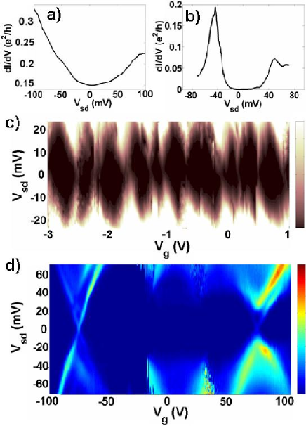
Stability diagrams with linear tunneling barrier edges possessing only two characteristic slopes (one positive and one negative) can be simulated using the basic capacitance model of sequential electron tunneling[36]. A system with more that one active element will always have more than two characteristic slopes. This provides a means of assessing whether tunneling is occurring through multiple molecules.
When scrutinizing a potential SMT with a clear blockaded region, one must also look at the electron addition energy (the max source-drain bias of the blockaded region), which should be of a sensible size for the molecule in question. The classical capacitance of a molecule is so small that an electrostatic charging energy over 100 meV is not unreasonable, even without taking into account molecular level spacing.
Some characteristics in stability diagrams may uniquely identify an SMT made with a particular molecule. At sufficiently high source drain bias, an electron may tunnel from the source into an excited single particle state of the island (Figure 3d). Additional peaks that parallel the edges of the blockaded diamonds in stability diagrams appear beyond the edge of the conductance gap when tunneling occurs through newly accessible quantized excitations. The location of each peak outside the conductance gap provides information on the excitation spectrum of a SMT.
The conductance gap disappears (ordinarily) at the charge degeneracy point, , where the total energy of the system is the same for two different charge states of the molecule. When the gate voltage passes Vc as it is ramped in the positive direction, the average number of charges on the molecule changes by one electron. The absolute equilibrium electron population, , is determined by , molecule/electrode interfacial charge transfer, and the local charge distribution around the molecule. Unfortunately, cannot be determined solely from the data obtained in the stability diagram.
Each peak on the side of a stability diagram represents an opening of a new tunneling pathway where an electron tunnels onto the -electron state, for example, to transiently generate the -electron ground or excited states. In this way, the peaks probe the excitation energies of the molecule. Conversely, each peak that appears at probes the ground and excited states of the -electron molecule[24]. The energy of these quantized excitations can be determined from the source/drain voltage at which they intercept the conductance gap. If these excitations can be identified with known molecular properties, they can serve as a fingerprint for molecular identification.
Higher-order tunneling events known as cotunneling may be observed inside the Coulomb blockade region of an SMT when the overall tunneling current is very small. Cotunneling becomes more apparent as the coupling between the dot and leads is enhanced, and can give rise to the non-zero current inside the blockaded region. Elastic cotunneling corresponds to an electron tunneling into and out of the same energy level, such that the molecule remains in its ground state (Fig 3e). Inelastic cotunneling occurs when an electron enters and exits the molecule through two different energy levels, ultimately leaving the molecule in an excited state. When , where is the energy level spacing between the ground state and the first excited state, inelastic cotunneling processes can occur (Figure 3f)[53, 54]. Cotunneling events are only weakly affected by and can be most clearly seen in a stability diagram mapping . Vibrational inelastic cotunneling is equivalent to inelastic electron tunneling spectroscopy[28].
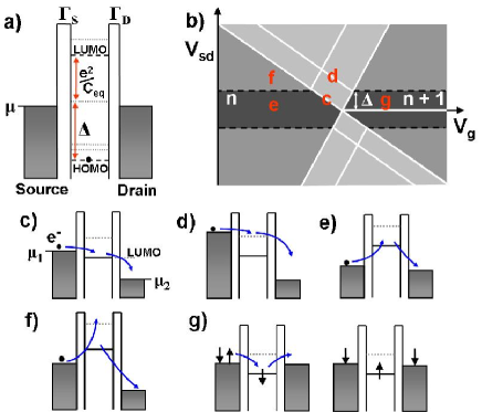
Excited states can originate from several possible degrees of freedom, including excited electronic states of the system and, in molecules, internal vibrational modes. If the pattern of excitations is identical for multiple charge states of a given molecule (i.e. excitation are observed on both sides of at the same value of ) this suggests that the excitations are not associated with molecular charge states and are therefore independent of the electronic configuration. Additionally, if excitation energies are equally spaced then their origin is also unlikely to be excited electronic charge states.
As long as the exact structure of a molecule is known, its vibrational modes can be computed, and further calculations can demonstrate that only some of these modes are plausible candidates for excitation peaks observed in stability diagrams.[55] For instance, experimental and theoretical studies of C60 show that the lowest energy internal vibrational mode energy 33 meV and corresponds to the deformation of the Buckminsterfullerene sphere into a prolate ellipsoid.[23] Similar considerations have been used to distinguish a known vibrational mode in C140.[29] In addition it is also possible to excite a center-of-mass oscillation of a molecule (commonly known as the bouncing ball mode) within the confinement potential that binds it to the electrode surface[23].
An additional higher-order tunneling process that is apparent in many SMT devices is the formation of a many-body Kondo resonance. This phenomenon has studied in semiconductor quantum dots[56, 57, 58] and SMTs[24, 25, 26, 27, 31, 37]. Observing the Kondo effect requires an unpaired electron to exist in the active element. In the framework of the Anderson single level impurity model, the active element is then an effective magnetic impurity[59] with the singly occupied level’s energy, , below the source/drain Fermi level (Figure 4a). Because of the Coulomb interaction, it is classically forbidden to bring the electron out of the impurity without adding energy into the system. However, higher order tunneling processes can take place such that another electron from the source/drain electrode Fermi sea may exchange with the local moment. At low temperatures the coherent superposition of all possible cotunneling events results in the screening of the local spin; the resulting ground state is a correlated many-body singlet state spanning the source, impurity, and drain. This Kondo resonance is manifested as a conductance peak at the Fermi energy ().
The Kondo temperature, , is the characteristic temperature associated with the formation of the Kondo singlet. The characteristic energy scale is exponentially dependent on , the intrinsic width of the single particle level, by the relation[60]
| (3) |
outside the mixed valence regime (). The total width is dictated by the overlap between the single particle state and the conduction electron states of the source and drain. Therefore is in turn exponentially sensitive to the precise molecule-electrode configuration. This indicates both that a Kondo resonance will only be found in devices with relatively strong molecule-electrode coupling, and for SMTs displaying a Kondo resonance, the overall conductance level will be significantly increased with respect to similar SMTs in the Coulomb blockade regime. In a symmetric system, as , the SMT will approach its theoretical maximum conductance . It is possible that a relatively high Kondo temperature can be associated with a device exhibiting a lower conductance as the total conductance is determined by the smaller of and while is determined by the total .
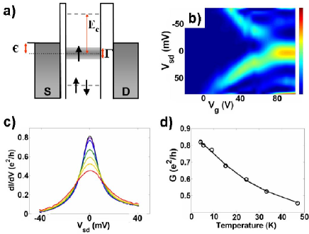
The Kondo resonance will decrease in magnitude and increase in width as temperature is increased. A fit to the semiempirical expression for the spin- Kondo resonance related to maximum conductance,
| (4) |
where , or to the full width at half max
| (5) |
allows extraction of the corresponding Kondo temperature, . Measurements of or FWHM as a function of that cannot be fit to these expressions likely indicate a zero-bias resonance that does not originate from a Kondo state. Zeeman splitting of the zero-bias resonance in an applied magnetic field can also be used to determine the magnetic nature of molecular state, and hence to corroborate the presence of a Kondo state. Finally, we always attempt to verify that the measured stability diagrams can be seen to transition from the Kondo regime to the Coulomb blockade regime. This evidence that charge state of the device can be altered with the gate together with the data from the tunneling thresholds of the potential SMT in the Coulomb regime will further attest to the nature of the device.
The Kondo effect can be an additional “fingerprint” used to identify molecular states. Gate dependence of the Kondo resonance in SMTs has proven to be weaker than that seen in semiconductor dots[31], and “satellite” peaks associated with Kondo physics in the presence of molecular vibrations have been observed[26, 31, 61]. Also, since only odd occupancy charge states can exhibit the Kondo effect, the presence of a zero-bias resonance can be used to help identify specific charge states. Care must still be exercised, however: Zero-bias resonances that do not result from the Kondo effect may occur in some devices, while devices believed to contain metal nanoclusters[47] can exhibit the Kondo effect in the absence of molecules.
4 Optical effects in electromigrated nanogaps
Combined optical and transport experiments on electromigrated nanogaps can reveal a wealth of additional information beyond that available in purely electronic measurements. The same source/drain electrodes used to couple current to the nanogap are observed to act as tremendously effective plasmonic antennas, leading to dramatic surface enhanced Raman scattering (SERS) in the junctions[62, 63]. Here we describe recent results in combining SERS and transport measurements, and report an additional effect: optical production of dc electrical currents in these molecular nanogap systems. These currents are consistent with optical rectification due to nonlinearity of the electromigrated junction’s conduction, and provide a means of estimating the magnitude of the enhanced optical fields in the junction region.
4.1 Surface-enhanced Raman scattering
We have performed a series of optical measurements of Au nanogap structures (prepared as in Section 2) using a WITec CRM 200 Confocal Raman microscope. Measurements were made with a 785 nm diode laser with an incident power of 0.5 mW, chosen to maximize signal, minimize photodamage to assembled molecules, and avoid thermally driven rearrangement of the nanogap electrodes. All optical measurements were performed at room temperature in air. Nanogap devices were located in the microscope by rastering the sample beneath the microscope objective to create a spatial map of the Raman response with step sizes as small as 10 nm. The Si substrate’s strong 520 cm-1 Raman peak can be used to map out the position of nanogap since the Au film of the electrodes attenuates the Si Raman response. Once the nanogap was located, Raman spectra were taken with 1-2 s integration time periods to study the dynamics of the nanogap system.
Initial experiments examined nanogaps as a potential surface-enhanced Raman spectroscopy (SERS) substrate[62], with para-mercaptoaniline (pMA) as the molecule of interest. Nanoconstrictions were placed in parallel to allow simultaneous electromigration of seven nanogaps at one time. Samples were characterized in the Raman microscope via spatial maps and time spectra of the SERS response. Prior to electromigration, no significant SERS response is detected anywhere on the devices.
Following electromigration, we observe a SERS response strongly localized to the resulting gaps. Successive spectra measured directly over the SERS hotspot revealed “blinking” and spectral diffusion, phenomena often associated with single- or few-molecule Raman sensitivity. Blinking occurs when the Raman spectrum rapidly changes on the second time scale with the amplitudes of different modes changing independently of one another. Spectral shifts as large as cm-1 were observed, making it difficult to directly compare SERS spectra with other published results. Blinking and spectral shifts are attributed to movement or rearrangement of the molecule relative to the metallic substrate. It is unlikely that an ensemble of molecules would experience the same rearrangements synchronously and thus blinking and wandering are expected to be observed only in situations where a few molecules are probed.
More recently, we have performed simultaneous SERS and transport measurements[63], including Raman microscope observations over the center of nanogap devices during electromigration. Molecules of interest, pMA or a fluorinated oligimer (FOPE), were assembled on the Au surface prior to electromigration. A 100 ultra-long working distance objective was used to allow electrical probes to be placed beneath the objective to make contact with the nanogap source and drain electrodes. The nanogaps were migrated in situ using a computer controlled DAQ. Transport measurements were made by sourcing a 50-100 mV RMS sine wave at 200 Hz using a SRS 830 lock-in amplifer into one electrode, with a Keithley 428 current-to-voltage amplifier connected at the other electrode. The ac current and its second harmonic were measured with lock-in amplifiers and the dc current was measured at 5.0 kHz using a DAQ. Simultaneously Raman spectra were acquired with a 1 s integration time.
Optical measurements during electromigration provide a wealth of information about the plasmonic properties of nanogaps. Once the device resistance exceeds approximately 1 k, SERS can be seen. This indicates that localized plasmon modes responsible for the large SERS enhancements may now be excited. As the gap further migrates the SERS response is seen to scale logarithmically with the device resistance until the resistance reaches approximately 1 M. In most samples the Raman response and conduction of the nanogap become decoupled at this point with the conduction typically changing little while uncorrelated Raman blinking occurs. A more extensive discussion of the connection between plasmonic modes and interelectrode conductance is presented elsewhere[63].
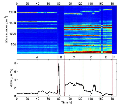
In about 11% of 190 devices, however, the Raman response and conduction show very strong temporal correlations. The 11% yield is is quantitatively consistent with yields of gateable SMTs as mentioned in Section 3. A typical correlated SERS time spectrum and conductance measurement for a FOPE device are presented in figure 5. The temporal correlations between SERS and conduction are clear. In region A we observe a stable Raman spectrum and small conductance changes which appear to be correlated with changes in the Raman mode at 1980 cm-1. After a short spike in conductance the conductance and Raman disappear at B. In section C the conductance and Raman spectrum return. This time the conductance is 6x larger than in A and the Raman modes are different. In particular the mode previously seen at 1980 cm-1 is now at 1933 cm-1. In region D we see the conductance drop to levels closer to those seen at A and the 1933 cm-1 mode from C shifts to 2038 cm-1. During D we see that the conductance momentarily returns to the value seen in section C correlated with a shift in the 2038 cm-1 mode back to 1933 cm-1. In section E we see another shift in position of the 1933 cm-1 mode to 2098 cm-1 which slowly shifts up to 2122 cm-1. During E the Raman spectrum is seem to once again disappear correlated with drop in conductivity briefly and the return simultaneously. Finally in F we see the spectrum disappear a final time again correlated with a drop in conductivity.
In the bulk Raman spectrum the FOPE molecule only shows one mode above 1700 cm-1, the CC stretch mode at 2228 cm-1 associated with the triple bond connecting the two phenylene rings. It is likely that the mode at 2122 cm-1 is a manifestation to the 2228 cm-1 mode. This mode frequently appears when studying the FOPE devices and is absent in control experiments with pMA or contaminants from the air. The large shift in wave numbers (over 100 cm-1 between the bulk and normal and almost 300 cm-1 for the greatest shift) indicates significant interactions between the molecule and either the substrate or other adsorbates, and is cause for further investigation.
Recalling that conduction in nanogaps is dominated by approximately a single molecular volume, the observed correlations between conductance and Raman measurements strongly indicate that the nanogaps have single molecule Raman sensitivity. It is then possible to confirm that electronic transport is taking place through the molecule of interest, via the characteristic Raman spectrum. Data sets such as Figure 5 contain implicitly an enormous amount of information about the configuration of the molecule in the junction, and should be amenable to comparisons with theoretical calculations of the optical properties of the molecule/electrode region. These combined optical and transport measurements open many possible paths of exploration.
4.2 Optically Induced Transport
In addition to SERS, we also observe significant dc currents in electromigrated nanogaps under illumination. The mechanism of this optically induced transport may be probed by studying the dependence of the dc current on the incident optical intensity and the measured low frequency transport properties of the junction. Resonant optical effects[64, 66] and photon-assisted tunneling[67] are potential sources of dc optically-driven currents in molecular junctions. However, we find that the optically-driven dc currents are relatively independent of molecule type, with similar data sets collected in devices using, for example, pMA molecules, FOPE molecules, and adsorbed atmospheric contaminants. This strongly suggests that the mechanism behind these optically-driven currents is a general feature of the electromigrated junction structure, rather than tied to specific molecular features.
One mechanism that is consistent with our observations is optical rectification due to the nonlinearity of the source/drain tunneling characteristics. This effect has long been considered in STM experiments[68], though its unambiguous observation has been very challenging[69]. The rectified current originates from the interaction of an ac excitation with a nonlinear circuit element. In the limit of a small bias the current can be approximated via a Taylor series. In particular for an oscillating potential :
| (6) |
Applying a trigonometric identity,
| (7) |
The conduction nonlinearity leads to a second-harmonic ac signal as well as an additional dc current, both linearly proportional to , which will depend on the device geometry and conduction through the molecule. Additionally the optically rectified current will depend linearly on the incident laser intensity.
Note that optical rectification in nanogap devices would allow an experimental estimate of the enhanced optical field. One can measure using a low frequency (e.g., 200 Hz) ac signal. If this nonlinearity results from tunneling and the tunneling timescale is fast compared to an optical cycle, then one can use the dc optically-driven dc current to infer , the optical-frequency potential difference across the source/drain electrodes at the point of tunneling. With an estimate of the source/drain gap distance from , an estimate of the local plasmon-enhanced electric field is then possible.
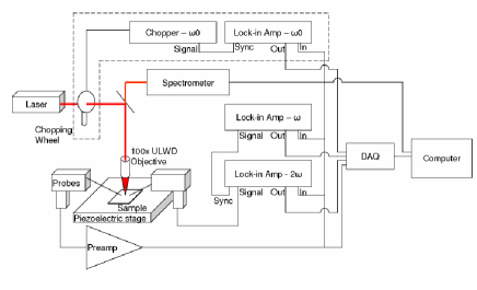
Using the measurement scheme shown in Figure 6 we measure the first and second harmonics of the low-frequency current using a lock-in amplifier, as well as the dc current. In the absence of any optical effect, (7) implies that the rectified current due to the low-frequency drive will be exactly equal to the lock-in current measured at the second harmonic of the source frequency, as we observe. Under illumination, plots of the dc current vs. the measured low-frequency ac current at for fixed input amplitude of 100 mV show that the dc current can exceed the low frequency dc contribution by nearly a factor of two. This implies a second source of dc current that scales linearly with and vanishes when the illumination is blocked.
To determine the particular optical mechanism at work, we measured the dependence of the dc current on optical power. We chop the incoming laser and measure the current component at the chopping frequency as shown in the Figure 6. Figure 7 shows a power curve measured at a few intensities, showing that the optically induced dc current depends linearly on the incident intensity, consistent with the optical rectification mechanism.
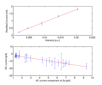
Assuming that optical rectification is at work we can estimate the enhancement of the electric field in the nanogap, as described above. By comparing the measured dc current to the low frequency ac current component at 2 at constant laser power we can determine how much of the rectified current is a result of optical rectification. Figure 7B shows a representative curve. The dc current is well fit by a line of slope -1.91. A slope of would have indicated that all the dc current is due to rectification of the applied low frequency signal. The sign of the slope varies from device to device depending on the sign of and thus the direction of the rectified current. It should be noted that both the low frequency and optical frequency parts should be rectified in the same direction. A slope of -1.91 indicates that . For this particular measurement =100 mV yielding =95 mV. Assuming a gap separation of 1 nm we can get the approximate optical field strength across the gap is V/m. The incident unenhanced optical field is V/m, yielding a field enhancement of approximately 500, and a total Raman enhancement of roughly , consistent with the predications for the necessary enhancement to observe single molecule SERS.
Unfortunately at room temperature and under higher intensity laser powers the nanogap stability is poor, making it difficult to perform a more in-depth analysis. Currently we do not have the capability to perform low temperature optical measurements; however, it is possible to examine these same rectification mechanisms at radio frequencies in a low temperature probe station. Optical rectification has been successfully demonstrated at microwave frequencies in STM measurements[69]. A measurement scheme analogous to that present in Figure 6 was used, with found by a low frequency measurement and the RF contribution to the rectified current measured by chopping the incident RF.
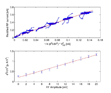
Devices were prepared by assembling pMA on the Au surface prior to the experiment. Measurements were made at 80 K in a vacuum probe station after electromigration. A 20 mV RMS low frequency sine wave was sourced by one lock-in amplifier and fed into a bias tee along with a 0-20 mV RMS RF signal. The RF signal was amplitude modulated from 0 to 100% a frequency (typically 157 Hz). The combined signal was sent into one electrode of the nanogap. The current flow through the device was measured at the other electrode using a current amplifier with 100 kHz low pass filter enabled to remove any RF component from the measured current. The output of the current amplifier was measured using three lock-in amplifiers measuring at , , and (lock-in source frequency, second harmonic, and RF chopping frequency) and the dc current was measured directly at the amplifier. A representative power curve plotting versus is plotted in figure 8 for an RF frequency of 10 MHz. A clear linear dependence is observed. The sloped of 4.48 is a result of an impedance mismatch between the RF function generator and the nanogap device. After accounting for this mismatch the slope is approximately 1 as expected for the rectification mechanism. From this series of measurements we infer that is frequency independent up to 1 GHz. A priori this does not imply that is frequency independent up to optical frequencies, though the results seen in figure 7 are consistent with this rectification mechanism beyond Hz.
5 Conclusions and prospects
Electromigrated gaps have proven to be an enormously useful tool in probing electronic properties in single molecules, though the lack of imaging techniques has meant that great care must be exercised in interpreting transport data. Pure electronic transport can contain signatures that are distinct to the molecules being probed (charging energies, vibrational resonances, Kondo physics). The recent observation that electromigrated junctions are highly effective optical antennas has great potential. Simultaneous measurements of transport and Raman spectra in single molecules are now possible, allowing the vibrational fingerprinting of the active electronic element in the junction. Detailed information about molecular orientation and bonding within the junction may be inferrable from the Raman data. Optical measurements also bring additional electronic transport mechanisms into play, as optical rectification measurements demonstrate. The promise of combined single-molecule electronic and optical characterization suggests that electromigrated molecular junctions have a bright future as tools for physics and physical chemistry at the molecular scale.
References
- [1] Ahn C H, Bhattacharya A, Di Ventra M, Eckstein J N, Frisbie C D, Gershenson M E, Goldman A M, Inoue I H, Mannhart J, Millis A J, Morpurgo A F, Natelson D and Triscone J-M 2006 Rev. Mod. Phys. 78 1185
- [2] van Ruitenbeek J, Alvarex A, Piñeyro I, Grahmann C, Joyez P, Devoret M, Esteve D and Urbina C 2002 Rev. Sci. Instrum. 89 086802
- [3] Datta S, Tian W, Hong S, Reifenberger R, Henderson J I and Kubiak C P 1997 Phys. Rev. Lett. 79 2530
- [4] Reed M, Zhou C, Muller C, Burgin T and Tour J 1997 Science 278 252
- [5] Scheer E, Agraït N, Cuevas J C, Yeyati A L, Ludolph B, Martin-Rodero A, Bollinger G R, van Ruitenbeek J M and Urbina C 1998 Nature 394 154
- [6] Stipe B, Rezaei M and Ho W 1998 Science 280 1732
- [7] Chen J, Reed M A, Rawlett A M and Tour J M 1999 Science 286 1550
- [8] Collier C, Wong E, Belohradsky M, Raymo F, Stoddart J, Keukes P, Williams R and Heath J 1999 Science 285 391
- [9] Donhauser Z J, Mantooth B A, Kelly K F, Bumm L A, Monnell J D, Stapleton J J, Price D W Jr, Rawlett A M, Allara D K, Tour J M and Weiss P S 2001 Science 292 2303
- [10] Wold D and Frisbie C 2001 J. Am. Chem. Soc. 123 5549
- [11] Cui X D, Primak A, Zarate X, Tomfohr J, Sankey O F, Moore A L, Moore T A, Gust D, Harris G and Lindsay S M 2001 Science 294 571
- [12] Reichert J, Ochs R, Beckmann D, Weber H, Mayor M and von Lohneysen H 2002 Phys. Rev. Lett. 88 176804
- [13] Smit R, Noat Y, Untiedt C, Lang N, van Hemert M and van Ruitenbeek J 2002 Nature 419 906
- [14] Kushmerick J, Holt D, Yang J, Naciri J, Moore M and Shashidar R 2002 Phys. Rev. Lett. 67 108
- [15] Ramachandran G, Hopson T, Rawlett A, Nagahara L, Primak A and Lindsay S 2003 Science 300 1413
- [16] Xu B Q and Tao N J 2003 Science 301 1221
- [17] Xiao X Y, Xu B Q and Tao N J 2004 Nano Lett. 4 267
- [18] Tao N J 2006 Nature Nano. 1 173
- [19] Venkataraman L, Klare J E, Tam I W, Nuckolls C, Hybertsen M S and Steigerwald M L 2006 Nano Lett. 6 458
- [20] Venkataraman L, Park Y S, Whalley A C, Nuckolls C, Hybertsen M S and Steigerwald M L 2007 Nano Lett. 7 502
- [21] Park H, Lim A K L, Alivisatos A P, Park J and McEuen P L 1994 Appl. Phys. Lett. 75 301
- [22] Bolotin K I, Kuemmeth F, Pasupathy A N and Ralph D C 2004 Appl. Phys. Lett. 84 3154
- [23] Park H, Park J, Lim A K L, Anderson E H, Allvisatos and McEuen P L 2000 Nature 407 58
- [24] Park J, Pasupathy A N, Goldsmith J I, Chang C, Yaish Y, Petta J R, Rinkoski M, Setna J P, Abrũna H D, McEuen P L and Ralph D C 2002 Nature 417 722
- [25] Liang W, Shores M P, Bockrath M, Long J R and Park H 2002 Nature 417 725
- [26] Yu L H and Natelson D 2004 Nano Lett. 4 79
- [27] Pasupathy A N, Bialczak R C, Martinek J, Grose J E, Donev L A K, McEuen P L and Ralph D C 2004 Science 306 86
- [28] Yu L H, Keane Z K, Ciszek J W, Cheng L, Stewart M P, Tour J M and Natelson D 2004 Phys. Rev. Lett. 93 266802
- [29] Pasupathy A W, Park J, Chang C, Soldatov A V, Lebedkin S, Bialczak R C, Grose J E, Donev L A K, Sethna J P, Ralph D C and McEuen P L 2005 Nano Lett. 5 203
- [30] Champagne A R, Pasupathy A N and Ralph D C 2005 Nano Lett. 5 305
- [31] Yu L H, Keane Z K, Ciszek J W, Cheng L, Tour J M, Baruah T, Pederson M R and Natelson D 2005 Phys. Rev. Lett. 95 256803
- [32] Heersche H B, de Groot Z, Folk J A, van der Zant H S J, Romeike C and Wegewijs M R 2006 Phys. Rev. Lett. 96 206801
- [33] Chae D-H, Berry, J F, Jung, S, Cotton, F A, Murillo, C A and Yao Z 2006 Nano Lett. 6 165
- [34] Danilov A V, Kubatkin S E, Kafanov S G, Flensberg K and Bj/ornholm T 2006 Nano Lett. 6 2184
- [35] van der Zant H S J, Kervennic Y V, Poot M, O’Neill K, de Groot Z, Thijssen J M, Heersche H B, Stuhr-Hansen N, Bjornholm T, Vanmaekelbergh D, van Walree C A and Jenneskens L W 2006 Faraday Disc. 131 347
- [36] Scott G D, Chickak K S, Peters A J, Cantrill S J, Stoddart J F and Jiang H W 2006 Phys. Rev. B 74 113404
- [37] Natelson D, Yu L H, Ciszek J W, Keane Z K and Tour J M 2006 Chem. Phys. 324 267
- [38] Osorio E A, O’Neill K, Wegewijs M, Stuhr-Hansen N, Paaske J, Bj/ornholm T and van der Zant HSJ 2007 Nano Lett. 7 3336
- [39] Danilov, A, Kubatkin, S, Kafanov, S, Hedegard, P, Stuhr-Hansen, N, Moth-Poulsen, K and Bj/ornholm, T 2008 Nano Lett. 8 1
- [40] Heersche H B, de Groot Z, Folk J A, Kouwenhoven, L P, van der Zant H S J, Houck, A A, Labaziewicz, J and Chuang, I L 2006 Phys. Rev. Lett. 96 017205
- [41] Strachan D R, Smith D E, Johnston D E, Park T H, Therien M J, Bonnel D A and Johnson A T 2005 Appl. Phys. Lett. 86 043109
- [42] Trouwborst M L, van der Molen S J and van Wees B J 2006 Appl. Phys. Lett. 99 114316
- [43] Strachan D R, Smith D E, Johnston D E, Guiton B S, Drndic M, Bonnel D A and Johnson A T 2006 Nano Lett. 6 441
- [44] Dong J and Parviz B A Nanotech. 17 5124
- [45] Taychatanapat T, Bolotin K I, Kuemmeth, F and Ralph D C 2007 Nano Lett. 7 652
- [46] O’Neill K, Osorio E A and van der Zant H S J 2007 Appl. Phys. Lett. 90 133109
- [47] Houck A A, Labaziewicz J, Chan E K, Folk J A and Chuang I L 2005 Nano Lett. 5 1685
- [48] Wu Z M, Steinacher M, Huber R, Calame M, van der Molen S J and Schönenberger 2007 Appl. Phys. Lett. 91 053118
- [49] Wolf E L, Principles of Electron Tunneling Spectroscopy 1985 Oxford University Press
- [50] Ferry D K and Goodnick S M 1997 Transport in Nanostructures Cambidge University Press
- [51] Perrine T M and Dunietz B D 2007 Phys. Rev. Lett. 75 195319
- [52] Ghosh A W, Zahid F, Datta S and Birge R R Chem. Phys. 281 225
- [53] De Franceschi S, Sasaki S, Elzerman J M, van der Wiel W G, Tarucha S and Kouwenhoven L P 2001 Phys. Rev. Lett. 86 878
- [54] Sukhorukov E V, Burkand G and Loss D 2001 Phys. Rev. B 63 125315
- [55] Heid R, Pintschovius L and Godard J M 1997 Phys. Rev. B 56 5925
- [56] Goldhaber-Gordon D, Shtrikman, Mahalu D, Abusch-Magder D, Meirav U and Kastner M A 1998 Nature 391 156
- [57] Cronenwett S M, Oosterkamp T H and Kouwenhoven L P 1998 Science 281 540
- [58] Jeong H, Chang A M and Melloch M R 2001 Science 293 2221
- [59] Kouwenhoven L P and Glazma L Physics World 33 2001
- [60] Wingreen N S and Meir Y 1994 Phys. Rev. B 49 11040
- [61] Parks J J, Champagne A R, Hutchison G R, Flores-Torres S, Abruña H D and Ralph D C, 2007 Phys. Rev. Lett. 99 026601
- [62] Ward D R, Grady N K, Levin C S, Halas N J, Wu Y, Nordlander P and Natelson D 2007 Nano Lett. 7 1396
- [63] Ward D R, Halas N J, Ciszek J W, Tour J M, Wu Y, Nordlander P and Natelson D 2008 Nano Lett. 10.1021/nl073346h, in press
- [64] Galperin M and Nitzan A, Phys. Rev. Lett. 2005 95 206802
- [65] Galperin M and Nitzan A, J. Chem. Phys. 2006 124 234709
- [66] Viljas J K, Pauly F and Cuevas J C, Phys. Rev. B 2007 76 033403
- [67] Wu S W, Ogawa N and Ho W, Science 2006 312 1362
- [68] Cutler P H, Feuchtwang T E, Tsong T T, Nguyen H and Lucas A A 1987 Phys. Rev. B 35 7774
- [69] Tu X, Lee J and Ho W 2006 J. Chem. Phys. 124 113110