Microwave Dielectric Loss at Single Photon Energies and milliKelvin Temperatures
Abstract
The microwave performance of amorphous dielectric materials at very low temperatures and very low excitation strengths displays significant excess loss. Here, we present the loss tangents of some common amorphous and crystalline dielectrics, measured at low temperatures ( 100 mK) with near single-photon excitation energies, , using both coplanar waveguide (CPW) and lumped resonators. The loss can be understood using a two-level state (TLS) defect model. A circuit analysis of the half-wavelength resonators we used is outlined, and the energy dissipation of such a resonator on a multilayered dielectric substrate is considered theoretically.
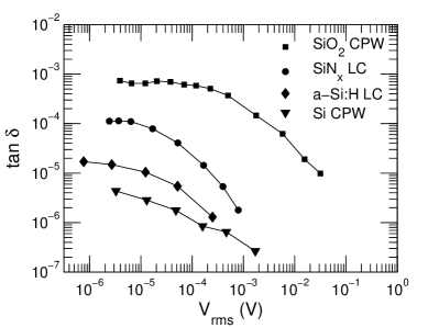
Dielectric loss is a significant concern for superconducting quantum bits (qubits), as energy relaxation within the dielectric is one of the primary sources of quantum decoherenceMartinis:2005 . Superconducting qubits operate in the low-temperature, low-voltage regime, where dielectric loss is typically not well characterized. While the dielectric loss may be extremely small at higher excitation voltages and temperatures, it has been observed that the loss tangent scales inversely with voltage () and levels off at an intrinsic value that is often substantially greater than the loss at larger voltages, as shown in Fig. 1. The lowest excitation voltages shown there correspond to of order 1 photon in a 6 GHz resonator, with pF.

This behavior has been postulated to arise from coupling to a bath of TLS defects in the dielectric, which absorb and disperse energy at low power but become saturated with increasing voltage and temperature Shnirman:2005 . TLS are found in most amorphous materials and arise from an energy difference between defect bond configurations coupled by tunneling. The bath of TLS is assumed to have a constant distribution in energy and a log uniform distribution in transition strength Hunklinger:1986 . These defect states couple to the surrounding electric field through the electric dipole moments that arise from differences in the charge distribution between configurations Schickfus:1977 .
Although dielectric loss at higher powers and temperatures has been extensively reported, the literature contains very little information on dielectric performance in the low-temperature, low-voltage limit. Guided by prior measurements of hydrogenated dielectrics with over-constrained lattices Pohl:2002 , we examined the microwave loss of a range of dielectric materials compatible with qubit fabrication. Here we report direct measurements of the intrinsic loss tangents of these dielectric materials.
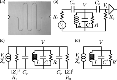
To perform these measurements, we fabricated both parallel resonators, comprising a superconducting inductive coil and a parallel-plate capacitor containing the dielectric in question, and half-wavelength CPW resonators, where the single-layer superconducting metal electrodes are patterned atop the dielectric. A CPW resonator is shown in Fig. 2(a). resonators afford more straightforward analysis of the loss tangent, due to the parallel electric field configuration between the plates, while CPW resonators are easier to fabricate, but require more complicated analysis. Both types of resonators were coupled to measurement lines through on-chip coupling capacitors , as illustrated in Fig. 2(b). The resonators had resonance frequencies near the 6 GHz operating frequencies of our qubits. The resonators’ transmission -parameter, , was measured as a function of voltage and temperature, using a vector network analyzer. The loss tangents were extracted as described below. The results of these measurements are compiled in Table I.
| Dielectric | Metal | Resonator | |
|---|---|---|---|
| 100 -cm Si (SC) | Al | CPW | 512 |
| Sapphire (SC) | Re | CPW | 610 |
| Sapphire (SC) | Al | CPW | 921 |
| -Si:H | Al | 2225 | |
| -Si:H | Al | CPW | 10130 |
| Interdigitated cap. | Al | 4147 | |
| on sapphire (SC) | |||
| SiNx | Re or Al | or CPW | 100200 |
| Thermal SiO2 | Al | CPW | 300330 |
| Sputtered Si | Al | CPW | 500600 |
| AlN | Al | CPW | 11001800 |
| PECVD SiO2 | Al | CPW | 27002900 |
| MgO | Al | CPW | 50008000 |
Near its half-wave resonance frequency, a CPW resonator can be represented by an equivalent lumped circuit, shown in Fig. 2(b). The Norton equivalent circuit is shown in Fig. 2(c), where the voltage source has been transformed to a current bias , and the impedance can be written as , where we have used for typical coupling capacitances on the order of a few fF. This can now be viewed as a parallel circuit with effective capacitance and resistance (Fig. 2(d)). The response at frequency , near the resonance frequency , is given by
| (1) |
The output voltage , as shown in Fig. 2(b), is given by . The normalized scattering matrix parameter is given by , where we have used for the on-resonance transmittance of a lossless resonator. Finally, taking , , and assuming , we obtain
| (2) |
This equation is used to fit our measured data, from which we can extract the total measured quality factor . The quality factor is attributed to the parallel sum of two independent loss mechanisms, , where is the internal dielectric loss, and the loss due to the measurement impedance . We calculate either from the formula , where is the resonator characteristic impedance, or through the relation for over-coupled samples, when saturates at high powers and . Finally, the limiting loss tangent is related to at the lowest excitation voltage, .
For an resonator, this limiting loss tangent is a direct measurement of the low-power, low-temperature intrinsic loss of the dielectric, . This can be seen by noting that the electric field in an resonator is almost entirely confined to the space between the capacitor plates. Furthermore, the inductive loss is typically negligible at these temperaturesMazin:2002 . However, in a CPW resonator, the electric field samples a large volume of space around the CPW not filled by the dielectric of interest, so the limiting loss tangent is not identical to the intrinsic loss tangent. For a CPW resonator fabricated on a multi-layer substrate, it is necessary to know the fraction of the electrical energy stored in each dielectric, and the intrinsic loss tangents for all but one of the constituent dielectrics, as well as the value of limiting loss tangent for the composite structure.

This can be seen by considering the quality factor of a resonator driven at frequency , defined as , where and are the time-averaged magnetic and electric energies stored in a given volume, respectively, and is the time-averaged power dissipated in that volumePozar:2005 . For a resonator driven on resonance, and , so that . Furthermore, can be expressed as , where is the spatially-varying complex dielectric constant. Ignoring magnetic loss, which we do not believe to contribute significantly, this reduces to . With , we can re-express the resonant quality factor as
| (3) |
It is useful to consider the time-averaged electric energy divided by the quality factor,
| (4) |
This is a general expression for a spatially-varying dielectric constant. In our structures, the total volume can be divided into distinct isotropic regions.
For example, for a CPW resonator formed by Al patterned on 100 nm SiNx, on a 100 -cm single-crystal Si substrate, we separate Eq. (4) into two parts, , where the volumes and correspond to the regions occupied by the SiNx and the Si, respectively. This can be re-written as , or in terms of the intrinsic loss tangents and as
| (5) |
A finite-element analysis of the electric field distribution shows 11 of the total time-averaged energy is stored in the SiNx, 81 in the Si, and the remainder in vacuum. An independent measurement of the loss for SiNx, using an resonator, yielded . The intrinsic loss tangent for single-crystal silicon was extracted from the analysis of a CPW resonator on 100 -cm Si, yielding . Using Eq. 5, we calculate an expected loss tangent for the composite sample of . The measurement yielded , in excellent agreement.

Equation 4 can also be used to extract the intrinsic loss of a given dielectric layer, once the intrinsic loss tangents of the other layers in the structure are known. In this way we extracted the intrinsic loss tangents of all the dielectrics measured with CPW resonators, as tabulated in Table I. For example, a sample of Al/300nm SiO2/100 -cm Si was used to measure the loss of thermal SiO2 that was commercially grown in a furnace. The limiting loss tangent of this CPW resonator was ; a finite-element analysis showed that 27 of energy is stored in the SiO2, 61 in the Si, and 12 in the vacuum. We thus find that the intrinsic loss tangent of thermal SiO2 is .
As expected, thermal SiO2 exhibits comparatively high lossLiu:1997 . The results of Table I imply that a more highly constrained lattice is correlated to lower loss. This can be seen in the silicon compounds where the transition from SiO2 SiNx a-Si:H single-crystal Si corresponds to an increase in coordination number and a decrease in loss. Furthermore, the lower bounds on single-crystal Si and sapphire are not known precisely, because the measurements may be limited by factors other than dielectric loss, such as radiation. However, fabricating devices with single-crystal dielectrics is more difficult than using easily deposited amorphous materials. Due to this, we are currently optimizing the deposition of a-Si:H since it is the least lossy amorphous material, and in general, the loss tangent has been seen to correlate to the coherence times in our phase qubitsNeeley:2008 .
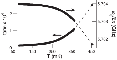
These measurements were all taken at temperatures near 100 mK. At higher temperatures the dielectric loss may be overshadowed by the loss in the superconducting Al electrodes Mattis:1958 . In Fig. 3 we display the temperature-dependent loss of an Al/100 -cm Si CPW. The higher loss with increasing temperature, and the frequency shift, are consistent with other measurements Mazin:2002 ; Mazin:2006 .
In conclusion, we have reported the low voltage, low temperature, intrinsic loss of many dielectrics. Furthermore, we have shown how to extract the intrinsic dielectric loss from CPW resonator data and find the results of measured CPW resonators to be commensurate with values given by LC resonators. Discovering other materials with lower loss tangents than the dielectrics reported here would offer significant improvements in qubit coherence times, and may be a crucial step in developing a scalable superconducting quantum computer.
Acknowledgements. Devices were made at the UCSB and Cornell Nanofabrication Facilities, a part of the NSF-funded National Nanotechnology Infrastructure Network. This work was supported by ARDA under grant W911NF-04-1-0204 and by the NSF under grant CCF-0507227.
References
- (1) J. M. Martinis, K. B. Cooper, R. McDermott, M. Steffen, M. Ansmann, K. D. Osborn, K. Cicak, S. Oh, D. P. Pappas, R. W. Simmonds and C. C. Yu, Phys. Rev. Lett. 95, 210503 (2005).
- (2) A. Shnirman, G. Schon, I. Martin and Y. Makhlin, Phys. Rev. Lett. 94, 127002 (2005).
- (3) S. Hunklinger and A. K. Raychaudhuri, Prog. Low Temp. Phys. 9, 265 (1986); Amorphous Solids: Low-Temperature Properties, ed. W. A. Phillips (Springer, Berlin, 1981).
- (4) M. v. Schickfus and S. Hunklinger, Phys. Lett. A 64, 144 (1977).
- (5) R. O. Pohl, X. Liu and E. J. Thompson, Rev. Mod. Phys. 74, 991 (2002).
- (6) B. A. Mazin, P. K. Day, H.G. LeDuc, A. Vayonakis and J. Zmuidzinas, Proc. SPIE, 4849, 283 (2002).
- (7) David M. Pozar, Microwave Engineering (John Wiley & Sons, Inc., New York, 2005).
- (8) X. Liu, B. E. White, Jr., R. O. Pohl, E. Iwanizcko, K. M. Jones, A. H. Mahan, B. N. Nelson, R. S. Crandall and S. Veprek, Phys. Rev. Lett. 78, 4418 (1997).
- (9) M. Neeley, M. Ansmann, R. C. Bialczak, M. Hofheinz, N. Katz, E. Lucero, A. O’Connell, H. Wang, A. N. Cleland and J. M. Martinis, submitted.
- (10) D. C. Mattis and J. Bardeen, Phys. Rev. 111, 412 (1958).
- (11) B. A. Mazin, M. E. Eckart, S. Golwala, B. Bumble, P. K. Day, J. Zmuidzinas and F. A. Harrison, Appl. Phys. Lett. 89, 222507 (2006).