Robust strongly-modulated transmission of a -shaped structure with local Rashba interaction
Abstract
We propose a scheme of spin transistor using a -shaped structure with local Rashba interaction. A wide antiresonance energy gap appears due to the interplay of two types of interference, the Fano-Rashba interference and the structure interference. A large current from the gap area can be obtained via changing the Rashba strength and/or the length of the sidearm by using gate voltage. The robustness of the antiresonance gap against strong disorder is demonstrated and shows the feasibility of this structure for the real application.
pacs:
85.75.-d, 73.23.Ad, 72.25.-bSpin-polarized electron transport has attracted much attention recently due to the promising application of spintronic devices.spintronics One of such devices, the Datta-Das spin field effect transistor,datta was proposed by utilizing the spin precession due to the Rashba effective magnetic field.rashba After that, the role of the Rashba spin-orbit coupling (SOC) in ballistic transport systems has been extensively studied.sato Very recently, the effect of local Rashba spin-orbit interaction in quasi-one dimensional quantum wires was investigated.sanchez2 As reported, there exists at least one bound state localized in the vicinity of the Rashba region due to the equivalent attractive potential from local Rashba interaction. Such bound state can interfere with direct propagating channels, leading to the Fano asymmetric lineshapesfano ; chu ; nockel of the transmission.sanchez2 Therefore, this effect was called the Fano-Rashba effect. Similar Fano-type inference effect in the quantum wire with an applied magnetic field was also reported, which was based on the interplay of the transmission channel with certain spin and the evanescent mode with opposite spin.sanchez The transmission zero dip at Fano antiresonance was proposed to be helpful in realizing spin transistor by Sanchez et al. very recently.sanchez However, the robustness of this proposal against the disorder, which is essential for real application, remains questionable. In this report, we will show that the occurrence of such dip is strongly limited by the disorder. We further propose a scheme of device using -shaped structuresols ; feng with local Rashba interaction. This device can provide a large energy window for antiresonance in contrast to single energy points in the ordinary antiresonance devises, with strong robustness against disorder.
A schematic of the waveguide in our study is shown in Fig. 1, where a waveguide of length with a sidearm protruding from the center, is connected to the half-metallic leads through perfect ideal ohmic contacts. We assume the electron states at the Fermi level are all spin-down ones in the leads, so that only spin-down electrons can propagate into/out of the -shaped structure. The effective length of the sidearm can be adjusted electronically by a gate voltage .feng The finite width of the waveguide gives the propagation threshold as the first quantized subband along the transversal direction. A perpendicular magnetic field is applied uniformly on the whole device. This field shifts the energy spectrum by a Zeeman splitting . We neglect the effect of magnetic field on orbital motion by assuming the magnetic field is weak and hence the Landau level is negligible. The interference of the different Feynman paths makes it possible to realize spin transistor using -shaped structure.sols However, this kind of transistor is also strongly limited by the disorder as we will show later. In order to get a robust transistor, we further introduce the local Rashba interaction as the gray area in Fig. 1. From Fano-type interference effect due to the local Rashba interaction, the transmission of the propagating channel can also be strongly modulated, especially at the Fano antiresonance.sanchez ; sanchez2 We demonstrate that when the individual structure antiresonance and Fano antiresonance are close to each other, there exists a broad energy window in which the conductance is zero, i.e., there exists an antiresonance energy gap. This is in contrast to the single (specific) energy when only the structure or Fano antiresonance is involved. Moreover, this antiresonance energy gap is very robust against the disorder. We also find that a large current can be obtained in this gap area by adjusting the Rashba coupling strengthnitta and/or the length of the sidearm using the gate voltage. Such features are very useful for the spin transistors.

We describe the -shaped structure by the tight-banding Hamiltonian with the nearest-neighbor approximation
| (1) | |||||
with two indices and denoting the site coordinates along the and axes, respectively. The lattice energy , with the hopping energy and the Zeeman splitting . Here and stand for the effective mass and lattice constant separately. The last term in Eq. (1) describes the Rashba SOCrashba ; mireles
| (2) | |||||
in which with representing the Rashba coefficient. The summations in are performed only in the gray area in Fig. 1.

The two-terminal conductance is obtained from the Landauer-Büttiker formulalandauer
| (3) |
where denotes the self-energy of the isolated ideal leads and () is the retarded (advanced) Green function.datta2 For energy window , the current is given by . We perform a numerical calculation for a waveguide with fixed width . The hard wall potential in the transverse direction gives the lowest energy of the th subband . Throughout this report, we take the Zeeman splitting energy and the Fermi energy is regard to . The conductance represents the conductance of the only propagating spinor .
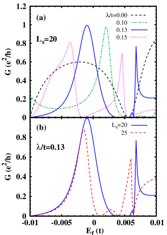
In Fig. 2(a), the conductance is plotted as a function of the Fermi energy at different Rashba coefficients . In the calculation, . The result without the local Rashba SOC is plotted as the black dashed curve, showing a transmission zero dip, i.e., the structure antiresonancefeng ; shi dip, at . The presence of the local Rashba interaction also strongly influences the conductance and provides another transmission zero dip, i.e., the Fano antiresonance dip, as shown by the remaining curves with . One finds that the Fano dip moves to small region with the increase of the SOC coefficient.sanchez The most interesting feature is that when the Fano dip is close to the structure dip (), a wide energy gap [0.0034t,0.0058t] for antiresonance appears (see the blue solid curve). Moreover, this gap can be turned off via changing the SOC coefficient. Specifically, there exists a peak at , which gives a current for the energy window , originally in the gap area. Therefore, it can work as spin transistor with the on and off features by tuning the Rashba strength with a gate voltage. From Fig. 2(b), one can also see that the on and off features of the transistor can also be remotely controlled by changing the length of the sidearm by another gate voltage.feng


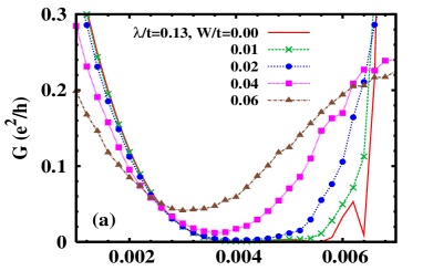
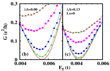
We now show the feasibility of the above proposed device for real application by analyzing the robustness of the antiresonance gap [i.e., the solid blue curve in Fig. 2(a)] against the Anderson disorder. The converged conductance which is averaged over 3000 random configurations is plotted in Fig. 3(a) against the Fermi energy in the vicinity of the gap for different Anderson disorder strength . From the figure, one can see that the leakage conductance near the gap is extremely small () until the strength of the disorder exceeds which is three times larger than the Zeeman splitting. For the large disorder strength , the corresponding leakage current for the energy window is smaller than , more than one order of magnitude smaller than the “on” current in the same energy interval. The leakage current is even much smaller for (), i.e., (). For comparison, we also check the robustness of the previous proposed transistors.feng ; sanchez In Fig. 3(b), the results of -shaped structure without the local Rashba SOC are plotted. The conductance increases rapidly with the strength of the disorder, specifically, it reaches already at . Similar feature is also obtained for the device with only the Fano antiresonance where the length of the side arm and , as shown in Fig. 3(c). Therefore, the transistors based on the structure antiresonance or the Fano antiresonance alone are very weak against the disorder and do not provide an energy window, both in contrast to our new scheme which combine both the Fano and the structure antiresonance together. We also checked the robustness of the antiresonance gap against the disorder of the Rashba SOC, and obtained results very similar to the case with the on-site disorder. The average leakage conductance in the gap is about with a disorder strength , which is much smaller than the conductance with the same disorder strength at the Fano-antiresonance point in structure without sidearm ().
In summary, we have proposed a scheme for spin transistor by studying a -shaped structure with local Rashba SOC. Both leads are assumed to be half-metallic. The relevant conductance can be strongly modulated by the Fermi energy of the leads, the strength of the Rashba SOC and the length of the sidearm. We have also demonstrated that a wide antiresonance energy gap can be obtained by adjusting the Fano antiresonance and the structure antiresonance close to each other. We propose that our structure can be used as spin transistors, since a large current can be obtained in the same antiresonance energy gap region when the two types of the antiresonance are tuned away from each other by either change the Rashba coefficient and/or change the length of the side arm electronically. We also show the robustness of the antiresonance energy gap against the on-site disorder. The wide working energy window (in contrast to a single energy) and the much improved robustness against disorder suggest the proposed structure has great potential for real application.
This work was supported by the Natural Science Foundation of China under Grant Nos. 10574120 and 10725417, the National Basic Research Program of China under Grant No. 2006CB922005 and the Knowledge Innovation Project of Chinese Academy of Sciences. One of the authors (MWW) was also partially supported by the Robert-Bosch Stiftung and GRK 638. He would like to thank J. Fabian and C. Schüller at Universität Regensburg for hospitality where this work was finalized and J. Fabian for valuable discussions. S.K. acknowledges J. Zhou for valuable discussions.
References
- (1) Semiconductor Spintronics and Quantum Computation, edited by D. D. Awschalom, D. Loss and N. Samarth (Springer-Verlag, Berlin, 2002); I. Z̆utić, J. Fabian, and S. Das Sarma, Rev. Mod. Phys. 76, 323 (2004); J. Fabian, A. Matos-Abiague, C. Ertler, P. Stano, and I. Zutić, acta physica slovaca 57, 565 (2007); and references therein.
- (2) S. Datta and B. Das, Appl. Phys. Lett. 56,665 (1990).
- (3) E. I. Rashba, Fiz. Tverd. Tela (Leningrad) 2, 1224 (1960).
- (4) Y. Sato, S. Gozu. T. Kikutani, and S. Yamada, Physica B 272, 114 (1999); A. V. Moroz and C. H. W. Barnes, Phys. Rev. B 60, 14272 (1999); A. A. Kiselev and K. W. Kim, Appl. Phys. Lett. 78, 775 (2001); S. Bellucci and P. Onorato, Phys. Rev. B 68, 245322 (2003); V. Marigliano Ramaglia, V. Cataudella, G. De Filippis, and C.A. Perroni, Phys. Rev. B 73, 155328 (2006); F. Zhai and H. Q. Xu, Phys. Rev. Lett. 94, 246601 (2005); C.A. Perroni, D. Bercioux, V. Marigliano Ramaglia, and V. Cataudella, J. Phys.: Condens. Matter 19, 186227 (2007).
- (5) D. Sánchez and Ll. Serra, Phys. Rev. B 74, 153313 (2006).
- (6) C. S. Chu and R. S. Sorbello, Phys. Rev. B 40, 5941 (1989).
- (7) J. U. Nöckel and A. D. Stone, Phys. Rev. B 50, 17415 (1994).
- (8) U. Fano, Phys. Rev. 124, 1866 (1961).
- (9) D. Sánchez, Ll. Serra, and M. Choi, Phys. Rev. B 77, 035315 (2008).
- (10) F. Sols, M. Macucci, U. Ravaioli, and K. Hess, J. Appl. Phys. 66, 3892 (1989).
- (11) X. F. Feng, J. H. Jiang, and M. Q. Weng, Appl. Phys. Lett. 90, 142503 (2007).
- (12) J. Nitta, T. Akazaki, H. Takayanagi, and T. Enoki, Phys. Rev. Lett. 78, 1335 (1997).
- (13) F. Mireles and G. Kirczenow, Phys. Rev. B 64, 024426 (2001).
- (14) M. Büttiker, Phys. Rev. Lett. 57, 1761 (1986).
- (15) S. Datta, Electronic Transport is Mesoscopic Systems (Cambridge University Press, New York, 1995).
- (16) Q. W. Shi, J. Zhou, and M. W. Wu, Appl. Phys. Lett. 85, 2547 (2004).