The first version Buffered Large Analog Bandwidth (BLAB1) ASIC for high luminosity collider and extensive radio neutrino detectors
Abstract
Future detectors for high luminosity particle identification and ultra
high energy neutrino observation would benefit from a digitizer
capable of recording sensor signals with high analog bandwidth and
large record depth, in a cost-effective, compact and low-power way.
A first version of the Buffered Large Analog Bandwidth (BLAB1) ASIC
has been designed based upon the lessons learned from the development
of the Large Analog Bandwidth Recorder and Digitizer with Ordered
Readout (LABRADOR) ASIC. While this LABRADOR ASIC has been very
successful and forms the basis of a generation of new, large-scale
radio neutrino detectors, its limited sampling depth is a major
drawback. A prototype has been designed and fabricated with 64k deep
sampling at multi-GSa/s operation. We present test results and
directions for future evolution of this sampling technique.
keywords:
Super B factory, particle identification, CMOS, radio neutrino detectionPACS:
85.40.-e, 85.40.Qx, 87.66.Pm, , and
1 Introduction
Observation of the early universe through neutrino messengers of the highest possible energies requires a detector of enormous instrumented volume [1]. At the same time, lepton flavor identification of such radio detection events represents a completely unique tool for the study of cosmological evolution of the universe. Particle interactions at extreme energies provide a probe capable of illuminating the completely unknown acceleration mechanisms of the highest energy cosmic ray events [2].
Particle identification is also crucial to the physics program of a next generation “Super” B Factory. Such an accelerator will produce B mesons in sufficiently copious quantities to permit detailed scrutiny of standard model predictions in the flavor sector [3]. Any new theories for physics beyond the standard model must leave fingerprints that can be detected via flavor transformation of particles in the final state. Therefore, particle identification is essential and the detector and readout electronics must survive the very high signal occupancies expected [4].
We present results from a deep-sampling ASIC that meets these requirements, based upon extension of the successful LABRADOR ASIC [5].
2 Architectural Details
The BLAB1 ASIC is a single channel, multi-GSa/s waveform sampler with a record depth of analog storage samples. The BLAB1 analog input is AC coupled with an external capacitor and 50 terminated with an on-chip terminator, as should be expected for a high-performance RF device. After the on-chip terminator, an analog buffer tree fans out copies of the signal to the matrix of 128 rows of 512 samples composing the 64k array. Each of the rows may be independently addressed to initiate a storage cycle. Within each Switched Capacitor Array (SCA) storage cell is a capacitor and a comparator. A block diagram of the BLAB1 readout is shown in Fig. 1.
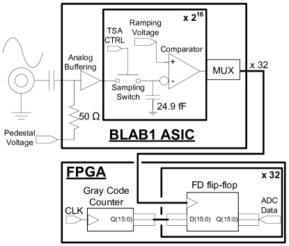
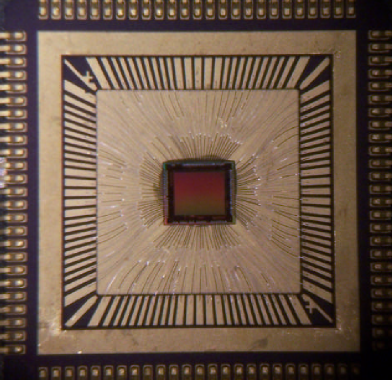
When an analog switch is pulsed closed, the instantaneous input signal is stored on a 14 fF capacitor. The charge is then held until either overwritten or discharged due to leakage current. Each sampling capacitor is connected to the negative input of a comparator. The positive input of each comparator is connected to a common voltage ramp. A wire-bonded BLAB1 die photograph is shown in Fig. 2, with this storage array contained within about 5.25 square mm of the die shown.
Conversion of these stored samples is via a Wilkinson ADC method, where the stored voltage is converted into a transition time of the in-cell comparator due to an applied voltage ramp. This ramp is generated with a current mirror and can be adjusted both by varying the ramping current, as well as an external capacitor. The typical ramping current range is 10-100A and the ramp capacitor size is a few hundred . Encoding is performed by measuring the time interval between the ramp start and the comparator output transition. In a simple form of time-to-digital conversion, this interval is measured by counting the number of high-speed clock cycles taken. In the predecessor ASIC [5], the Gray code counter was implemented on-chip, whereas in BLAB1 it is implemented inside a companion programmable logic device, in this case a Field Programmable Gate Array (FPGA). When the voltage ramp is started, a Gray code counter in the FPGA is enabled coincident to a high speed clock (500MHz) and the comparator output is used to latch the counter value. By knowing the ramping voltage slope and the high speed clock frequency, the latched counter value can be converted into voltage. A group of 32 comparators are selected, as illustrated in Fig. 3, and are read out during each ramping cycle.
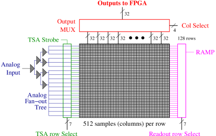
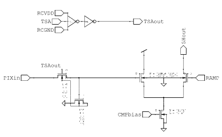
By addressing a row and selecting a group of 32 columns for each conversion cycle, the window of interest inside the ASIC is read out. Importantly, this readout operation can be done while sampling continues, providing continuous pipelining and subsequent deadtime reduction. This decision to move the high-speed clock and registers off-chip also means that the size of each storage cell can be significantly reduced. A schematic of the base BLAB1 storage cell is shown in Fig. 4, where the comparator is simply a differential NMOS pair. The corresponding layout is shown in Fig. 5, where the overall dimensions are by , where m. This corresponds to 4.8m by 16.68m, or about 80 required per storage cell.
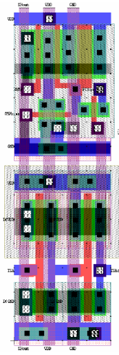
Therefore the core of the sampling array requires only 5.25 of chip area, permitting more than an order of magnitude improvement in storage density compared with existing devices [5, 6, 7, 8]. Reducing the cell size and subsequently the storage capacitance also helps improve the bandwidth that can be coupled into each storage cell. Since the “on” resistance of the switch is relatively high (), frequencies above
| (1) |
will roll off for a given pixel capacitance . The extracted capacitance value for the layout in Fig. 5 is approximately 14 fF. Therefore the expected from the common input bus line into each storage cell is approximately 2.3 GHz.
We note that the size of the storage cell can be reduced further by removing individual sample delay timing chains from each storage row. As seen in the bottom of Fig. 5, this inverter pair is more than half the area of the storage cell. For power dissipation reasons, this removal turns out to be important, as will be discussed later.
A further benefit of decoupling the latching register and clocking functionality is that the conversion clock can be run at a much higher speed inside the FPGA, since it is routinely fabricated in either a 65nm or 90nm process, compared with the relatively coarse 250nm (0.25m) process of BLAB1. Typically with the chosen Xilinx Virtex family employed we are able to use a 500MHz clock, and record the phase of the clock as well, thereby effectively having a 1ns least count. Separate testing indicates that this TDC performs very close to the ideal binary interpolation limit (ps), as reported previously [9]. Moreover, the number of bits of resolution or precision can be completely configurable, which permits a trade-off of the readout latency versus required sample resolution for various applications. We note in passing that there is a potentially much better method based upon applying this same waveform sampling technique to the timing encoding of the comparator output. The TDC least count would then become 1ns ps, and fitting the output shape, better than binary encoding time resolution may be possible.
While the coupling into individual storage cells can support high analog bandwidth (GHz), the cumulative capacitance seen when trying to drive the array of 64k cells is very problematic. The extracted capacitance of each of the switch drains is about 1.5fF, which sums to a total array capacitance of 98pF. Clearly, for a reasonably low input coupling impedance of , this bandwidth limitation to
| (2) |
would be completely unacceptable. Therefore a 3-level buffer tree has been employed, to reduce the loading seen at each stage of signal fan-out. The unity gain for zero capacitance of these buffer amplifiers is in excess of 1GHz. In retrospect, the choice of fanout: was not optimal, as the capacitance of the intermediate state was rather high and limits the performance, as will be shown in the testing section.
The sampling speed is controlled by adjusting the VDD/VSS supply voltages of one of the two inverter-inverter delay stages between each adjacent sampling cell in a particular sampling row.
As mentioned early, by addressing a row and pulsing the first cell of that particular row, a write strobe then propagates along the row until it reaches the last cell in the row. The leading edge of the pulse closes the switch and the trailing edge opens the switch, at which point the analog voltage value is stored.
Upon the determination of an external trigger condition, further sampling to the row(s) or interest are blocked in firmware and a ramping voltage is generated by using a constant current source and reference capacitor, as mentioned earlier. The ramping voltage for the BLAB1 can be generated using either an external capacitor or an on-chip capacitor. A external capacitor is necessary for slower ramping speeds. The current source is set by an external resistor. A unique feature of the BLAB1’s digitization technique is that the ADC resolution does not have a default value. For a fixed clock frequency, reducing the ramping voltage speed will increase ADC resolution. However, by using a slower ramp, it will take longer to digitize.
BLAB1 was designed to be a low power ADC. Three voltage sources are required to operate the BLAB1. A voltage source of 2.5 volts is the main power source. An adjustable VDD source is used to control the sampling speed. A pedestal voltage, typically 1.3 volts, is used to set the DC offset of the RF input. When in quiescent mode, the power draw can be 10mW or less. A list of the key BLAB1 specifications are summarized in Table 1.
| Item | Value |
|---|---|
| Sampling Input Channels | 1 |
| Storage rows | 128 |
| Storage cells/row | 512 |
| Total storage cells | 65,536 |
| Sampling speed (GSa/s) | 0.1 - 6.0 |
| Storage record | 10.9 - 655 s |
| Wilkinson Outputs | 32 |
| Operation mode | continuous storage/readout |
| 100ns window readout | 80s (5.12 GSa/s, 12-bits) |
| Full chip readout | 10ms (12-bits) |
3 Readout Test System
A series of printed circuit boards have been fabricated to evaluate various aspects of BLAB1 performance. Beyond this, these evaluation devices are proving useful for instrumenting a next generation of Cherenkov radiation detectors [10]. A photograph of a 2 BLAB1 ASIC (precision differential timing evalution) circuit board is shown in Fig. 6.
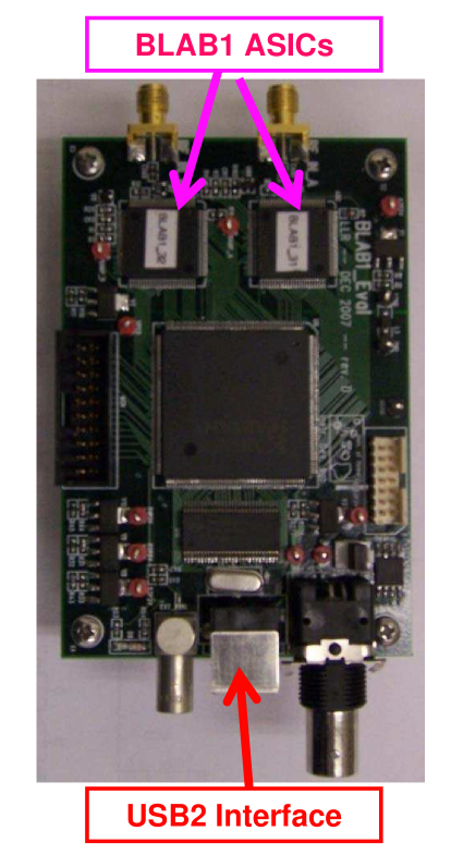
The three main components on this circuit board are two BLAB1 chips, an FPGA (largest package in center), and a Universal Serial Bus (USB) interface. The external communication protocol is USB 2.0. A USB microcontroller, the Cypress CY7C68013-56PVC, located on the circuit board interprets the USB 2.0 protocol and controls the flow of data being sent and received from the FPGA to a computer interface. The FPGA used is a Xilinx XC3S400 and controls the digital logic and timing for the BLAB1 readout. An internal FPGA RAM buffers the data while the data is being dumped into the USB data stream. A custom readout and control software utility was developed using the wxWidgets tool kit [11], a screen shot of which is shown in Fig. 7.
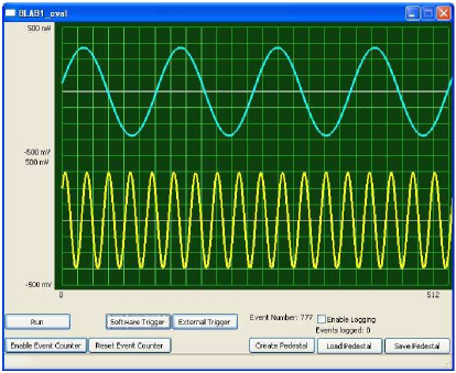
In this configuration, it becomes apparent that this BLAB1 “oscilloscope on a chip” can, with this small readout board, turn any PC (or laptop) into a high-performance digital signal oscilloscope. This software package sends commands to the FPGA and records the BLAB1 data via the USB 2.0 interface. Running this utility on a standard PC, a sustained triggered event rate of approximately 7kHz (single row readout) has been demonstrated. This rate should not be considered a hard limit as neither the software nor the firmware was optimized for speed. The sampling rate is controlled by setting a DAC, which then adjusts the VDD voltage (ROVDD) of the on-chip voltage-controlled delays.
4 Basic Sampler Performance
Employing the test system described in the previous section and its variants, a number of the basic performance parameters of the BLAB1 have been evaluated. Because timing performance is such a critical feature of this sampling device, it is described in detail in a subsequent section.
4.1 Sampling speed
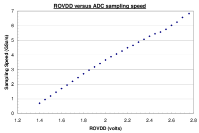
Determination of the sampling speed is made by measuring the time interval between insertion of the timing strobe and appearance of the output pulse from the last cell of the row, minus pad buffer delays. The sampling speed is calculated by taking the number of cells in a row and dividing it by the propagation time for a given control voltage setting. A plot of the sampling speed versus control voltage (ROVDD) is shown in Fig. 8, where it is seen that sampling rates from below 1.0 GSa/s to above 6.0 GSa/s are possible.
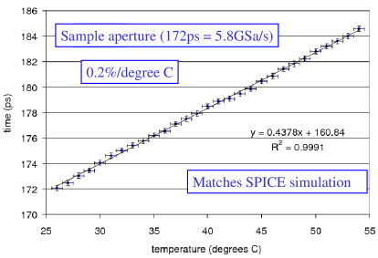
One potential disadvantage of this voltage controlled delay technique is that the circuit is temperature dependent. This dependence is seen in Fig. 9 and is roughly 0.2%/∘C, and completely matches expectation from SPICE simulation. While for many applications this variation would not be significant, and can potentially be calibrated out with an external reference clock [5], the delay can also be monitored and stabilized using a firmware control loop.
4.2 Noise performance
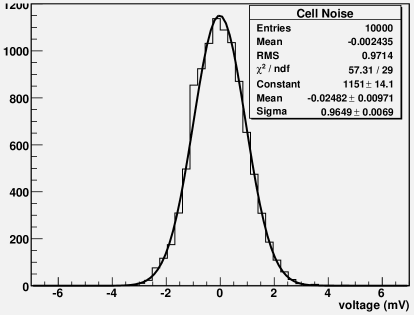
Noise distributions were measured for all storage cells in the process of determining the pedestal values. These measurements are made by terminating the BLAB1 analog input, and reading each cell multiple times. An example of the the noise distribution for a typical storage cell is shown in Fig. 10, which represents the ensemble mean noise average of about 1 mV RMS. With an input dynamic range of greater than 1 Volt (1.5V nom.) and this average noise level, each stored sample represents 10 real ADC bits of resolution, which is very competetive with commercially available, large power-dissipation ADCs [12].
For comparison, the expected RMS noise due to the small charge quantization
| (3) |
where is Boltzmann’s constant and we take to be 300K. Plugging in the from above, we expect a contribution due to this “kTC” noise of
| (4) |
which subtracted in quadrature indicates that the excess ASIC and board level noise is approximately 0.84mV, and could perhaps be improved through better layout.
4.3 Analog bandwidth
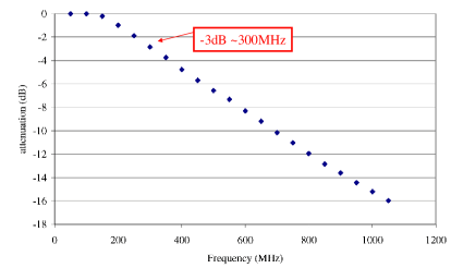
A determination of the analog frequency response of the BLAB1 ASIC was performed by recording fixed amplitude sine waves of varying frequencies and comparing the ratio of the actual amplitude to the recorded amplitude. The amplitude roll-off versus frequency is shown in Fig. 11, where the -3 dB attenuation point is about 300 MHz, and the -10dB point extends beyond 600 MHz.
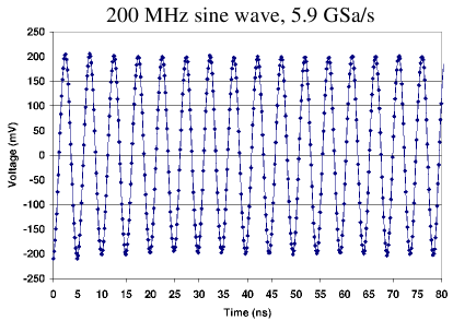
To illustrate how this performance corresponds into the ability to sample an RF sine wave, consider the uncalibrated waveform of Fig. 12. As the noise is small, deviations from a smooth curve give an indication of the level of calibration required in the following precision timing section.
4.4 Leakage current
Because leakage current is a concern for long storage times, and the array contains a large number of samples, which potentially take a long period to read out completely, this issue was studied extensively. A measurement of the leakage current for all 64k sampling capacitors was performed. This measurement was done by terminating the BLAB1 analog input and reading out each cell repeatedly, without a write update, for 20 seconds. A summary histogram of the leakage current determined for all storage cells from a fit to each leakage current slope is plotted in Fig. 13.
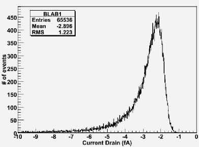
For reference, these values are in quite good agreement with leakage currents measured previously by our group for a similar TSMC CMOS process in different fabrication runs [13, 14]. If the effect of this leakage current is to be reduced to a level comparable with the noise, the following condition must be met:
| (5) |
where is the maximum storage to readout interval and is the pixel storage capacitance. Using a leakage current of = 25fA, which is conservatively larger than almost all storage cells, the maximum readout latency is thus
| (6) |
and is discussed in the readout speed subsection next. In general deep storage is needed for trigger latency buffering and a far smaller window of interest need only be read out.
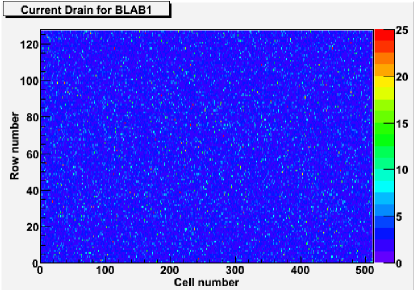
It had been posited that the more extreme leakage current values might correlate with the co-location of other logic or structures at the sampling array periphery. This conjecture is tested and rejected in Fig. 14, where the measured leakage current for each cell is plotted by array location. No obvious pattern is seen, and the values are consistent with being completely random.
4.5 Readout Speed
As mentioned earlier, there is flexibility in choice of the resolution versus speed trade-off. If determined to read out the entire array, the conversion cycle duration may be expressed as
| (7) |
where is the fixed latency (typically 50ns) associated with resetting the voltage ramp/changing addresses and is the interval required for the conversion to n-bits, given by the expression
| (8) |
for the 500MHz, dual-phase clock reference used in our measurements.
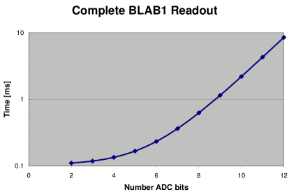
As mentioned previously, full chip readout is a rather extreme case. For a detector of the size of a typical high energy physics experiment, for “fast timing” signals, something like 100ns is the largest window required. Even for a multi-km scale radio neutrino detector, the aperture of interest would still only be in the s range, corresponding to less than 10% of the array, and for which the readout latency would be less than a millisecond. For a 100Hz radio trigger, or a 30kHz collision trigger, the deadtime is negligible for pipelined operation.
4.6 Power Dissipation
During sampling, the power dissipation can be as low as
| (9) |
where is the inverter transition charge and is 86ps at the nominal 5.8GSa/s sampling. During sampling all of the other biases may be disabled.
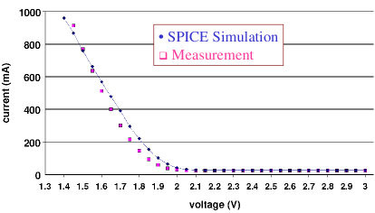
Quite unexpectedly, it was observed that lowering in the delay chain (running more slowly) dissipated more power, opposite of what the expression above would indicate. Below 2V, significantly more power was drawn. Returning to SPICE, it was found that indeed as the ROVDD is lowered, the leakage current of the inverters becomes important. In particular because of the decision to give each storage cell its own inverter pair. That multiplier proved to be a huge factor and precluded sustained low-speed sampling due to enormous power dissipation. Data and simulation agree qualitatively, though at large current draws it is likely the voltage drop in the finite resistance of the die power wiring becomes important (and ignored in simulation).
During readout, the current surges and the die subsequently heats substantially due to an oversight in the original design. While the comparator bias currents can be shut down during sampling, when conversion is required, they must all be operated. Again a large multiplier (64k comparators) applies, and even a A comparator bias leads to a 0.65A surge. This is addressed in future designs.
4.7 Concurrent Operation
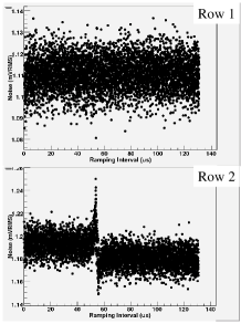
A key feature of the BLAB1 architecture is the ability to operate in a multi-hit buffer mode, to effectively reduce the deadtime to negligible levels. Concurrent readout while continuing to sample can have a deleterious impact on the quality of storage samples. Therefore we have performed a noise scan where the delay time of storage in Row 2 (adjacent row) is varied while Row 1 recording continues. The result appears in Fig. 17, where a small amount of cross-talk is observed right about the comparator transition time for Row 1. The effect is tiny (1 mV) and can be neglected.
As an example of the potential benefit, for a future 16 channel BLAB2 ASIC, where a 32ns window (320 samples at 10GSa/s) is recorded from each channel upon receipt of a Level 1 trigger, the net conversion time to 10 bits is roughly 160s if all these samples are read out. However, with an expected hit occupancy in the window for each ASIC (monitored by trigger out signal) of about 3.2%, the mean latency for readout is 5.12s. For a 30kHz maximum trigger rate, this is a 15.4% deadtime, though with large fluctuations. Having an 8 deep hold buffer for each channel (100ns wide), the probability of an overflow becomes a negligible .
5 Precision Timing Performance
Recent developments in high-density, high precision timing photodetectors are finding applications in Cherenkov detection techniques for particle identification, as well as medical imaging applications. To fully exploit the potential of these devices, robust performance, fine resolution timing and highly integrated readout electronics are needed. Over the decades a number of electronics techniques have been explored to maximize the timing performance of photodetector signals. These include Constant Fraction Discrimination, multi-level thresholding, charge integration for threshold timewalk correction, among a long list too extensive to adequately summarize here.
However, all of these techniques suffer from a number of practical limitations in actual application, which has served to degrade the realized performance. In the end, one simply cannot do better than having a high-fidelity “oscilloscope on a chip” for every sensor channel. Cost and data volume precluded this type of waveform recording until recent generations of SCA ASICs [5, 6, 7] demonstrated such techniques were practical, especially for large systems.
We present here some preliminary results of timing resolution tests with this BLAB1 ASIC. As these devices are distributed to interested users around the world, and more clever algorithms for improved timing performance are considered, further improvements on already promising results may be obtained.
5.1 Calibration
In order to address bin-by-bin timing width differences, a couple of different calibration techniques have been tried. The first utilizes a sine wave zero-crossing technique used for calibrating the LAB3 ASIC[5]. That technique works best when the frequency of the sine wave is such that the measured interval between zero crossings can be uniquely assigned to a limited number of bins between successive crossings.
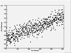
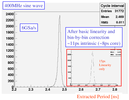
Due to intrinsic curvature limitations, this technique has an irreducible systematic error that is a function of sample rate. A more successful technique is to histogram the zero crossings of a sine wave and use the bin occupancy to derive the effective aperture width, the residual distribution is shown in Fig. 18. The most striking aspect of this distribution is the linear slope across the array. Applying only this linear slope correction leads to the 15ps RMS jitter in the determination of zero crossings for a subsequent sine wave data set, as seen in the inset distribution in Fig. 19. Applying a full bin-by-bin correction improves the distribution to 11ps RMS, with about an 8ps core.
5.2 Bench Test Signals
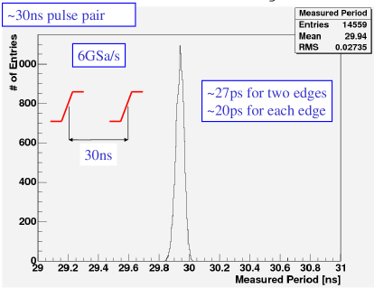
Timing performance was then evaluated using a pair of pulses separated by approximately 30ns. As seen in Fig. 20, over this longer timebase separation, a differential error of 27ps is obtained. The contribution of each edge then is then estimated as 27ps/, or 20ps per recorded edge.
For complex curvature along the leading edge of the signal, the timing resolution obtained is seen to be rather sensitive to the method choosen to characterize the signal “hit” time. Unless the photodetector signal is for a single p.e. quanta, the actual shape can be rather complex and dependent upon photon arrival statistics. Even in this simple case, noise and aperture systematics upon the leading edge can be important and can also be reduced by using multiple samples to fit to an analytic signal shape. In general, the estimate error can improve as something like 1/ for N samples along the leading edge. This is perhaps the most powerful aspect of having the full waveform samples to fit. Individual sampling errors can be averaged out. Examples are provided in the following subsection, where it is clear that at the sampling rates being studied, this waveform recording technique logs many samples on the leading edge, which can be used to improve the signal timing extraction.
5.3 PMT signal observation
A convenient feature of the BLAB1 ASIC is that a PMT output transmitted over a 50 coaxial cable can be directly connected to the BLAB1 input, as per the diagram of Fig. 1. Two example photodetector outputs, intended for fast-timing applications, are recorded in Fig. 21.
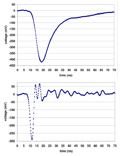
Both photodetectors specialize in fine time resolution and a direct comparison is informative. In the upper figure, the observed signal is an aggragate of a number of scintillation photons collected from a bar scintillator described in the next subsection. At bottom is the risetime of Micro-Channel Plate photodetector (MPC-PMT), intended for precise single photon detection. For future sub-10ps devices, the transit-time spread in the single p.e. amplification process may limit the ultimate resolution.
Finally affordable fast electronics may be able, on a channel-by-channel basis, to measure systematic variations and provide the requisite compensating corrections to achieve the penultimate resolution.
5.4 Belle TOF Counter
In order to evaluate the waveform sampler performance with a realistic set of pulses, we use cosmic muons incident on a spare TOF counter of the Belle detector [15]. The test set-up is illustrated in Fig. 22, and is located in the University of Hawaii Instrumentation Development Laboratory.
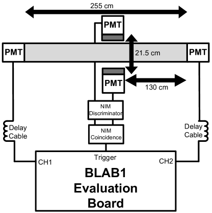
A sample of a few thousand cosmic ray muons were recorded using the test configuration shown in Fig. 22. PMT signals from both ends of the Bicron BC408 plastic scintillator bar are recorded. The bar is 4cm thick, 255cm long and viewed by Hamamatsu R6680 fine-mesh PMTs at each end. The Cherenkov trigger telescope counters consists of lucite slabs (approx. 5cm x 6cm x 3.5cm), also viewed by prototype R6680 fine-mesh PMTs. To estimate expected system performance, we recorded the trigger counters and extract an intrinsic error on determination of the trigger time by comparing the observed time difference in the two trigger counters. This jitter, as shown in Fig. 23, is quite large and should be improved in the future.
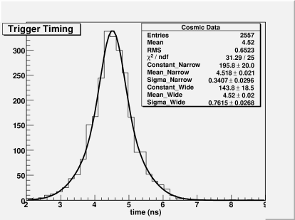
The contribution of the narrow gaussian can be subtracted in quadrature from the time difference observed at the ends of the Belle TOF counter, the distribution of which is shown in Fig. 24.
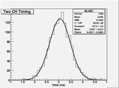
Doing this common mode subtraction leads to a resolution of about 190ps per PMT end. Comparing this observed signal resolution with a detailed Monte Carlo study [16], we can see that these values are comparable to the 150ps (170ps) or so for single end times from MC (data).
6 Future Directions
While the analog bandwidth of the BLAB1 is adequate for many RF recording applications, a higher bandwidth device will be explored, based upon the lessons learned from this first device. In particular, the tree structure and design of the analog amplifier tree is being scrutinized and improved in simulation. It is hoped that an almost arbitrarily large storage depth can be accommodated up to 1GHz of analog bandwidth through a careful layout of the buffer amplifier cascade array. In future devices, it is possible to significantly improve the number of storage cells. A specific example of the Particle Identification (PID) readout ASIC for the Belle upgrade is shown in Fig. 25.
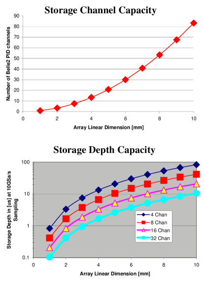
In the upper plot a s storage depth is assumed, or 40,000 storage cells at 10GSa/s. In the lower plot, four separate curves indicate the number of input channels and their subsequent depth versus array linear distance (assumed to be square). A die larger than 1cm per side was not considered for yield reasons. Also, pin constraints, particularly on making the output parallel to reduce readout latency, probably limit the practical number of input channels to 16. It is noted that many photodetectors operate at gains requiring additional amplification in order to provide a signal with sufficient amplitude for either triggering or recording. Integration of transimpedance and other input amplifier topologies are being studied and results from future devices that use such on-chip, high analog bandwidth elements will be reported later.
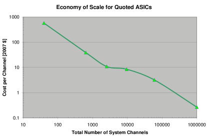
There is a misconception that waveform sampling is significantly more expensive than traditional discriminator + TDC methods. Certainly when packaged as a full oscilloscope and sold as a commercial unit, with large buffer depth, this can be true. In Fig. 26 is listed the fabricated and quoted prices during the 2007 fiscal year in the same TSMC 0.25m process. It is interesting to note that the slope of the first 3 devices correspond to Multi-Project Wafer runs, and the latter 3 are dedicated wafer runs. Packaging is not included and is a minimum of about $1/die in high volume.
A summary of active ASIC designs inspired by the performance of the BLAB1 ASIC may be found in Table 2.
| ASIC | # | Samples | Rate | BW | power |
| Acronym | Chan | per Chan | [GSa/s] | [GHz] | mW/chan |
| BLAB2 | 16 | 2k | 2-10 | 1 | |
| TARGET | 16 | 4k | 0.5-1 | 0.5 | |
| RAL64 | 64 | 512 | DC - 5 | 0.3 | |
| APTD | 4 | 8k | DC - 0.5 | 0.2 | |
| BIRD | 1 | 256k | 1 | 0.5 |
These devices find application niches for the following reasons:
-
•
Timing Performance BLAB2 is intended for sub-10ps photodetector pulse time recording
-
•
Low Cost TARGET is intended for the low-cost instrumentation of 1M photodetector channels of a future TeV telescope
-
•
High Density RAL64 is a dense array readout device, where 128 channels or more could be considered in the future
-
•
Low Power APTD is a demonstrator low-power ADC device for a proposed Advanced Pair Telescope satellite
-
•
Extended Depth BIRD is a very deep storage ASIC for the future IceRay extended radio neutrino detector at the South Pole
A number of these designs are reaching maturity and two have already been submitted for fabrication. Details of the designs and results from operation of these devices will be reported in the future.
7 Summary
A first generation of deep-storage Switched Capacitor Array (SCA) CMOS device has been studied in a 0.25m process. This architecture is optimized for concurrent acquisition and readout, permitting deadtimeless operation. Demonstrated low-power, high-resolution and exquisite timing performance make this device and subsequent variants attractive for readout of a broad range of particle and astroparticle detectors.
8 Acknowledgements
The authors gratefully acknowledge the generous support of the MOSIS Educational Program, which provided the fabrication of the BLAB1 ASIC prototype through their University Research Program. Testing was supported in part by Department of Energy Advanced Detector Research Award # DE-FG02-06ER41424.
References
- [1] P.W. Gorham et al., Phys. Rev. D 72, 023002 (2005).
- [2] D.Seckel and T. Stanev, Phys. Rev. Lett. 95, 141101 (2005).
- [3] S. Hashimoto (ed.) et al., KEK-Report-2004-4 (2004).
- [4] T. Tsuboyama et al., Nucl. Inst. Meth. A 541 421 (2005).
- [5] G.S. Varner, L.L. Ruckman, J.W. Nam, R.J. Nichol, J. Cao, P.W. Gorham, M. Wilcox, ”The large analog bandwidth recorder and digitizer with ordered readout (LABRADOR) ASIC,” Nucl. Inst. Meth. A 583 447 (2007).
- [6] S. Kleinfelder, IEEE Trans. Nucl. Sci. 50 (2003) 955.
- [7] C. Brönnimann, R. Horisberger and R. Schnyder, Nucl. Instr. Meth. A420 (1999) 264.
- [8] S. Ritt, Nucl. Instr. Meth. A518 (2004) 470.
- [9] G. Varner, Journal Instr. 1 (2006) P07001.
- [10] G. Varner, L. Ruckman, J. Schwiening and J. Va’vra, “Compact, Low-power and Precision Timing Photodetector Readout,” PoS (PD07) 026.
- [11] wxWidgets is a cross-platform GUI and tools library for GTK, Linux, MS Windows, and MacOS. www.wxwidgets.org
- [12] For example the ADC08D1500 from National Semiconductor, which digitizes two channels at 1.5GSa/s to 7.2 effective bits of resolution while consuming 1.9Watts.
- [13] G. Varner et al., Nucl. Inst. Meth. A 541 166 (2005); Int. J. Mod. Phys. A20:3808-3810, 2005.
- [14] M. Barbero, G. Varner et al., IEEE Trans. Nucl. Sci. 52 1187 (2005).
- [15] H. Kichimi et al., Nucl. Instr. Meth. A 453 315-320 (2000).
- [16] J.W. Nam et al., Nucl. Instr. Meth. A 491 54-68 (2002).