Enhanced annealing, high Curie temperature and low-voltage gating in (Ga,Mn)As: A surface oxide control study
pacs:
75.50.Pp, 81.05.Ea, 85.75.Hh(Ga,Mn)As and related diluted magnetic semiconductorsMatsukura et al. (2002); Jungwirth et al. (2006) play a major role in spintronics research because of their potential to combine ferromagnetism and semiconducting properties in one physical system. Ferromagnetism requires % of substitutional MnGa. Unintentional defects formed during growth at these high dopings significantly suppress the Curie temperature. We present experiments in which by etching the (Ga,Mn)As surface oxide we achieve a dramatic reduction of annealing times necessary to optimize the ferromagnetic film after growth, and report Curie temperature of 180 K at approximately 8% of MnGa. Our study elucidates the mechanism controlling the removal of the most detrimental, interstitial Mn defect. The limits and utility of electrical gating of the highly-doped (Ga,Mn)As semiconductor are not yet established; so far electric-field effects have been demonstrated on magnetization with tens of Volts applied on a top-gate, field effect transistor structure.Chiba et al. (2006) In the second part of the paper we present a back-gate, n-GaAs/AlAs/GaMnAs transistor operating at a few Volts. Inspired by the etching study of (Ga,Mn)As films we apply the oxide-etching/re-oxidation procedure to reduce the thickness (arial density of carriers) of the (Ga,Mn)As and observe a large enhancement of the gating efficiency. We report gatable spintronic characteristics on a series of anisotropic magnetoresistance measurements.
(Ga,Mn)As samples employed in our study were grown by low-temperature (C) molecular beam epitaxy. While the non-equilibrium growth is necessary for avoiding Mn precipitation at concentrations well above the solubility limit, it inevitably leads to the formation of a large number of metastable defects.Matsukura et al. (2002); Jungwirth et al. (2006) It is now firmly established that the most important unintentional impurities are interstitial Mn atomsMáca and Mašek (2002); Yu et al. (2002) which act as compensating donors and reduce the magnetic moment by forming antiferromagnetically coupled pairs with substitutional MnGa acceptors. In highly doped (Ga,Mn)As the fraction of interstitial Mn becomes significantJungwirth et al. (2005) with a largely detrimental effect on ferromagnetism and electrical conduction.
Interstitial Mn impurities can be removed by post-growth annealing at temperatures close to the growth temperature, while keeping the substitutional MnGa ions in place.Yu et al. (2002); Edmonds et al. (2002); Chiba et al. (2003); Ku et al. (2003); Stone et al. (2003) A number of complementary experiments have concluded that interstitial Mn ions out-diffuse during annealing towards the (Ga,Mn)As surface. Nevertheless, whether the mechanism limiting the diffusion has its origin in the (Ga,Mn)As bulk or in the surface oxide has remained a controversial open problem.Stone et al. (2003); Chiba et al. (2003); Kirby et al. (2005); Malfait et al. (2005); Edmonds et al. (2004); Adell et al. (2005); Sadowski et al. (2006); Kirby et al. (2006); Holý et al. (2006) Figures 1 and 2 provide a resolution to this question and show that it has important consequences for the efficiency of the post-growth optimization of magnetic properties of the material.
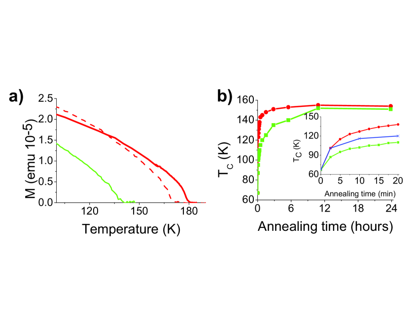
Figure 1(a) shows SQUID magnetization measurements on a 35 nm (Ga,Mn)As film with 11% nominal Mn-doping. The annealing was performed in air by placing the sample on a hot plate with temperature 200∘C. Two different annealing procedures are compared for samples cleaved from the same wafer which was rotated during growth to ensure homogeneity across the epilayer. Beside the standard continuous annealing, a sequence of discrete etch-anneal steps has been applied, each consisting of 30 s etching in 30% HCl, rinsing in water, and subsequent annealing at 200∘C for 5 min. With continuous annealing, the as-grown Curie temperature 85 K is increased to 137 K after 15 min of annealing and a maximum K is reached in 100 min. By employing the etch-anneal technique, is reached in 15 min, and a saturated value of K is obtained in 40 min. We see a large reduction of the annealing time due to surface-oxide etching. The procedure also yields a sizable increase of the maximum attainable Curie temperature in the material. Our K represents an increase of the record Curie temperature achieved in (Ga,Mn)As to dateJungwirth et al. (2005) by 7 K and is the highest reported for uniform, carrier-mediated (III,Mn)V ferromagnet. The MnGa density for the sample is estimated to 8% and the value, when compared with a series of our other as-grown and annealed materials of a wide range of Mn dopings, shows no indication of reaching a Curie temperature limit in (Ga,Mn)As.
In Figure 1(b) we present a detailed investigation of the etch-anneal process. To demonstrate that our findings are generic we show results for a standard, 7% Mn-doped 50 nm thick (Ga,Mn)As epilayer. In the main panel of Figure 1(b) we compare two sets of SQUID Curie temperature measurements as a function of annealing time, one for continuous annealing and the other for the etch-anneal procedure. In the inset, we compare these two measurements with annealing of the sample exposed to a single etching before the first annealing step. The presence of the surface oxide layer clearly plays the crucial limiting role in the (Ga,Mn)As annealing process. By repeating several etch-anneal steps instead of annealing continuously, the post-growth treatment time for reaching maximum , around 150 K in this particular wafer, is slashed by a factor of 10. Furthermore, the inset indicates that the oxide layer formed after growth, which very rich in Mn as discussed below, and the oxide layer regrown on a clean (Ga,Mn)As surface during annealing are comparably efficient in blocking the interstitial Mn removal.
Without passivation of out-diffused Mn-ions by oxidation (or nitridation, etc.), the diffusion of the interstitial Mn towards the (Ga,Mn)As free surface is inhibited by the formation of an electrostatic barrier.Stone et al. (2003); Chiba et al. (2003); Kirby et al. (2005); Malfait et al. (2005); Adell et al. (2005); Sadowski et al. (2006) From this perspective the key role of the surface oxide in the annealing process is plausible as it might prevent the Mn-ions and free oxygen from interacting with each other. It is a generic feature, related to the shorter (by 20%) metal-oxygen bond length compared to GaAs, less interstitial space, and amorphous structure, that the impurity diffusion channels through the oxide are effectively blocked.Åhman et al. (1996) To investigate the structure of the oxide layer and the Mn-ion passivation process in more detail we performed a series of complementary x-ray photoemission spectroscopy (XPS), magnetization, and transport measurements.
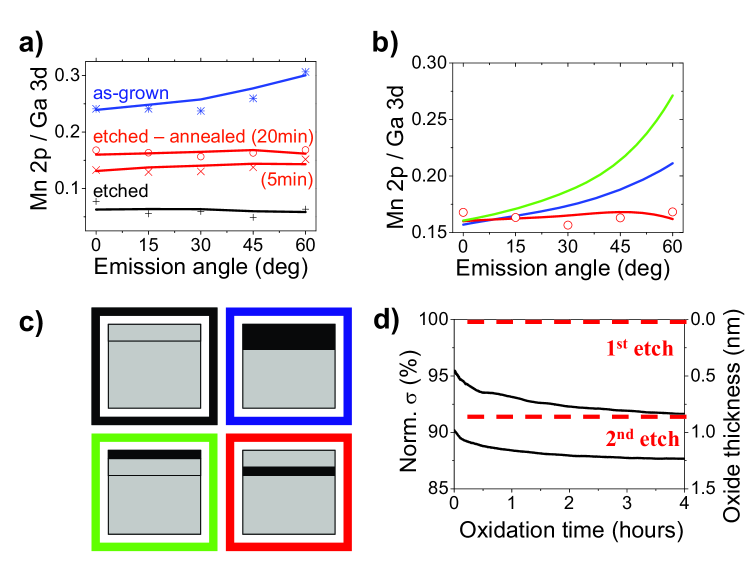
The angular dependent XPS study was done on a 50 nm (Ga,Mn)As epilayer with 8% Mn-doping from which we prepared four different samples: a piece of an as-grown material, a sample once etched after growth and unannealed, a piece etched and annealed for 5 min, and another sample etched and annealed for 20 min. Ga-, Mn-, and O- photoelectron line intensities were recorded with the angle-dependent probing depth upto 3 nm, and we used SESSA software package to simulate the XPS data. The fit of the measured O-/Ga- ratios yields 9 Å thickness of the oxidized (Ga,Mn)As layer in the as-grown material; in the etched unannealed sample, measured 30 min after etching, the fitted oxidized layer thickness is 5.3 Å(comparable to results of XPS measurements in pure GaAs.Storm et al. (1994)). The angular dependencies of the Mn-/Ga- ratio for the four studied samples are plotted in Figure 2(a). The best fit for the as-grown material is obtained assuming 8.8% Mn concentration in the unoxidized (Ga,Mn)As, which is consistent with the nominal Mn-doping, and a 44% Mn concentration in the 9 Å surface oxide. In the etched unannealed samples the same fitted values of 8.8% Mn are found in the 5.3 Å oxidized layer and in the (Ga,Mn)As film underneath. This indicates that after etching off the Mn-rich surface layer formed during growth, a thinner layer of (Ga,Mn)As is oxidized without any marked redistribution of Mn throughout the (Ga,Mn)As epilayer.
The analysis of the etched and 20 min annealed sample, which shows a sizable reemergence of Mn at the surface due to annealing, is detailed in Figure 2(b). To fit the corresponding XPS data we considered a Mn rich layer on top of the oxide, a uniform distribution of Mn in the Mn-rich oxide, and a Mn-rich layer at the interface of the oxide and unoxidized (Ga,Mn)As (see Figure 2(c)). Clearly the last model provides the best fit to the measured data with an average thickness of the Mn-rich interfacial layer of 2 Å. We conclude that the Mn passivation takes place at the bottom of the oxide layer by oxygen which has diffused through the oxide and reached the interface with (Ga,Mn)As. Note that the picture is consistent with previous studies of GaAs oxidation which found a substantially smaller diffusivity through the oxide film of metal atoms as compared to oxygen.Wolan et al. (1998)
Complementary estimates of the oxide thickness based on measured reduction of the magnetic moment and sheet conductance, which can be readily performed in highly-doped thin (Ga,Mn)As films, are consistent with the XPS analysis. In Figure 2(d) we show two subsequent measurements of the time-dependent room-temperature resistance of a nominally 10 nm, 8% Mn-doped (Ga,Mn)As wafer. Each experiment started with etching the surface oxide and then, after two minutes, we began monitoring for several hours the time evolution of the resistance due to re-oxidation of the (Ga,Mn)As surface. Oxide layer thicknesses were obtained by assuming ohmic conduction in the unoxidized (Ga,Mn)As. In a few minutes after etching, a several Angstrom thick oxide layer quickly forms at the surface, followed by a significantly lower-rate oxidation process in which the thickness of the oxide reaches 1 nm in several hours. Oxide etching and subsequent re-oxidation can therefore be used for a controllable thinning of (Ga,Mn)As films in sub-nm steps when studying numerous scaling characteristics of ferromagnetic semiconductors with the film thickness and arial density of carriers. Gating of ultrathin (Ga,Mn)As epilayers, discussed in the remaining paragraphs, is one example where this simple table-top technique can be utilized.
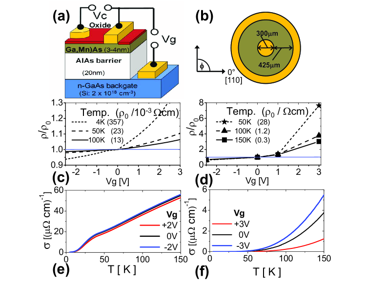
In Figures 3(a) and (b) we show schematics of our (Ga,Mn)As field effect transistor (FET) heterostructure together with the top-view of the Corbino geometry of the source and drain electrodes used for transport measurements. A heavily doped epitaxial n-GaAs buffer layer grown on an n-type substrate forms the gate electrode which is separated from the (Ga,Mn)As film by a 20 nm thick AlAs barrier. An appreciable gate action is expected for hole depletion/accummulation of cm-3 which in our geometry is achieved at gate voltages of a few Volts for (Ga,Mn)As thicknesses of 5 nm and lower. This is about an order of magnitude smaller voltage as compared to previous experiments in top-gate (Ga,Mn)As/Al2O3/metal FETs.Chiba et al. (2006) Furthermore, because of the free (Ga,Mn)As surface in our back-gate FET, the structure is directly compatible with the oxide-etching technique.
Figures 3(b) and (c) show two gating characteristics of the resistance of one physical device in which the Corbino contacts were first patterned by optical lithography on a 4 nm thick (plus a 1 nm oxidized surface layer), 8% Mn-doped (Ga,Mn)As. After measuring this device, the (Ga,Mn)As layer was further etched to approximately 3 nm without removing the contacts, and again measured. In both cases we find a decrease/increase of the (Ga,Mn)As channel conductance upon depletion/accummulation induced by gating. (Note that the asymmetry between positive and negative gate voltage characteristics reflects the p-n junction nature of our FET.) The gating efficiency is enhanced in the thinned sample, consistent with the reduced arial density of carriers. We attribute the large amplification of this effect with decreasing temperature to the vicinity of the metal-insulator transition in the studied (Ga,Mn)As film.
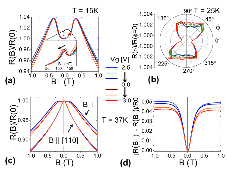
Detailed measurements of gate-dependent magnetoresistance (MR) characteristics were performed in the 4 nm (Ga,Mn)As transistor to investigate its utility as a three-terminal spintronic device and as a new tool for exploring the dependence of magnetotransport in a ferromagnet on carrier concentration. The source-gate leakage current in the device is negligible compared to the source-drain current for gate voltages in the range from -2.5 to +3 V at temperatures larger than 4 K. Examples of the rich MR phenomenology we observe are shown in Figure 4. In panel (a) we plot MR curves for magnetic fields oriented nearly perpendicular to the (Ga,Mn)As plane. The high-field gate dependent MRs are discussed below. In this plot we highlight (see the inset) the low-field switching event in the in-plane magnetization component, reflected as a peak on the MR traces at about 120 mT whose position moves by 10’s of mT between depletion and accumulation. In-plane magnetization rotation experiments shown in Figure 4(b) illustrate that besides the magnetic anisotropies also the in-plane anisotropic magnetoresistance (AMR) is modified by the gate. In the Corbino geometry with in-plane field the non-crystalline AMR component given by the relative angle between current and magnetization is expected to average to zero so the measured signal corresponds to the typically more subtle crystalline AMR terms.Rushforth et al. (2007) We find that even these terms are sensitive to depletion or accumulation of holes achieved in our (Ga,Mn)As FET structure. Larger crystalline AMR we observe for depletion is qualitatively consistent with theoretically expected trends for magnetocrystalline anisotropy coefficients in (Ga,Mn)As.Rushforth et al. (2007)
Stronger gate-dependence of MR signals is observed when magnetization is rotated from the in-plane, magnetic easy direction towards the out-of-plane hard axis. In Figure 4(c) we compare field-sweep measurements for in-plane magnetic fields and for the perpendicular-to-plane fields. Since magnetization is expected to remain parallel with the field in the former experiment, the trace is interpreted as the isotropic negative MR for which we find only a very week dependence on the gate voltage. By subtracting the isotropic MR part from the curves measured in the perpendicular-to-plane magnetic field sweeps we obtain the out-of-plane AMRs (see Figure 4(d)), i.e., the difference between resistances for the in-plane magnetization orientation at low fields and for the out-of-plane orientation at high saturating fields. Unlike the in-plane AMR, here the non-crystalline AMR component is present even in the Corbino geometry and we see that the AMR decreases from 5% at -2.5 V (accumulation) to 4% at 3 V (depletion), again qualitatively consistent with theoretically expected trends for the non-crystalline AMR.Rushforth et al. (2007) Note that part of the out-of-plane MR may be due to the anomalous Hall effect whose contribution cannot be directly separated from the AMR in the Corbino device. Nevertheless, since the anomalous Hall (and normal Hall at 1 T) resistance is typically much smaller than the sheet resistance in (Ga,Mn)As, the AMR is likely the dominant contribution to MR traces in Figure 4(d).
To summarize we have presented several advancements towards functional (Ga,Mn)As ferromagnetic semiconductors for spintronics. By introducing the etch-anneal post-growth treatment we have significantly enhanced the out-diffusion of compensating interstitial Mn defects and elucidated the basic mechanism controlling their passivation at the surface. The technique helped us to prepare (Ga,Mn)As material with the highest Curie temperature reported to date within the family of bulk (III,Mn)V carrier-mediated ferromagnets. Electrical gating of ultra-thin (Ga,Mn)As films was explored on a back-gate, all-semiconductor (Ga,Mn)As FET. The device operates at gate voltages of a few Volts. Its free (Ga,Mn)As surface geometry allows for a controllable thinning of the (Ga,Mn)As layer in sub-nanometer steps by etching and re-oxidation, resulting in a significant enhancement of the gating efficiency. Our observations of gate-dependent crystalline and non-crystalline AMR responses open new ways for exploring MR effects in ferromagnets and prototype realizations of three-terminal spintronic devices.
We acknowledge fruitful collaborations with R. P. Campion, M. Cukr, B. L. Gallagher, M. Maryško, and J. Zemek, and support from EU Grant IST-015728, from Grant Agency and Academy of Sciences and Ministry of Education of the Czech Republic Grants FON/06/E001, FON/06/E002, AV0Z1010052, KAN400100652, and LC510.
References
- Matsukura et al. (2002) F. Matsukura, H. Ohno, and T. Dietl, in Handbook of Magnetic Materials, edited by K. H. J. Buschow (Elsevier, Amsterdam, 2002), vol. 14, p. 1.
- Jungwirth et al. (2006) T. Jungwirth, J. Sinova, J. Mašek, J. Kučera, and A. H. MacDonald, Rev. Mod. Phys. 78, 809 (2006).
- Chiba et al. (2006) D. Chiba, F. Matsukura, and H. Ohno, Appl. Phys. Lett. 89, 162505 (2006).
- Máca and Mašek (2002) F. Máca and J. Mašek, Phys. Rev. B 65, 235209 (2002).
- Yu et al. (2002) K. M. Yu, W. Walukiewicz, T. Wojtowicz, I. Kuryliszyn, X. Liu, Y. Sasaki, and J. K. Furdyna, Phys. Rev. B 65, 201303 (2002).
- Jungwirth et al. (2005) T. Jungwirth, K. Y. Wang, J. Mašek, K. W. Edmonds, J. König, J. Sinova, M. Polini, N. A. Goncharuk, A. H. MacDonald, M. Sawicki, et al., Phys. Rev. B 72, 165204 (2005).
- Edmonds et al. (2002) K. W. Edmonds, K. Y. Wang, R. P. Campion, A. C. Neumann, N. R. S. Farley, B. L. Gallagher, and C. T. Foxon, Appl. Phys. Lett. 81, 4991 (2002).
- Chiba et al. (2003) D. Chiba, K. Takamura, F. Matsukura, and H. Ohno, Appl. Phys. Lett. 82, 3020 (2003).
- Ku et al. (2003) K. C. Ku, S. J. Potashnik, R. F. Wang, M. J. Seong, E. Johnston-Halperin, R. C. Meyers, S. H. Chun, A. Mascarenhas, A. C. Gossard, D. D. Awschalom, et al., Appl. Phys. Lett. 82, 2302 (2003).
- Stone et al. (2003) M. B. Stone, K. C. Ku, S. J. Potashnik, B. L. Sheu, N. Samarth, and P. Schiffer, Appl. Phys. Lett. 83, 4568 (2003).
- Kirby et al. (2005) B. J. Kirby, J. A. Borchers, J. J. Rhyne, K. V. O’Donovan, T. Wojtowicz, X. Liu, Z. Ge, S. Shen, and J. K. Furdyna, Appl. Phys. Lett. 86, 072506 (2005).
- Malfait et al. (2005) M. Malfait, J. Vanacken, W. Van Roy, G. Borghs, and V. V. Moshchalkov, Appl. Phys. Lett. 86, 132501 (2005).
- Edmonds et al. (2004) K. W. Edmonds, P. Boguslawski, K. Y. Wang, R. P. Campion, N. R. S. Farley, B. L. Gallagher, C. T. Foxon, M. Sawicki, T. Dietl, M. B. Nardelli, et al., Phys. Rev. Lett. 92, 037201 (2004).
- Adell et al. (2005) M. Adell, J. Kanski, L. Ilver, V. Stanciu, and P. Svedlindh, Phys. Rev. Lett. 94, 139701 (2005).
- Sadowski et al. (2006) J. Sadowski, J. Z. Domagala, V. Osinniy, J. Kanski, M. Adell, L. Ilver, C. Hernandez, F. Terki, S. Charar, and D. Maude (2006), eprint arXiv:cond-mat/0601623.
- Kirby et al. (2006) B. J. Kirby, J. A. Borchers, J. J. Rhyne, K. V. O’Donovan, S. G. E. te Velthuis, S. Roy, C. Sanchez-Hanke, T. Wojtowicz, X. Liu, W. L. Lim, et al., Phys. Rev. B 74, 245304 (2006).
- Holý et al. (2006) V. Holý, Z. Matěj, O. Pacherová, V. Novák, M. Cukr, K. Olejník, and T. Jungwirth, Phys. Rev. B 74, 245205 (2006).
- Åhman et al. (1996) J. Åhman, G. Svensson, and J. Albertsson, Acta Cryst. C52, 1336 (1996).
- Storm et al. (1994) W. Storm, D. Wolany, F. Schröder, G. Becker, B. Burkhardt, L. Wiedmann, and A. Benninghoven, J. Vac. Sci. Technol. B 12, 147 (1994).
- Wolan et al. (1998) J. T. Wolan, C. K. Mount, and G. B. Hoflund, Appl. Phys. Lett. 72, 1469 (1998).
- Rushforth et al. (2007) A. W. Rushforth, K. Výborný, C. S. King, K. W. Edmonds, R. P. Campion, C. T. Foxon, J. Wunderlich, A. C. Irvine, P. Vašek, V. Novák, et al., Phys. Rev. Lett. 99, 147207 (2007).