Influence of Functional Groups on Charge Transport in Molecular Junctions
Abstract
Using density functional theory (DFT), we analyze the influence of five classes of functional groups, as exemplified by NO, OCH, CH, CCl, and I, on the transport properties of a 1,4-benzenedithiolate (BDT) and 1,4-benzenediamine (BDA) molecular junction with gold electrodes. Our analysis demonstrates how ideas from functional group chemistry may be used to engineer a molecule’s transport properties, as was shown experimentally and using a semiempirical model for BDA [Nano Lett. 7, 502 (2007)]. In particular, we show that the qualitative change in conductance due to a given functional group can be predicted from its known electronic effect (whether it is / donating/withdrawing). However, the influence of functional groups on a molecule’s conductance is very weak, as was also found in the BDA experiments. The calculated DFT conductances for the BDA species are five times larger than the experimental values, but good agreement is obtained after correcting for self-interaction and image charge effects.
| Functional | Structure | Electronic | Other | |
|---|---|---|---|---|
| Group | Effect | Examples | ||
| NO | nitro | withdrawal | CN, COR, | |
| SOR | ||||
| OCH | methoxy | donation | NR, OR | |
| CH | methyl | donation | CH5, CH7 | |
| alkyls | ||||
| CCl | trichloromethyl | withdrawal | CF, NR | |
| I | iodo | withdrawal & | F, Cl, Br | |
| donation | halogens | |||
One of the main advantages of molecular based electronics over present day semiconductor technology is the vast flexibility in design and functionality offered by the myriad of available molecules Joachim et al. (2000). In order to fully exploit this flexibility for the synthesis of molecular devices, it is vital to establish simple guiding rules to estimate the effect that a given change in the molecule’s composition or conformation has on its electrical properties.
So far, most experimental and theoretical work on single-molecule conduction has focused on understanding the basic properties of individual junctions Reed et al. (1997); Stokbro et al. (2003); Xu and Tao (2003); Stadler et al. (2005). On the other hand, few studies have aimed at describing general trends across molecular species Venkataraman et al. (2006); Chen et al. (2006); Reichert et al. (2002).
It is well known that the chemistry of a functional parent or parent molecule may be altered in a consistent manner by the attachment of functional groups Clayden et al. (2001). Further, the influence of a particular functional group on a parent molecule’s chemistry may be predicted qualitatively by considering the electronic effect of the functional group.
We will demonstrate how such ideas may also be applied to describe the influence of a functional group on a parent molecule’s transport properties. This was recently shown experimentally for BDA, and the results were explained by scaling the molecule’s empirical conductance value by the calculated ionization potentials in the gas phase for the BDA species with two bonded Au atoms Venkataraman et al. (2007). By employing these concepts from functional group chemistry, we may engineer the electronic transport properties of a known functional parent. This may be done using a functional group whose frontier orbitals have the same symmetry as the conducting orbital of the parent molecule ( or ). Groups with donating/withdrawing electronic effects may then be used to raise/lower the eigenenergy of the conducting orbital.
In this paper, we analyze the influence of functional groups on the conductance of both a 1,4-benzenedithiolate (C6H4S or BDT) and a 1,4-benzenediamine (C6H4(NH) or BDA) molecular junction between gold contacts. We consider these molecules because BDT is perhaps the best studied molecule for charge transport Reed et al. (1997); Stokbro et al. (2003); Xiao et al. (2004), while the influence of functional groups on the BDA molecule has been recently studied experimentally Venkataraman et al. (2007). In particular, we shall consider prototypical functional groups from each of the five electronic categories, as shown in Table 1. These categories are: (1) withdrawal by conjugation through the network ( withdrawal), (2) donation by conjugation through the network ( donation), (3) donation by inductive effect through the network ( donation), (4) withdrawal by inductive effect through the network ( withdrawal), and (5) withdrawal by inductive effect through the network with donation by conjugation through the network ( withdrawal & donation) Clayden et al. (2001). For each electronic effect categorization we have selected as respective examples a nitro group (NO), a methoxy group (OCH), a methyl group (CH), a trichloromethyl group (CCl), and an iodo group (I). Other examples of functional groups from each category are also provided in Table 1.
All calculations have been performed using the SIESTA density functional theory (DFT) code Soler et al. (2002) with the PBE exchange correlation (xc) functional Perdew et al. (1996), a double zeta polarized (DZP) basis set, and a mesh cutoff of 200 Ry. We first adsorbed the molecules on a five layer thick gold (111) slab and relaxed the molecule and the three outermost surface layers. The supercell contained 33 gold atoms in the surface plane, within which we used 22 -points. A pyramid of four gold atoms attached to the five layers of gold (111) was then introduced in the supercell to simulate the tip of a scanning tunneling microscope (STM). The pyramid was placed with its apex atom close to the unbound S/N atom of the molecule, and upon further relaxation the molecule bonds to the gold apex atom, as shown in Fig. 1.
In this way we model a low temperature conductance measurement for a low molecular coverage on a gold (111) surface using an STM tip F. Chen et al. (2007). Such a configuration may not accurately describe the results of break-junction experiments, especially for the weakly bound BDA species Quek et al. (2007). However, as shown in Ref. Quek et al., 2007, such a binding site yields a similar transmission function to more energetically favorable geometries. Thus, our chosen geometry should allow us to discern more broadly applicable trends in the electronic effects of the functional groups, which are our primary interest.
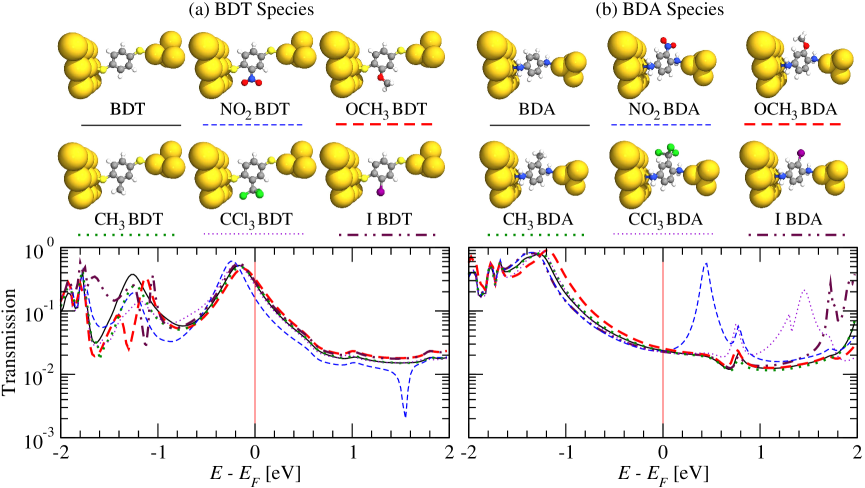
We find that the BDT species (BDT, NOBDT, OCHBDT, CHBDT, and I BDT) prefer the bridge site of the (111) surface and are rotated by approximately 30∘ to the surface normal Bratkovsky and Komilovitch (2003), as shown in Fig. 1(a). On the other hand, we find that the BDA species (BDA, NOBDA, OCHBDA, CHBDA, and I BDA) prefer the atop site and lie down at an angle of approximately 50∘ to the surface normal Quek et al. (2007), as shown in Fig. 1(b).
Having chosen the contact geometries, we calculated the elastic transmission functions using the non-equilibrium Green’s function (NEGF) formalism. The calculation procedure is equivalent to the one described in Ref. Thygesen and Jacobsen, 2005, except that the Hamiltonian was represented in the SIESTA atomic orbital basis instead of Wannier functions. We note here that the DZP SIESTA basis set has recently been shown to yield transmission functions in quantitative agreement with plane wave codes and maximally localized Wannier functions Strange et al. (2008). The transmission function was averaged over four -points in the surface plane, and three gold (111) layers were added on both sides of the molecule before the system was coupled to the bulk leads to ensure a smooth matching of the effective DFT potential.
The calculated transmission functions are shown in Fig. 1. For both BDT and BDA the change in the transmission function, , near the Fermi level when the functional groups are attached, is strikingly small.
| BDT Species | [] | BDA Species | [] |
|---|---|---|---|
| BDT | 0.28 | BDA | 0.024 |
| NOBDT | 0.16 | NOBDA | 0.024 |
| OCHBDT | 0.32 | OCHBDA | 0.026 |
| CHBDT | 0.29 | CHBDA | 0.024 |
| CClBDT | 0.25 | CClBDA | 0.022 |
| IBDT | 0.29 | IBDA | 0.023 |
The calculated conductances, , where , for the BDT and BDA species are shown in Table 2. As is often the case for DFT transport calculations on molecular contacts, our results differ substantially from the experimental values of 0.011 obtained for BDT Xiao et al. (2004), and 0.0064 for BDA Quek et al. (2007). We will address this issue in the last part of the paper. At this point, we observe that functional groups whose valence orbitals are of symmetry seem to have the most influence on the molecule’s conductance, with the withdrawing group lowering the conductance, and the donating group raising the conductance.

For both BDT and BDA species, we found that transport primarily occurs through the HOMO, which in both cases is a bonding molecular orbitals, as shown in Fig. 2. In principle, the concept of molecular orbitals is somewhat artificial for a chemisorbed molecule, as hybridization effects will broaden the levels into resonances. One way of generalizing the concept is to consider , the projection of the Hamiltonian of the contacted system onto the subspace spanned by the basis functions of the molecule. The eigenvectors of can be regarded as molecular orbitals renormalized by the electrodes Thygesen and Jacobsen (2005). For molecules which are not too strongly coupled to the electrodes, these renormalized molecular levels are easily identified with the levels of the free molecule.
In Fig. 2 we compare the position of the HOMO level (relative to ) of the contacted molecules with the HOMO level (relative to vacuum) of the free gas phase molecules. The variation in the HOMO position with the functional group correlates directly with the variation in the conductance (see Table 2) which shows that the current is indeed carried by the HOMO. One exception from this trend is NOBDA for which the conductance is not lowered even though the HOMO is significantly down shifted. This is because the LUMO of NOBDA lies so low that it also contributes to the charge transport. From Fig. 2 we can also see that each functional group produces a remarkably consistent shift of the conducting orbital for BDA and BDT. This agrees with the basic premise of functional group chemistry, that a given functional group will alter different parent molecules in a consistent way. We also notice that the two groups (NO and OCH) give the largest shifts of the eigenenergies, while the functional groups with symmetry have little influence. Moreover, the withdrawing functional group () delocalizes the HOMO and thereby lowers the eigenenergy, while the donating functional group () confines the HOMO and thereby increases the eigenenergy. Thus the main ideas of functional group chemistry may be employed to qualitatively predict a functional group’s influence on a given functional parent’s conducting orbital(s).
We stress that the qualitative effect of the functional groups on the HOMO of the contacted molecule, and thus its conductance, roughly follows from the effect of the functional groups on the free molecule’s HOMO, as was found experimentally for BDA Venkataraman et al. (2007). This is significant, as it suggests that the latter could be used as a simple descriptor to estimate the impact of a given functional group on the conductance, thereby allowing for an efficient screening of large numbers of functional groups.
When we compare in Fig. 2 the magnitude of the shifts due to the functional groups for both BDT and BDA, we find significantly smaller effects for the contacted molecules than for the gas phase molecules. For example, the shift due to NO on BDT is approximately 0.4 eV in the gas phase, while it is less than 0.1 eV in the contact. This may be understood by recognizing that the gold contacts act as electron sources/sinks for the parent molecule, counteracting the functional group’s electronic influence. We thus believe that the weak influence of the functional groups on the conductance is a result of the self-consistent ‘pinning’ of the HOMO level which ensures the charge neutrality of the molecule. Such effects are indeed physical, but could be artificially enhanced by self-interaction errors in the PBE xc-functional: For partially occupied molecular orbitals, an incomplete cancellation of the Coulomb self interaction by the xc-functional will artificially raise (lower) the energy of that orbital when charge is added (removed) and this will enhance the ‘level pinning’.
Self interaction errors also contribute to the well-known underestimation of band gaps by DFT calculations Cai et al. (2002). Recently, an atomic self interaction correction (ASIC) scheme Filippetti and Spaldin (2003); Pemmaraju et al. (2007) has been proposed as a simple cure to this problem for molecular contacts. In general, however, image charges formed in the metallic electrodes when electrons are added to or removed from the molecule also renormalize the molecular levels Neaton et al. (2006), and this effect is not captured by the SIC.
| BDA Species | [] | [] | [] |
|---|---|---|---|
| BDA | 0.024 | 0.0035 | 0.0064111Ref. Venkataraman et al.,2007 |
| NOBDA | 0.024 | 0.0032 | — |
| OCHBDA | 0.026 | 0.0035 | 0.006911footnotemark: 1 |
| CHBDA | 0.024 | 0.0034 | 0.006411footnotemark: 1 |
| CClBDA | 0.022 | 0.0034 | — |
| ClBDA | 0.015 | 0.0025 | 0.006011footnotemark: 1 |
| IBDA | 0.023 | 0.0036 | — |
In Table 3 we compare our DFT calculated conductances for the BDA species with corresponding experimental values Venkataraman et al. (2007). The calculated numbers are roughly five times larger than the experimental ones due to the above mentioned deficiencies of the DFT approach. It is, however, interesting to notice that: (i) the weak effect of functional groups is found in both data sets (ii) the qualitative effect of the functional groups on the conductance (increase/decrease) is reproduced by calculations. In the second column of Table 3 we present the results of our conductance calculations after a ‘scissors operator’ (SO), which corrects for self-interaction errors and image charge effects, has been applied to the molecule’s spectrum.
To construct the SO we follow a recent work by Quek et al. who applied the scheme to a BDA-gold junction Quek et al. (2007). In this method, the underestimation of the DFT HOMO and LUMO are corrected by shifting the occupied/unoccupied orbitals of the contacted molecule by , where is the DFT HOMO level for the free molecule and the ionization potential LUM . We also calculate the later in DFT from , where is the total energy of the molecule with charge in the gas phase, while is the total energy in the gas phase of the neutral molecule. For BDA without functional groups we find 6.73 eV, which agrees quantitatively with the experimental value of 6.83 eV Quek et al. (2007). We found only small variations in for the different BDA species and have used -2.7 eV for all molecules, as indicated in Fig. 2.
To estimate the shift of the molecular levels by image charge effects, we first calculate the charge distribution after removing an electron from the free molecule. A Mulliken analysis is then used to approximate this continuous charge distribution by point charges located at the atoms of the molecule. We model the gold contacts as two perfectly conducting surfaces separated by 13.2 Å, which corresponds to the vacuum separation between the opposing gold (111) surfaces. We then obtain an image potential -0.9 eV for all of the BDA species considered sup . For the BDA molecular junctions, we thus shift all occupied/unoccupied orbitals (obtained by diagonalizing ) by 1.8 eV as indicated in Fig. 2. Calculating the conductance using the renormalized Hamiltonian yields the values shown in Table 3. We find that this ‘ad hoc’ correction produces results approximately half those obtained from break-junction experiments on the BDA species Venkataraman et al. (2007). This is most probably due to our choice of contact geometry, as our calculated conductance for BDA of 0.024 is about half the average DFT value calculated over 15 different break-junction contact geometries of 0.046 Quek et al. (2007). We stress, however, that the use of this SO can only be justified for weakly coupled molecules with HOMO/LUMO levels well separated from . In Fig. 2 we see this is the case for the BDA species, since the HOMOs are localized near the amine contact groups, providing a poor overlap with the gold contact orbitals. However, for the BDT species, whose HOMOs are rather diffuse around the sulfur atoms, there is a strong overlap with the gold contact orbitals, so that application of the SO is not justified.
In conclusion, we found that the ideas of functional group chemistry may be applied to qualitatively predict the influence of a functional group on the electronic structure of a parent molecule, as has been found for BDA both experimentally and using a semiempirical model Venkataraman et al. (2007). However, we also found that functional groups have a very weak influence on a molecule’s conductance in agreement with recent experiments Venkataraman et al. (2007). The reason for the weak influence is that charge neutrality pins the HOMO/LUMO molecular levels, making it difficult to shift them relative to . By applying multiple functional groups to the same parent molecule it may be possible to obtain a stronger influence, as was found for BDA Venkataraman et al. (2007). By employing a scissors operator correcting for self-interaction errors and image charge effects, we obtained qualitative agreement with experimental conductance values for the BDA species. Our results suggest that effective ‘switching’ of a molecule’s conductance may require a more direct change in the strength or geometry of the molecule’s contacts, to overcome the ‘level pinning’ of the metal.
We thank J. K. Nørskov, S. Dobrin, and M. Strange for useful discussions. The authors acknowledge support from the Danish Center for Scientific Computing through grant No. HDW-1103-06. The Center for Atomic-scale Materials Design (CAMD) is sponsored by the Lundbeck Foundation.
Appendix A Scissors Operator (SO)
The SO for a free molecule in the gas phase , is given by
| (1) |
where is the DFT HOMO level of the free molecule in the gas phase, and is its first ionization potential, which is defined as
| (2) |
Here is the total gas phase energy calculated for a molecule with charge , while is the total energy in the gas phase for the neutral molecule.
The occupied/unoccupied orbitals of the contacted molecule are shifted by the same amount for each orbital. This is reasonable for orbitals other than the HOMO and LUMO, since these orbitals are sufficiently far from the Fermi level to have little influence on the contacted molecule’s conductance.
However, this is not the case for the LUMO orbital, especially for NO2 BDA. In this case, a fully rigorous calculation would shift the DFT LUMO level by , where is the DFT LUMO level for the free molecule and the electron affinity. The later may be calculated similarly to the ionization potential in DFT from , where is the total energy of the molecule with charge in the gas phase. However, as discussed in Ref. Quek et al., 2007, when such a shift was calculated for the BDA LUMO, it was found to be approximately equal and opposite to that for the HOMO. For these reasons, we use for all the occupied/unoccupied orbitals.
For a molecule adsorbed near a metal surface, the SO is , where is the charged molecule’s image potential arising from the metal surface. To estimate the charge distribution on the molecule , we employ the gas phase Mulliken analysis from a charged spin polarized calculation, and use the distribution of unpaired spin up charges. Table 4(a) and 4(b) show the distribution of charges on each atom in (a) 1,4-benzenediamine (BDA) and (b) 3-nitro-1,4-benzenediamine (NO2BDA) respectively.
| (a) 1,4-benzenediamine | [e] | [Å] | [Å] | [Å] |
|---|---|---|---|---|
![[Uncaptioned image]](/html/0802.2069/assets/x3.png) |
||||
| +0.233 | 2.508 | 2.532 | 4.225 | |
| +0.153 | 3.435 | 2.297 | 5.257 | |
| +0.057 | 3.770 | 0.972 | 5.657 | |
| +0.057 | 4.027 | 3.390 | 5.954 | |
| +0.057 | 4.766 | 0.754 | 6.635 | |
| +0.057 | 5.028 | 3.165 | 6.916 | |
| +0.153 | 5.438 | 1.846 | 7.243 | |
| +0.233 | 6.553 | 1.663 | 8.141 | |
| (b) 3-nitro,1,4-benzenediamine | [e] | [Å] | [Å] | [Å] |
![[Uncaptioned image]](/html/0802.2069/assets/x4.png) |
+0.237 | 2.591 | 2.540 | 4.187 |
| +0.142 | 3.504 | 2.302 | 5.220 | |
| +0.007 | 4.089 | 3.397 | 5.932 | |
| +0.100 | 3.834 | 0.989 | 5.626 | |
| +0.076 | 5.071 | 3.177 | 6.909 | |
| +0.070 | 4.822 | 0.773 | 6.626 | |
| +0.015 | 4.361 | -1.509 | 6.479 | |
| +0.082 | 5.506 | 1.865 | 7.258 | |
| +0.263 | 6.601 | 1.694 | 8.149 | |
| +0.008 | 5.979 | -0.878 | 7.847 |
The total potential energy gain by moving the charged molecule to the metal surface is
| (3) |
where the first term is the self energy of the molecule’s charge distribution due to the electrostatic potential induced on the metal surface,
| (4) |
and the second term is the Hartree energy for the charge distribution induced on the metal surface. Approximating our gold surface by a perfect conductor, we find the induced charge distribution is restricted to the surface, , where is the induced surface charge distribution, and are the components of in the -plane, so that
| (5) |
Using the boundary condition that the total electrostatic potential is zero on the metal surface, we find , where is the Coulomb potential due to the charged molecule. We then find
| (6) | |||||
| (7) | |||||
| (8) |
Since we are modeling the molecule’s charge distribution as a series of point charges at locations with charges , so that
| (9) |
and we will only be evaluating the induced potential outside the metal, we may employ the method of image charges, so that
| (10) |
where we have replaced the induced charge density by the image charge density in (10). We may then write
| (11) |
so that
| (12) |
where is the image charge density in the metal due to a point charge of 1 located at .
If the metal our molecule is adsorbed upon consists of a single perfect conducting surface located at , we may model the charge distribution induced in the metal as a series of image charges, so that
| (13) | |||||
| (14) |
where .
However, if we now introduce a second surface located at , an infinite series of image charges is produced, analogous to a series of repeated reflections between two mirrors. We then find
| (15) | |||||
| (16) | |||||
as shown in Fig. 3. We shall take the separation between the opposing gold (111) surfaces of 13.2 Å as our value. It should be noted that the image charges produced in such a manner are not physical charges, but are employed as mathematical tools to ensure that the total electrostatic potential is zero on both perfect conducting surfaces.
References
- Clayden et al. (2001) J. Clayden, N. Greeves, S. Warren, and P. Wothers, Organic Chemistry (Oxford University Press, Oxford, 2001).
- Joachim et al. (2000) C. Joachim, J. K. Gimzewski, and A. Aviram, Nature 408, 541 (2000).
- Reed et al. (1997) M. A. Reed, C. Zhou, C. J. Muller, T. P. Burgin, and J. M. Tour, Science 278, 252 (1997).
- Stokbro et al. (2003) K. Stokbro, J. Taylor, M. Brandbyge, J. L. Mozos, and P. Ordejon, Comp. Mat. Science 27, 151 (2003).
- Xu and Tao (2003) B. Xu and N. J. Tao, Science 301, 1221 (2003).
- Stadler et al. (2005) R. Stadler, K. S. Thygesen, and K. W. Jacobsen, Phys. Rev. B 72, 241401(R) (2005).
- Venkataraman et al. (2006) L. Venkataraman, J. E. Klare, C. Nuckolls, M. S. Hybertsen, and M. L. Steigerwald, Nature 442, 904 (2006).
- Chen et al. (2006) F. Chen, X. Li, J. Hihath, Z. Huang, and N. Tao, J. Am. Chem. Soc. 128, 15874 (2006).
- Reichert et al. (2002) J. Reichert, R. Ochs, D. Beckmann, H. B. Weber, M. Mayor, and H. v. Löhneysen, Phys. Rev. Lett. 88, 176804 (2002).
- Venkataraman et al. (2007) L. Venkataraman, Y. S. Park, A. C. Whalley, C. Nuckolls, M. S. Hybertsen, and M. L. Steigerwald, Nano Lett. 7, 502 (2007).
- Xiao et al. (2004) X. Xiao, B. Xu, and N. J. Tao, Nano Lett. 4, 267 (2004).
- Soler et al. (2002) J. M. Soler, E. Artacho, J. D. Gale, A. Garcia, J. Junquera, P. Ordejón, and D. Sánchez-Portal, J. Phys.: Condens. Matter 14, 2745 (2002).
- Perdew et al. (1996) J. P. Perdew, K. Burke, and M. Ernzerhof, Phys. Rev. Lett. 77, 3865 (1996).
- F. Chen et al. (2007) F. Chen, J. Hihath, Z. Huang, X. Li, and N. J. Tao, Annu. Rev. Phys. Chem. 58, 535 (2007).
- Quek et al. (2007) S. Y. Quek, L. Venkataraman, H. J. Choi, S. G. Louie, M. S. Hybertsen, and J. B. Neaton, Nano Lett. 7, 3477 (2007).
- Bratkovsky and Komilovitch (2003) A. M. Bratkovsky and P. E. Komilovitch, Phys. Rev. B 67, 115307 (2003).
- Thygesen and Jacobsen (2005) K. S. Thygesen and K. W. Jacobsen, Chem. Phys. 319, 111 (2005).
- Strange et al. (2008) M. Strange, I. S. Kristensen, K. S. Thygesen, and K. W. Jacobsen, J. Chem. Phys. 128 (2008), (in press).
- Cai et al. (2002) Z.-L. Cai, K. Sendt, and J. R. Reimers, J. Chem. Phys 117, 5543 (2002).
- Filippetti and Spaldin (2003) A. Filippetti and N. A. Spaldin, Phys. Rev. B 67, 125109 (2003).
- Pemmaraju et al. (2007) C. D. Pemmaraju, T. Archer, D. Sánchez-Portal, and S. Sanvito, Phys. Rev. B 75, 045101 (2007).
- Neaton et al. (2006) J. B. Neaton, M. S. Hybertsen, and S. G. Louie, Phys. Rev. Lett. 97, 216405 (2006).
- (23) Note that the SO shifts all occupied/unoccupied levels down/up in energy by the same amount , as discussed in Ref. Quek et al., 2007. More details are given in the supplementary material of Ref. sup, .
- (24) See Appendix A for further details.