Features of interband absorption in narrow-gap semiconductors
Abstract
For semiconductors and semimetals possessing a narrow gap between bands with different parity, the dispersion of the dielectric function is explicitly evaluated in the infrared region. The imaginary part of the dielectric function has a plateau above the absorption threshold for the interband electron transitions. The real part of the dielectric function has a logarithmic singularity at the threshold. This results in the large contribution into the dielectric constant for pure semiconductors at low frequencies. For samples with degenerate carriers, the real part of the dielectric function is divergent at the absorption threshold. This divergence is smeared with the temperature or the collision rate.
pacs:
71.20.Nr, 78.20.Ci, 78.20.BhUsually experiments and theories describe KYP ; APP ; XWS ; AFZ the direct allowed transitions in terms of the Fermi golden rule which provides the imaginary part of the dielectric function (or the real conductivity)
| (1) |
giving the square root dependence near the band edge absorption for the case when the conduction band is empty and the valence band is filled. The electron-hole Coulomb interaction smears this square-root singularity. For doped semiconductors, the threshold of absorption is determined by the carrier concentration, i.e., the chemical potential if the temperature is low enough. The interband transitions of carriers give also a contribution into the real part which can be calculated with the help of the Kramers–Kronig relations. In reality, these numerical calculations involve the pseudopotential form-factor and do not present an evident result (see, for instance, Ref. KYP ; APP ). It is more productive to use an explicit expression for the complex optical conductivity which can be derived using the Kubo formula or the RPA approach.
Here, we present calculations of the dielectric function for an important case when the gap between the conduction and valence bands is much smaller than the distance (on the atomic scale) to other bands. The model is applicable to the IV-VI semiconductors (as PbTe, PbSe, and PbS), i.e., such narrow-gap semiconductors and semimetals, where the narrow gap appears as a result of intersections of two bands with different parity. We evaluate the dispersion of the real part of the dielectric function and the reflectance along with the behavior of the imaginary part around the absorption threshold. We find that the contribution of the electron transitions into the real part has the logarithmic singularity at the threshold and can be more essential for optical properties than absorption given by the imaginary part of the dielectric function.
The effective Hamiltonian of the problem can be written as a 44 matrix Da :
| (2) |
where and are constants. For the bands of different parity, the terms linear in the quasi-momentum appear only in the off-diagonal matrix elements. The quadratic terms can be added to on the main diagonal. We omit these terms because their contribution has the order of .
The Hamiltonian has the two-fold (due to spin) eigenvalue and the two-fold eigenvalue .
We use the general expression for the conductivity obtained in Ref.FV , where two-dimensional graphene was considered. That expression is also applicable in the three-dimensional case. For the optical range, when the frequency is large in comparison with both the spacial dispersion of light () and the collision rate of carriers , the complex conductivity has the form
| (3) | |||
where is the velocity operator and is the Fermi function. Here, the first term is the known Drude-Boltzmann intraband conductivity. If the collision rate of carriers is taken into account, we have to substitute . The second integral is given by the interband electron transitions. The subscripts 3 and 4 correspond with two states of the Hamiltonian in the valence band, whereas the subscript 1 corresponds with the given state in the conduction band.
The matrix elements of velocity should be calculated in the representation, where the Hamiltonian (2) has a diagonal form. The operator transforming the Hamiltonian to this form can be written as following
where , , . In this representation, the velocity operator has the following matrix form
where
and are the unit vectors directed along the corresponding coordinate axes.
Calculations give the velocity squared for the intraband conductivity and the sum
which presents indeed the dipole matrix elements squared for the interband electron transitions. Introducing the variables () of integration, , and integrating over the angles, we find that only diagonal elements of the conductivity tensor are not vanishing for this symmetrical model. Then, we can write the intra- and inter-band conductivities in the following form
| (4) | |||
| (5) | |||
The real part of the last integral diverges logarithmically at the upper limit, where our linear expansion of the Hamiltonian (2) does not work. But the main contribution into the integral comes from the region . Therefore, we can cut off the integral with the atomic parameter of the order of several eV.
In the limiting case , the integrals (4) and (5) give a very simple result:
| (6) | |||
where the chemical potential is scaled from the middle of the gap. The Drude-Boltzmann conductivity can be obtained from the first term in Eq. (6) if we substitute . The third term with the step -function presents the interband absorption in the case of the degenerate carrier statistics. The second logarithmically divergent term is also a result of the interband electron transitions.
In order to get the total conductivity, we have to summarize the contributions of all the valleys. For instance, there are four valleys each around the L points of the Brillouin zone in the IV-VI semiconductors. The component of conductivity taken in the coordinate frame of the valley is given by Eqs. (4) and (5) with the substitution instead of . Summarizing over the L points, we find the total conductivity tensor having the diagonal form, where all the diagonal components are given by Eqs. (4), (5), and (6), but the substitution
has to be made. Then, the dielectric function can be written in the usual way:
| (7) |
Because we are interested in low frequencies when the contribution of the narrow bands into the dielectric constant is leading, we can put .
The divergence of the second term in Eq. (6) at the threshold is cut off with temperature. Calculations show that we should substitute
at low, but finite temperatures.
If the collision rate is more essential than temperature (), the dispersion of conductivity and dielectric function is given by Eqs. (6) and (7), where the substitutions
should be made.
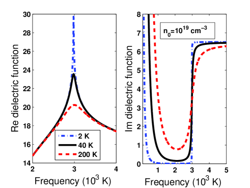
The real and imaginary parts of the dielectric function are plotted in Fig. 1 versus for three values of the collision rate listed in the left panel and the carrier concentration 1019cm-3 which corresponds to the chemical potential K supposed to be much larger than . The electron velocities cm/s and cm/s are known from literature for PbSe, PbTe, and PbS. At low frequencies, , the behavior of the dielectric function is determined by the intraband conductivity. In particular, the imaginary part of the dielectric function grows with the increasing collision rate.
Afterwards, the real part of the dielectric function goes through zero at the frequency determined roughly by the equation
| (8) |
The threshold of absorption (see the right panel) occurs at for the finite carrier concentration. It is smeared while the collision rate (or temperature) is rising. At this frequency, the real part of the dielectric function (left panel) has a peak if the collision rate is low enough. This is an effect of the interband electron transitions.
Finally, we have to consider the case of the empty conduction band when the gap plays a role. Let temperature . The imaginary part, Eq. (5), is given by
which agrees with the known result, Eq. (1), near the band edge, , and goes to the constant value at . We can esimate this constant value using the parameters and listed above. We obtain for all that material in excellent agreement with experimental data KB ; SSA interpolated from frequencies higher than 0.5 eV. To the best of our knowledge, no experimental data exist for frequencies lower than 0.5 eV. Notice that no adjustable parameters are used.
The real part of dielectric function given by the interband transitions in the case is equal
within logarithmic accuracy. Emphasize, that in contrast with the case of degenerate carriers, Eq. (6), the real part of the dielectric function has the large, but convergent value at the band edge . Thus, the contribution into the real part depends on the gap taking the various values in the IV-VI semiconductors. Comparing the values with the constant , we find
We see that the real part of the dielectric function decreases with frequencies in the domain , where the imaginary part has a plateau. Taking the typical size of the gap eV and a reasonable value of the cutoff parameter eV into account, we estimate the maximum value which agrees with the numerical calculations APP .
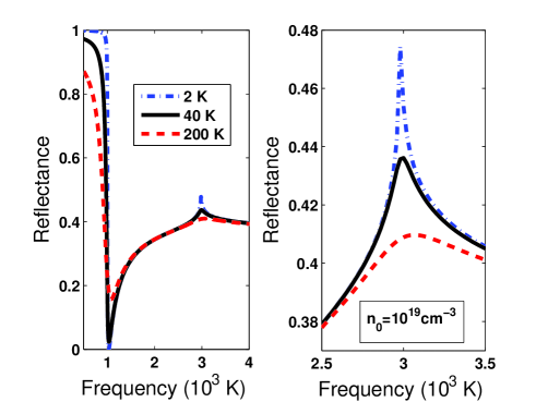
The reflection coefficient
is shown in Fig. 2 for normal incidence, . At low frequencies, the reflection demonstrates the metallic behavior for a sample with carriers. While the frequency increases, reflectance drops to zero at the frequency approximately determined by Eq. (8), where large logarithm due to the interband transitions becomes important. Afterwards, the reflectance is mainly determined by the interband transitions. At the threshold, K, corresponding to the carrier concentration cm-3, the sharp peak of reflectance should be observed for low temperatures (T10 K) and low collision rates (i.e., if the mean free time s for the carrier concentration on the order of 1018–1019 cm-3) due to singular logarithm in the interband conductivity. Observation of the peak presents a characterization of carrier concentration in pure samples. The peak is followed by decreasing reflection because the interband absorbtion grows above the threshold.
In conclusions, we find that the real part of the dielectric function contains a singular contribution from the interband electron transitions. At low frequencies, it gives the large logarithmic term into the dielectric constant. While increasing the frequency, we obtain the dispersion of the dielectric function. Near the threshold of the interband absorption (at for degenerate statistics of carriers), a peak appears at low temperatures if the mean free time of carriers is large enough.
This work was supported by the Russian Foundation for Basic Research (grant No. 07-02-00571).
References
- (1) S.E. Kohn, P.Y. Yu, Y. Petroff, Y.R. Shen, Y. Tsang, and M.L. Cohen, Phys. Rev. B 8, 1477 (1973).
- (2) E.A. Albanesi, E.L. Peltzer y Blanca, A.G. Petukhov, Computation Material Science 32, 85 (2005).
- (3) T.N. Xu, H.Z. Wu, J.X. Si, P.J. McCann, Phys. Rev. B 76, 155328 (2007).
- (4) J.M. An, A. Franceschetti, and A. Zunger, Phys. Rev. B 76, 161310 (2007).
- (5) R. Dalen, in Solid State Physics:Advances in Research and Applications, edited by F. Seitz, D. Turnbull, and H. Ehrenreich (Academic, New York, 1973), Vol.26, p. 179.
- (6) L.A. Falkovsky, A.A. Varlamov, Eur. Phys. J. B 56, 281 (2006).
- (7) D. Korn, R. Braunstein, Phys. Rev. B 5, 4837 (1972).
- (8) N. Suzuki, K. Sawai, S. Adachi, J. Appl. Phys. 77, 1249 (1995).