Quantum effects for ballistic transport in spintronic devices
Abstract
Recent fabrication of atomic precision nanodevices for spintronics greatly boosted their performance and also revealed new interesting features, as oscillating magnetoresistance with number of atomic layers in a multilayered structure. This motivates the need to go beyond the usual theoretical approach of semi-classical continuous layers. Here the simple tight-binding dynamics is used to describe quantum conduction in a multicomponent system with spin-polarized electrodes separated by an ultrathin and atomically coherent non-magnetic spacer (either metallic or insulating). A possibility is indicated for obtaining a huge resonant enhancement of magnetoresistance in such device by a special choice of gate voltage on the spacer element.
pacs:
34.80.Pa; 73.50.-h; 73.61.-r; 75.70.Cn; 85.30.MnI Introduction
In our information based society the development of ultra-high density storage technology is a demanding priority. In this context, the necessity in ultra-high sensitivity read-head devices is a great challenge from both theoretical and experimental points of view. Presently the most promising candidates for this purpose are the magnetic tunnel junctions (MTJ) made by two magnetic electrodes separated by an ultra-thin non-magnetic spacer and their study becomes one of the central topics in the fast developing field of spintronics. Since the early studies by Tedrow and Meservey tedrow1 on spin polarized tunnel conduction, an impressive progress was achieved either in experiment stearns ; meservey ; moodera and in theory buttiker ; schep ; mathon1 for the spintronics applications of this mechanism. The most important recent advances are related to nano-fabrication of multilayered systems on atomic precision level yuasa1 ; parkin , which rises the MTJ performance up to 400 of magnetoresistance and enables a breakthrough to their fundamental quantum properties. It should be noted that the overall number of electronic degrees of freedom in a device like MTJ is macroscopically big which generally suggests a quasi-classical behavior, controlled by the spin-dependent relaxation times or by the spin-dependent tunneling amplitudes. But the essentially quantum behavior turns to be possible at effective separation of a small number (few units) of electronic degrees of freedom among the macroscopically big total number as, e.g., the hoppings between the planes in the spacer among all possible hoppings in a junction, forming a partial quantization of energy spectrum and drastically enhancing the sensitivity of tunnel (or ballistic) transport to external factors sun . Another natural quantization effect is the oscillatory behavior of conductance, either in function of the spacer thickness (or, more exactly, the number of atomic planes) and in electric field on the junction yuasa2 , which may also allow an interesting possibility for specific magnetoconductance oscillations. All this needs that the mode mixing due to the interface roughness and intra-spacer defects be below the characteristic energy quantization scale, and practically requires that the spacer consist of few atomic planes, coherent enough.
Consequently, the theoretical analysis of such systems requires a fully quantum-mechanical description, rather than more traditional semi-classical approaches sim ; julliere . Up to the moment, there already exists a rather well elaborated theoretical base for this description, using the Green function formalism and rigorous ab-initio band calculations butler ; mathon ; mathon2 as inputs to the general Kubo’s formula. However, in many practical cases the direct use of corresponding algorithms leads to heavy enough numerical work, specific for each particular configuration and not very well suited for qualitative predictions and optimization of device performance.
In this paper instead, the simple tight-binding dynamics in single-band approximation is developed, using the straightforward equations of motion for on-site quantum-mechanical amplitudes, to get a handy description of quantum magnetotransport in the ballistic regime (absence of either thermal or impurity scattering) for a trilayer system of spin-polarized electrodes with an ultra-thin and atomically coherent non-magnetic spacer. The motivation for our approach is an easy generalization to more promising device geometries (double barriers or double junctions, etc.) and conduction regimes (including finite electric field effect) which will be presented in a forthcoming work. This presentation is mainly limited to the basics of the method and to its most characteristic results. Thus in Sec. 1 the explicit quantum wave functions are obtained for the -dimensional isolated atomic chain. In the following Sec. 2 the finite D chain is inserted between two D semi-infinite leads and the transmission and reflection coefficients for a collective electronic state are analytically calculated. Further, in Sec. 3 this result is generalized to the -dimensional case and the Landauer conductance formula landauer is used in the D version to yield a clear picture of basic quantum effects evolved in this coherent system. In Sec. 4, the important effects of electronic correlation are included into consideration using the approximation of phenomenological interface potentials, which foresees a more consistent treatment in the spirit of density functional theory. At last, in Sec. 5 a work summary and the principal results are presented and commented.
II 1. Basic chain model
The simplest model for transport over exact electronic states considers a linear chain of identical atoms with single available electronic state on each -th atomic site and describes the single-electron dynamics in the simplest tight-binding approximation with (real) hopping amplitude between nearest neighbor sites (taking the distance between them as unit length).

In this coupled chain, any collective electronic state can be expressed as , with complex amplitudes and atomic states , generated by the second quantization operators acting on the vacuum state . Choosing the on-site atomic energy as a reference (), we write the Hamiltonian operator as:
| (1) |
and obtain the electronic spectrum () as the roots of the secular equation with the corresponding Hamiltonian matrix (where is the Kronecker delta and if , otherwise zero). These determinants satisfy the recurrent relation:
| (2) |
with the initial conditions , that define them exactly through the nd kind Chebyshev polynomials: abramowitz . Then it is convenient to pass to these dimensionless polynomials as functions of the dimensionless variable , rewriting Eq. 2 as:
| (3) |
with . A useful trigonometric parametrization permits to present the general solution of Eq. 3 as:
| (4) |
where . Then the discrete energy spectrum resulting from zeros of is explicitly given by:
| (5) |
Now let be the eigen-vector of the Hamiltonian matrix, Eq. 2, related to the eigen-energy (in what follows we mostly drop the explicit energy arguments of amplitudes like ). Its components satisfy the tight-binding equations of motion
| (6) |
completed by and . Since Eq. 6 for is just equivalent to Eq. 3 for , the eigen-vector components can be written as:
| (7) |
We notice that this solution also satisfies the above mentioned equations of motion for and and provides the "closed" boundary conditions:
| (8) |
As usual, the value of is fixed by the normalization condition, , giving finally the -th component of the eigen-vector (related to the eigen-energy ) as:
Our next purpose is to consider this finite chain inserted into the "circuit" between two semi-infinite chain leads.
III 2. Transmission through discrete chain structure
For a composite system of finite -chain (in what follows called the gate, G) between two semi-infinite chain leads, S (source) and D (drain) (Fig. 2), the tight-binding Hamiltonian, Eq. 1, is extended to: where:
| (9) |
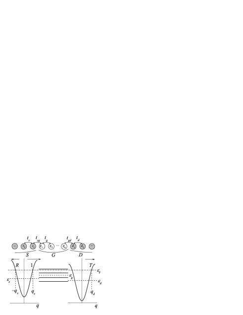
including the respective on-site energies () and hopping parameters (), while the operators , are analogous to , with the formal change of indices . For this macroscopic system, the energy spectrum includes continuous S- and D-bands and possibly discrete G-levels outside these bands. The collective eigen-state for a given energy can be found from the equations of motion that generalize Eq. 6. We denote or the respective local amplitudes of the wave function and define the dimensionless dynamical variables (). Let the S-amplitude be a sum of an incident wave of intensity 1 with the wave number and a reflected wave with certain amplitude and the wave number :
| (10) |
(for regressive order of sites in S), and the D-amplitude present a transmitted wave with certain amplitude and the wave number :
| (11) |
Eqs. 10 and 11 refer to one of fundamental solutions for given (besides that where the incident and reflected waves belong to D and the transmitted one does to S). These forms automatically satisfy the equations of motion within S and D:
| (12) |
(for ), while the pairs of equations on the S/G and G/D interfaces:
| (13) |
and
| (14) |
are the discrete analogs of usual boundary conditions for continuous wave function and its derivative slonczewski . They permit to express the terminal pairs of G-amplitudes through the asymptotic parameters and :
| (15) |
with the interface parameters and . The polynomials are formally the same as given by Eq. 4 with the energy argument . But the energies of our main interest for the transport processes are those close to the Fermi energy which is generally not an eigenvalue, Eq. 5, for the isolated G-element. Therefore the transient "momentum" (not necessarily real) breaks down the closed boundary conditions, Eq. 8, for G and thus enables continuity of quantum states along the composite system. Next, using Eq. 6 for this element in the form:
| (16) |
it is possible to interrelate the terminal G-amplitudes:
| (17) |
Then, Eqs. 15 and 17 yield two independent relations between the coefficients and . Those are readily solved to give:
| (18) |
where the resonance properties result from the denominator:
| (19) |
with the relevant variables as arguments of complex factors and real polynomials , and . Since, in the considered 1D case, all are defined by the single energy variable , the coefficients and can be also defined as functions of energy: and . It is important to notice that the result of Eqs. 18,19 is just analogous to that obtained with the Green function techniques mathon1 , the factors and playing the role of interface Green functions of Ref. mathon1 . A typical behavior of the transmission coefficient is presented in Fig. 3. It shows transmission resonances generated by discrete energy levels of the G-element (by atoms in the chain) as they are passing over the Fermi level within the mutually displaced energy bands. The displacement can be due, for instance, to the Stoner splitting between majority and minority subbands of oppositely polarized S- and D-elements (see also Sec. IV). Notice that the resonances become sharper as the levels approach the band edges, and the maximum transmission in the asymmetric S-D band configuration is not limited to unity. This coefficient enters the Landauer formula landauer for the ballistic conductance through the 1D composite system (in zero temperature limit):

| (20) |
with the Fermi energy . Now, allowing the S and D chains to support spin polarized subbands (where , are the majority and minority spin indices and are the Stoner splitting parameters for ), we can introduce the energy and spin-dependent variables , , for in- and out-channels and obtain from Eq. 20 the spin-dependent conductance values . Finally, the (maximum) magnetoresistance is defined as usually through the difference between the conductance values for parallel and for antiparallel S/D polarization:
| (21) |
Although the state-of-the-art technology already permits development of such genuinely 1D devices agrait and the resonance behavior like that in Fig. 3 (different from the known quantized conductance steps vs voltage bias) can be directly sought in them, it is of major practical importance to generalize the above treatment for a more realistic multilayered structure and this will be done in the next section.
IV 3. 3-dimensional multilayered structure
Passing from 1D composite chain to multilayered (and spin polarized) 3D lattice structure as shown in Fig. 4, we extend the indexing of site operators from and to and , where runs over sites in the th plane and is . Our strategy in this case relies on the conservation of the transversal quasi-momentum in the transitions between the planes mathon ; itoh2 . From the experimental point of view, this requires perfect interfaces that are only reachable with advanced molecular beam epitaxy (MBE) techniques yuasa3 . To describe the situation where is a good quantum number for independent 1D-like longitudinal transport channels, we pass from the site operators to the "planar wave" operators. Thus, for the th plane in the S element, the latter operators are defined as:
| (22) |
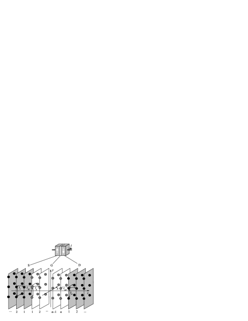
and, similarly, the "planar wave" operators and for D and G elements are written. The related extension of the Hamiltonian is: , where the particular terms are analogous to those in Eq. 9 with the change of all the site operators by the "planar wave" ones and all the on-site energies by the transversal momentum subbands and . The equations of longitudinal motion in terms of the "planar wave" amplitudes , and (for given energy of the collective state) are obtained in analogy with the 1D case. Thus, in the leads S and D (beyond the interfaces, at ), they are analogs to Eq. 12:
| (23) |
| (24) |
with . Also the equations for interface amplitudes:
| (25) |
are analogous to Eqs. 13, 14 and 15. The next derivation, in full similarity with the 1D case, leads to the full dispersion laws in the leads (for ) and to the final conductance formula for particular in-out spin channels:
| (26) |
Here the transmission coefficient depends on the relevant variables and accordingly to: with for and , and the sum in is restricted to the "permitted" range , such that simultaneous equalities are possible for certain real and . In more detail, the latter condition is expressed as:
| (27) |
fully defining the integration procedure (in the limit of continuous ). Then, seeking for optimum performance of the model MR device from Eq. 21, it is of interest to evaluate it as a function of the system parameters, mainly the number of atomic layers in the gate and the on-site energy level of the gate (which can be possibly controlled through the gate bias). Also, variation of the latter parameter from positive to negative values permits to model in our approach the passage from the tunnel magnetoresistance (TMR) to giant magnetoresistance (GMR) regime in a unified way.
The following numerical work can be oriented accordingly to some evident qualitative arguments. The variation of the integrand in Eq. 26 is mainly controlled by that of the polynomials in the denominator of Eq. 19. As seen from the explicit Eq. 4, they are oscillating if (that is, the sampling point in the G-spectrum close enough to the Fermi energy ) and exponentially growing if (remote enough from ). Therefore, the conductance is generally expected to oscillate (either in and in ) as far as the level is close enough to (which can be compared to the GMR regime) and to exponentially decay at far enough from (a generalized TMR regime). The latter decay should asymptotically tend to with at .
In the latter case, the direct calculation by Eqs. 21 may result in and both exponentially small but the latter yet much smaller and thus in (arbitrarily) huge MR values. However, they should not be physically attainable, taking into account that the real multiband electronic structure of transition metals always includes some additional conduction channels, for instance due to the s-bands, whose tunnel contribution slower decays than that of d-bands and is almost spin independent. Therefore it should dominate the transport in the indicated regime and make the real MR exponentially small. A simple phenomenological account of this mechanism in the considered single-band model can be done by introducing a certain spin-independent term into either and values:
| (28) |
to present the MR formula, Eq. 21 as
| (29) |
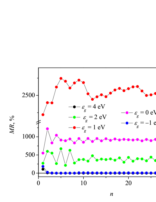

It is just this formula that is used below for all practical MR calculations. Thus, using the band structure parameters: eV, eV, eV and (a reasonable single-band fit for the real Fe band structure, see callaway ; nautial ; mits ) and choosing for simplicity the constant value , we find that the MR behavior vs indeed changes qualitatively at different choices of (Fig. 5). The TMR-like behavior with fast exponential decay appears either at high enough gate level, (which can be compared to a "positive" barrier in the continuum approximation), and at low enough (a "negative" or "hole" barrier), but it develops GMR-like oscillations with greatly increasing overall MR amplitude at the intermediate values (which can be called the "shallow band" regime). The oscillating behavior is in a qualitative agreement with that experimentally observed for MgO moderate tunnel barriers between Fe electrodes yuasa1 , except for stronger first oscillations than in the data. However, it will be shown below that these strong oscillations are effectively moderated when taking into account the specific interface effects between metal and insulator layers. The most notable feature of the calculated MR is its amazingly high maximum value, of the order of 3000 %, indicating a huge potentiality of the quantum coherent conduction regime.
For the same choice of parameters, the calculated dependencies of MR vs (at fixed values of ) are shown in Fig.6. In concordance with the above considered behavior, they practically vanish beyond the range of intermediate and display a finite number of resonance peaks within this range (reminiscent of 1D resonances in Fig. 3), reaching the same highest order of magnitude in the "shallow band" regime. These very high values in the present tight-binding approach contrast with the known result for the model of almost free electrons on the continuous rectangular barrier slonczewski , where MR reaches zero minimum at low barrier height. As yet, the dependence was only studied experimentally for Al-O spacers tezuka , possessing most probably polycrystalline or amorphous structure and high enough , so it could be of interest to try it also with epitaxial MgO spacers and possibly with those spacer materials that can realize the "shallow band" condition.
V 4. Interfacial Effects
In this section, we will discuss the interfacial effects present at the metal/insulator or metal/non-magnetic-spacer interfaces. This is motivated by the analogy with the well known case of Schottky barrier at metal/semiconductor interfaces, leading to such interesting physical effects as band bending sze . It is known from X-ray and ultraviolet photoemission spectroscopy (XPS and UPS) that some charge transfer effects also appear at the metal-insulator interface, leading to formation of an interfacial charge-dipole whose magnitude is defined by the localized states at interfaces popinciuc . Since this dipole directly affects the efficiency of tunneling, it is also important to evaluate its effect in the magnetoresistance.
The best treatment of this problem is to introduce self-consistently a charging energy (, commonly called the built-up voltage) due to a charge accumulation in the framework of the density functional theory (DFT). This is going to be done in the future work, but at the moment we will develop simple analytic formulas to take into account these interfacial effects qualitatively. Despite of its simplicity, the model can exemplify in which way the formation of charge dipoles affects the magnetoresistance ratio.

We go on using the same model of Sec. IV but considering extra charge energies on the sites pertaining to the two atomic planes on both sides of each interface (see Fig. 7) as an approximation for more realistic charge and potential distributions around interfaces, obtained by numerical DFT calculations butler . The -perturbation results in new boundary conditions and, as a consequence, in a new transmission coefficient. In this approximation, there is no changes in equations of motion within the particular elements (S, D and G), but new pairs of equations appear at the S/G and G/D interfaces, involving the charge energy :
| (30) |
These boundary conditions allow to re-calculate two terminal G-amplitudes in function of the parameters . Interconnecting these terminal amplitudes leads to the transmission formula, Eq. 18, but with the modified denominator where:
| (31) |
It is easy to see that in the limit of .
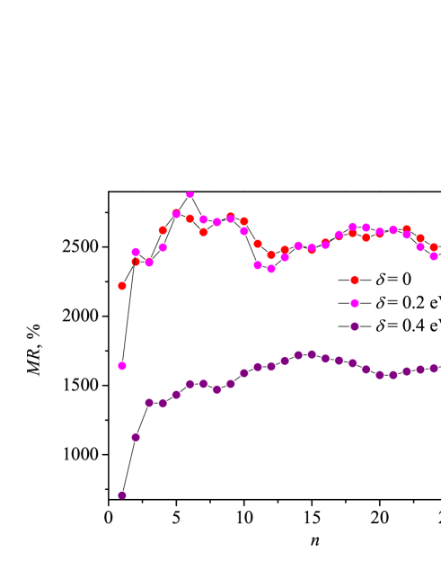
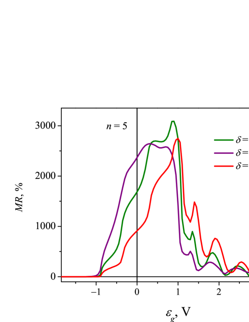
The MR defined from Eqs. 29,31 in function of the number of gate atomic planes and of the gate voltage for tree values of the interface potential are presented in Figs. 9, 9. The obtained softening of first oscillations makes these curves more similar to the experimental observations yuasa1 . An unexpected result is that the effect of an extra barrier due to the charge energy can yet reinforce the calculated MR peak in the shallow band regime, though reducing the values in the TMR regime at higher barrier height. Obviously, the charge energy barrier reduces the conductance (either in P and AP configurations), but the MR enhancement is mainly due to a much stronger reduction of the AP conductance. Apparently it results from the wave function localization caused by coherent resonances in the interfacial potential wells. This idea of charge energy induced resonances is corroborated by the calculated sharpening of peaks just in the AP conductance. Amazingly high peak MR values, reaching for a reasonable choice of eV (similar to the numerical estimate for Fe-MgO interfaces, butler ), should motivate fabrication of new devices with the choice of such spacer materials as semiconducting (Ge, Si) or semimetalic (Sb, As). Though the peak value may be obviously decreased under the effects of electron-electron, electron-phonon, and electron-magnon interactions, finite temperature and disorder, it expresses one of the principal results of this work, demonstrating that the highest possible MR value should be reached in the shallow-band regime for non-magnetic spacer by adjusting to the strongest resonance condition, once electronic coherence is assured.
VI 5. Conclusions
In this work a theoretical approach was developed to fully coherent spin-dependent quantum transport in nanolayered magnetic junctions, using single-band tight-binding model with explicit equations of motion for wave-function amplitudes. The analytic solutions for the transmission and reflection coefficients were generalized for a 3-dimensional magnetic junction structure. The simple zero temperature calculations have revealed the most pronounced enhancement of the magnetoresistance in the "shallow band" regime, defined by low gate voltages (Fig. 6). Another important feature for this gate voltage regime is the calculated oscillatory behavior of MR with the number of atomic planes in the spacer. In support of these theoretical predictions, the calculations also reveal that the oscillatory regime starts already at moderate gate voltages, eV. This agrees rather well with the experimental observation by Yuasa yuasa1 of clear MR oscillations at low enough gate voltage barrier eV in a Co/MgO/Co structure. So it is concluded that the best MR values for a quantum magnetic junction could be reached using shallow band materials for spacer layers, the possible candidates sought between transition metals (Cr greullet in junctions of the type Fe/Cr/Fe or Zn in junctions of the type Co/Zn/Co), semiconductors (Ge, Si), or semimetals (Sb, As). Finally, the important effect of charge build-up (Sec. V) on the junction interface was also considered and, though in a simple phenomenological approach, a possibility is shown for even stronger enhancement of the magnetoresistance in presence of the extra charge-energy for the same shallow band regime, emphasizing again the promise of using the low -materials. To verify these model predictions, the future work must include various realistic effects, such as those of finite temperature and self-consistent density functional theory (DFT), to adopt also the multiband electronic structure, spin-transfer processes, and non-linear conduction.
VII Acknowledgements
The authors wish to thank J.B. Sousa, P.P. Freitas, J. Lopes dos Santos, J. P. Araújo and H. L. Gomes for their helpful discussions and friendly support of various aspects of this study. The work was partially supported by Portuguese Foundation of Science and Technology, FCT, through the grant SFRH/BD/24190/2005 (H. S.).
References
- (1) P. M. Tedrow and R. Meservey, Phys. Rev. Lett. 26, 192 (1971).
- (2) M. B. Stearns, J. Magn. Magn. Mater 5, 167 (1977).
- (3) R. Meservey, J. Appl. Phys. 49, 1405 (1978).
- (4) J. S. Moodera, L. R. Kinder, T. M. Wong, and R. Meservey, Phys. Rev. Lett. 74, 3273 (1995).
- (5) M. Büttiker, Phys. Rev. B, 27, 6178 (1983)
- (6) K. M. Schep, P. J. Kelly, and G. E. W. Bauer, Phys. Rev. Lett. 74, 586 (1995).
- (7) J. Mathon, A. Umerski, and M. Villeret, Phys. Rev. B 55, 14378 (1997).
- (8) S. Yuasa, T. Nagahama, A. Fukushima, Y. Suzuki and K. Ando, Nature Materials, 3, 868 (2004).
- (9) S. S. P. Parkin, C. Kaiser, A. Panchula, P. M. Rice, B. Hughes, M. Samant, and S.-H. Yang, Nature Materials, 3, 862 (2004).
- (10) J. J. Sun, R. C. Sousa, T.T.P. Galvão, V. Soares and P. P. Freitas. J. Magn. Soc. Japan 23, 55 (1999).
- (11) S. Yuasa, T. Nagahama, T. Kawakami, K. Ando, and Y. Suzuki, J. Phys. D: Appl. Phys. 35, 2427 (2002).
- (12) J. G. Simmons, J. Appl. Phys. 34, 1793 (1963).
- (13) M. Julliere, Phys. Lett. A 54, 225 (1975).
- (14) W. H. Butler, X.-G. Zhang, T. C. Schulthess, and J. M. MacLaren, Phys. Rev. B 63, 054416 (2001).
- (15) J. Mathon, M. Villeret, and H. Itoh, Phys. Rev. B 52, R6983 (1995).
- (16) J. Mathon and A. Umerski, Phys. Rev. B 63, 220403 (2001).
- (17) R. Landauer, IBM J. Res. Dev., 1, 223 (1957).
- (18) Abramowitz, M. and Stegun, I. A. (Eds.). Handbook of Mathematical Functions with Formulas, Graphs, and Mathematical Tables, 9th printing. New York: Dover, 1972.
- (19) N. Agraït, A. Levy Yeyati, J.M. van Ruitenbeeck, Phys. Rep. 377, 81 (2003).
- (20) J. C. Slonczewski, Phys. Rev. B 39, 6995 (1989).
- (21) H. Itoh, J. Phys. D: Appl. Phys. 40, 1228 (2007).
- (22) S. Yuasa, A. Fukushima, H. Kubota, Y. Suzuki, and K. Ando, Appl. Phys. Lett. 89, 042505 (2006).
- (23) J. Callaway and S. W. Wang, Phys. Rev. B 16, 2095 (1977).
- (24) T. Nautial and S. Auluck, Phys. Rev. B 34, 2299 (1986).
- (25) On-line database of electronic structures available at https://caldb.nims.go.jp/
- (26) N. Tezuka and T. J. Miyazaki, J. Magn. Magn. Mater. 177-181, Part 2, 1283 (1998).
- (27) S. M. Sze, Physics of Semiconctor Device, John Wiley & Sons, Inc., 1981.
- (28) M. Popinciuc, H. T. Jonkman, and B. J. van Wees, Journal of Appl. Phys. 101, 093701 (2007)
- (29) J. S. Moodera, J. Nowak, L. R. Kinder, P. M. Tedrow, R. J. M. van de Veerdonk, B. A. Smits, M. van Kampen, H. J. M. Swagten, and W. J. M. de Jonge, Phys. Rev. Lett. 83, 3029 (1999).
- (30) J. S. Moodera and J. Mathon, J. Magn. Magn. Mater 200, 248-273 (1999).
- (31) F. Greullet, C. Tiusan, F. Montaigne, M. Hehn, D. Halley, O. Bengone, M. Bowen, and W. Weber, Phys. Rev. Lett. 99, 187202 (2007).