Tunneling conductance of a two-dimensional electron gas with Rashba spin-orbit coupling
Abstract
We theoretically studied the in-plane tunneling spectroscopy of the hybrid structure composed of a metal and two-dimensional electron gas with Rashba spin-orbit coupling. We found that the energy spacing between two distinct features in the conductance spectrum can be used to measure the Rashba energy. We also considered the effect that varying the probability of spin-conserving and spin-flip scattering at the interface has on the overall conductance. Surprisingly, an increase in interface scattering probability can actually result in increased conductance under certain conditions. Particularly, in the tunneling regime, an increase in spin-flip scattering probability enhances the conductance. It is also found that the interfacial scattering greatly affects the spin polarization of the conductance in metal, but hardly affects that in the Rashba system.
pacs:
73.40.Ns, 73.40.Gk, 73.23.-b, 72.25.Dc, 72.25.MkI Introduction
Structural inversion asymmetry of the confining electrostatic potential results in an intrinsic spin-orbit coupling of electrons in a two-dimensional (2D) electron gas (EG), which can be described by the Rashba Hamiltonian rashba ; rashba2 ; rashba3 :
| (1) |
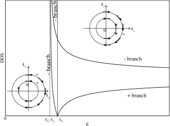
where is 2D momentum, is the electron effective mass, is the direction perpendicular to the plane of motion, is the spin-orbit coupling parameter, which can be tuned by applying an external gate voltage perpendicular to the 2D plane, and the components of are the Pauli spin matrices. The spin-orbit interaction lifts the spin degeneracy and causes the original parabolic energy spectrum to split into two branches: , where is the magnitude of the wave vector. The density of states of this system is the same as that of the 2D free electron gas for all energies higher than the crossing point of the two branches. However, at the bottom of the band, the density of states has van Hove singularity because the minus branch has an annular minimum for instead of a single-point minimum as in the free electron gas. These properties lead to interesting phenomena, like the spin hall effect (see e.g. Refs. engel for review), and to applications in spintronics (see e.g. Refs. zutic for review).
The Rashba effect has been seen in many systems like surface alloys and semiconductor heterostructures. Several techniques have been used to study the spin-split states in these systems. For instance, angle-resolved photoemission spectroscopy lashell ; rein ; henk ; cer ; popovic and scanning tunneling microscopy ast are used in surface alloys. The former technique is utilized mainly to obtain the energy dispersion and the Fermi surface map, from which the effective mass, the magnitude of the band splitting, and hence the Rashba spin-orbit coupling energy, , can be extracted lashell ; rein ; henk ; cer ; popovic . In the latter technique, the electric current is driven through a sharp tip perpendicular to the 2D plane and the differential conductance () spectrum can be obtained. One can deduce the Rashba energy by fitting the spectrum to the local density of states of the 2DEG ast . In both cases, to obtain information about the Rashba spin-orbit coupling, extensive data fitting is needed.
In semiconductor heterostructures, the Rashba energy is measured using the Shubnikov-de Haas oscillations nitta ; engels . The existence of the spin splitting at the Fermi energy leads to beating in the oscillations and the Rashba energy can be deduced from the position of the beating node. However, because this technique is done in the presence of magnetic field, it tends to provide an overestimate of the Rashba energy because it includes the effect of the Zeeman spin splitting lommer .
In this article, we propose a way to measure the spin-splitting energy more directly from the experimental data: the in-plane tunneling spectroscopy. In this technique, the Rashba energy can be determined by the energy difference between two features in the conductance spectrum. The required condition for the measurement is that the energy resolution of the tunneling spectra is at least of the order of the Rashba energy itself. This condition can be easily achieved in modern tunneling measurements wolf .
An intriguing property of 2DEG with Rashba spin-orbit interaction is spin-dependent transport. Many theoretical investigations have shown that both electric and spin transport in hybrid structures between the Rashba system and various materials, like metals liu ; lee ; mari , ferromagnets mari ; hu2 ; hu ; jiang , and superconductors tanaka , are affected by the strength of the spin-orbit coupling liu ; lee ; mari ; hu2 ; hu ; jiang ; tanaka , the inequality of the effective masses liu ; lee ; hu ; jiang , and the transparency of the interface hu2 ; hu ; tanaka . However, in these previous studies, only spin-conserving interfacial scattering was considered. In the presence of interfacial spin-flip scattering, the equations describing the spin-up and spin-down spin states are coupled and one expects interesting consequences of this. For instance, in the study of the tunneling conductance spectrum of a semiconductor/superconductor junction zutic2 , the non-spin-flip scattering, when present alone, is found to suppress the Andreev reflection process and hence the subgap conductance as expected. However, when the spin-flip potential scattering is also present at the interface, their combined effect surprisingly enhances the subgap conductance zutic2 .
Here, we consider how the scattering potential barrier affects both the conductance spectrum and the spin polarization of the conductance of a junction consisting of a metal and a Rashba system. As in previous work by Zutic and Das Sarma zutic2 , we find that the conductance spectrum, which is usually suppressed in the presence of the interfacial scattering, can be enhanced by the combined effect of both types of scattering. We also find that the spin polarizations of conductance of the metal and the Rashba system are not equal. The spin polarization in the latter depends weakly on interfacial scattering, while that in the former is greatly affected. This suggests that a spin imbalance in the Rashba system is robust against variation in the quality of the junction interface.
In the next section, we describe the theoretical method and assumptions. In Section III, we provide the results and discussion. The conclusion is given in the last section.
II Method of calculation and assumptions

We represent our junction by an infinite 2D system which lies on plane, where the metal and the Rashba system occupy the and region respectively. The two regions are separated by a flat interface at . The interfacial scattering is modeled by a Dirac delta function potential btk . We consider ballistic transport in our junction. In the one-band effective-mass approximation, we describe our system by the following Hamiltonian:
| (2) |
Each term is the matrix acting on spinor states. . The effective mass is position-dependent, i. e., , where and are effective electron masses in the metal and the Rashba system respectively, and is the Heaviside step function. is also a position-dependent function and is modeled by the expression
| (3) |
where represents the scattering potential at the interface, is the energy difference between the Fermi level and the bottom of the plus branch (see FIG. 1), and is the Fermi energy of the metal. We assume that is much larger than . The diagonal elements of , and correspond to the non-spin-flip scattering potential characterizing the quality of the junction, while describe spin-flip scattering zutic2 . The Rashba Hamiltonian is written as zulicke
| (4) |
where .
From the Hamiltonian, one can obtain the eigenstates and eigenenergy for the electrons in each region as follows. In the region, the energy spectrum is
| (5) |
where is the magnitude of the 2D momentum of the electrons. In the region, the eigenenergy is obtained as
| (6) |
where is the magnitude of the 2D momentum and . FIG. 1 shows the energy spectra and energy contours of the excitations in both sides of the junction.
The wave function of the electrons in metal is written as a linear combination of incoming momentum state with equal spin components and a reflected state of the same energy and :
| (7) |
where the are the amplitudes for reflection of spin-up and spin-down electrons respectively. and , where is the angle between and the axis. The magnitude of the momentum, , depends on energy as
| (8) |
Similarly, in the Rashba system, the wave function is obtained as a linear combination of two outgoing eigenstates of the same energy and :
| (9) |
where are the angles between and the axis. For , and are the transmission amplitudes of electrons to plus and minus branch respectively. When , and refer to the transmission amplitudes of electrons to states with smaller and larger of the minus branch respectively. The upper and lower signs in the first term of Eq. (9) are for and respectively. and , where the magnitudes of the momenta, , depend on energy as
| (10) | |||||
| (11) |
Again, in Eq. (11) the upper and lower signs are for and respectively. The relationship between the angles and is
| (12) |
We can obtain the probability amplitudes and from the following matching conditions that ensure probability conservation zulicke .
| (13) | |||||
| (14) |
where . The diagonal elements of will henceforth be referred to as and , while the off-diagonal element will be denoted by . In what follows the spin flip term will be responsible for the enhancement of a feature at the branch-crossing point in the conductance spectrum.
The particle current density along the direction is obtained from
| (15) |
where is the spinor wave function, and . From the current density, the reflection and transmission probabilities can be obtained:
| (16) | |||||
| (17) | |||||
| (18) | |||||
| (19) |
where are the reflection probabilities to spin-up and spin-down states, and are the corresponding transmission probabilities. Also, the upper and lower signs in are for and respectively. As mentioned earlier, the matching conditions ensure that .
Since the current is independent of , we consider the current density in the metal for simplicity. It can be written as a function of applied voltage as follows.
| (20) |
where is the electron charge, is the component of the electron group velocity, and is Fermi distribution function.
By changing the integration variable and setting temperature to zero for simplicity, one can obtain the expression for the electric current as
| (21) |
where is the area of the metal and is the maximum angle of the incident electrons from the metal (see FIG. 1): . Thus, the differential conductance at zero temperature is
| (22) |
The finite temperature will smear the features in the conductance spectrum but will not change their positions (assuming that the strength of the Rashba spin-orbit coupling does not depend on temperature).
The spin polarization of the conductance is defined as
| (23) |
where is the number of electrons with spin that cross a plane of interest per unit time. In terms of the reflection probabilites this spin polarization in the metal can be written as
| (24) |
and the spin polarization in the Rashba system in terms of the transmission probabilities is written as
| (25) |
As expected, the spin polarization measures the difference in number of the carriers with spin-up and spin-down on each side.
III Results and discussion
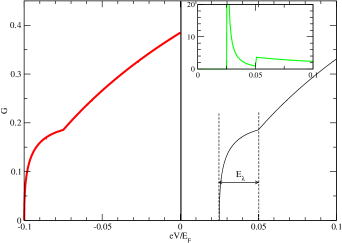
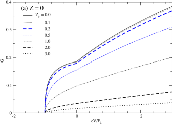
In this section, we discuss the effect of the interfacial scattering on the differential conductance spectra and the spin polarization of conductance on each side of the junction. In all plots, we set and , which corresponds to typical experimental values in metal/Rashba system junctions zutic2 ; koga . In FIG. 2, two conductance plots for two values of are shown. Positives values of means the energy spectrum of the Rashba system is unoccupied and the positive across the junction will cause the current to flow from the metal to the Rashba system.
In the case shown in FIG. 2 where the energy spectrum is occupied (), the results are identical in shape to those in the unoccupied case (), but the applied voltage across the junction has to be negative. There are two main features at the voltage corresponding to the bottom and the branch-crossing of the energy band. The distance between them depends on , which is the quantity of interest. The value of is not important, i. e., changing causes a rigid shift in energy, and will henceforth be set equal to zero.
We do not consider the spin filtering interface. That is, we set the non-spin-flip scattering strength . It is well-known that the difference in and will cause a spin-filtering effect. That is, a higher will make the transport of the spin-up electrons less favorable and vice versa. This effect cannot be seen in the conductance spectrum and will not be considered in the spin polarization.
III.1 Differential conductance spectra
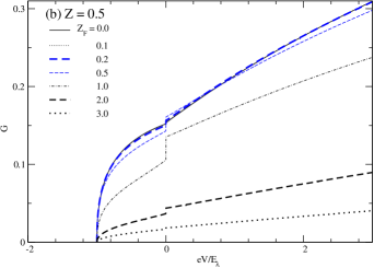
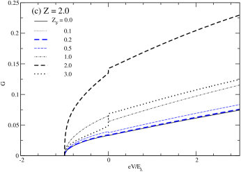
In all conductance plots, the conductance is in units of . The conductance spectra with different in different limits of are shown in FIG. 3. Junctions with metallic contacts are characterized by , whereas those in the tunneling limit are characterized by . In general, the conductance is zero until the applied voltage reaches , which is the bottom of the band of the Rashba system. The conductance increases suddenly with large initial slope that decreases steadily until a second feature: the kink occurring at , which is the crossing point of the two branches of the band. After this point, the conductance increases approximately linearly. In the presence of , there occurs a discontinuity in the conductance at . The height of the jump depends on both and . The energy difference between the onset and the discontinuity in slope of the conductance spectrum can be used to measure the magnitude of the Rashba energy .
In addition to the influence on the discontinuity at , the interfacial scattering affects the overall conductance spectrum as well. For metallic contacts, the spin-flip scattering suppresses the conductance as expected. However, in the intermediate and the tunneling limits, the results are rather surprising. As can be seen in FIG. 3(b) when , the increase in from zero to a small value (less than 0.5) does not affect the conductance much. Only when is increased beyond 0.5, does the conductance get suppressed. When is high, e. g. as in FIG. 3(c), the conductance spectrum can be enhanced by the increase in up to a value , after which the spectrum becomes suppressed. is found to depend strongly on .
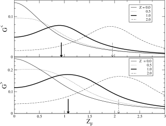
One can see the effect on the conductance spectrum of spin-flip scattering more clearly by considering plots of the conductance as a function of for energies just below and just above . In FIG. 4, and , where , are plotted as a function of for different values of . For small , both and decrease with as expected. However, this trend starts to change when is higher than 0.5. That is, both and increase with and reach a maximum value at (as indicated by arrows in FIG. 4), after which they decreases with . Notice that is a little smaller for than for and is approximately equal to . It should be noted that a similar dependence of both and on can also be seen, if one plots and as a function of instead.
III.2 Spin polarization of conductance
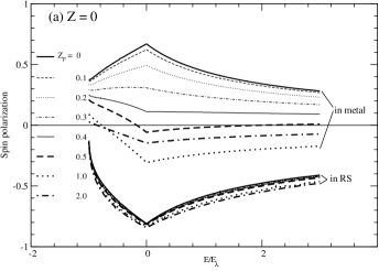
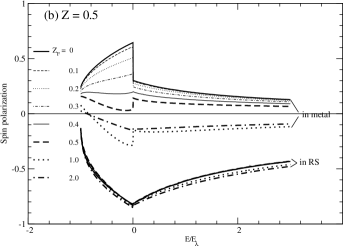
The plots of the spin polarizations in both metal and Rashba system as a function of energy are shown in FIG. 5. The spin polarizations of the two sides are very different. In Rashba system, it is always negative, whereas in the metal it is positive when the spin-flip scattering is not strong. This may be understood by considering the density of states of the Rashba system.
The density of states of the minus branch is larger than that of the plus branch. As we can see from FIG. 6, because the spins of the transmitted states of the minus branch are mostly pointing down, it is not surprising that the spin polarization in the Rashba system is negative. As for the metal side, because more spin-down states are transmitted into the Rashba system, the spin polarization is positive.
The interfacial scattering does not affect the spin polarization in the Rashba system as much as in the metal. The increase in either or seems to slightly change the magnitude of the spin polarization. However, in metal the interfacial scattering potential affects the spin polarization a great deal. For a particular value of , the increase in can cause the spin polarization in metal to change sign.
IV Conclusions
According to the results from our simple model, one can directly use in-plane tunneling conductance spectrum to measure the Rashba energy of a system with the Rashba spin-orbit coupling. The energy difference between the onset and the discontinuity in slope of the conductance spectrum is equal to the Rashba energy. Both features are found to be robust against variation in the quality of the junction.
Experimentally, to be able to measure the Rashba energy, the required energy resolution is at least of the order of the Rashba energy itself and the temperature is low enough in order that both features are visible. The Rashba energies in semiconductor-based heterostructures such as InAs, InGaAs and GaN, are of order 1 meV sasa ; grundler ; matsu ; koga2 ; fuji ; ikai , whereas those of surface alloys like Li/W(110), Pb/Ag(111), and Bi/Ag(111) can be as large as 200 meV ast ; roten ; pacile ; ast2 . These conditions can be readily met in modern tunneling measurements wolf .
We also found that as the current is driven through the system, an imbalance of spin in both sides occurs. The spin polarization of the conductance in the metal is found to depend strongly on both types of the interfacial scattering and can disappear when the barrier is in the tunneling regimes. On the contrary, in the Rashba system the spin polarization is always present and only slightly affected by interfacial scattering. This finding suggests that the spin imbalance caused by current flow in the system with the Rashba spin-orbit coupling is robust against variation in the quality of the junction as well.
Acknowledgements.
We thank Dr. Michael F. Smith for critical reading of the manuscript. Also, we would like to acknowledge financial support from Cooperative Research Network (Physics). P.P. thanks Thai Research Fund and Commission on Higher Education, Thailand (grant no. RMU488012 and CHE-RES-RG ”Theoretical Physics”) for financial support. M.B. was supported by the Research Corporation, CIFAR and NSERC.References
- (1) E. I. Rashba, Sov. Phys. Solid State 2, 1109 (1960).
- (2) Y. A. Bychkov and E. I. Rashba, J. Phys. C 17, 6039 (1984).
- (3) Y. A. Bychkov and E. I. Rashba, JETP Lett. 39, 78 (1984).
- (4) H. Engel, E. I. Rashba, and B. I. Halperin, Handbook of Magnetism and Advanced Magnetic Materials (Chichester: John Wiley and Sons Limited, 2007).
- (5) I. Zutic, J. Fabian, and S. Das Sarma, Rev. Mod. Phys. 76, 323 (2004).
- (6) S. LaShell, B. A. McDougall, and E. Jensen, Phys. Rev. Lett. 77, 3419 (1996).
- (7) F. Reinert, J. Phys.: Condens. Matter 15, S693 (2003).
- (8) J. Henk, M. Hoesch, J. Osterwalder, A. Ernst, and P. Bruno, J. Phys.: Condens. Matter 16, 7581 (2004).
- (9) H. Cercellier, Y. Fagot-Revurat, B. Kierren, F. Reinert, D. Popović, D. and Malterre, Phys. Rev. B 70, 193412 (2004).
- (10) D. Popović,F. Reinert, S. Hüfner, V. G. Grigoryan, M. Springborg, H. Cercellier, Y. Fagot-Revurat, B. Kierren, and D. Malterre, Phys. Rev. B 72, 045419 (2005).
- (11) C. R. Ast, G. Wittich, P. Wahl, R. Vogelgesang, D. Pacilé, M. C. Falub, L. Moreschini, M. Papagno, M. Grioni, and K. Kern, Phys. Rev. B 75, R201401 (2007).
- (12) J. Nitta, T. Akazaki, H. Takayanagi, and T. Enoki, Phys. Rev. Lett. 78, 1335 (1997).
- (13) G. Engels, J. Lange, Th. Schäpers, H. and Lüth H, Phys. Rev. B 55, R1958 (1997).
- (14) G. Lommer, F. Malcher, and U. Rössler, Phys. Rev. Lett. 60, 728 (1988).
- (15) E. L. Wolf, Principles of tunneling spectroscopy (Oxford University Press, New York, 1989).
- (16) G. Liu and G. Zhou, Chin. Phys. Lett. 22, 3159 (2005).
- (17) M. Lee and M. Choi, Phys. Rev. B 71, 153306 (2005).
- (18) V. M. Ramaglia, D. Bercioux, V. Cataudella, G. De Filippis, C. A. Perroni, and F. Ventriglia, Eur. Phys. J. B 19, 365 (2003).
- (19) C. M. Hu and T. Matsuyama, Phys. Rev. Lett. 87, 066803 (2001).
- (20) T. Matsuyama, C. M. Hu, M. Grundler, G. Meier, and U. Merkt, Phys. Rev. B 65, 153322 (2005).
- (21) Y. Jiang and M. B. A. Jalil, J. Phys.: Condens. Matter 15, L31 (2003).
- (22) T. Yokoyama, Y. Tanaka, and J. Inoue, Phys. Rev. B 74, 035318 (2006).
- (23) I. Zutic and S. Das Sarma, Phys. Rev. B 60, R16322 (1999).
- (24) G. E. Blonder, M. Tinkham, and T. M. Klapwijk, Phys. Rev. B 25, 4515 (1982).
- (25) U. Zülicke and C. Schroll, Phys. Rev. Lett. 88, 029701 (2002).
- (26) T. Koga, J. Nitta, H. Taganayagi, and S. Datta, Phys. Rev. Lett. 88, 126601 (2002).
- (27) S. Sasa, K. Anjiki, T. Yamaguchi, and M. Inoue, Physica B 272, 149 (1999).
- (28) D. Grundler, Phys. Rev. Lett. 26, 6074 (2000).
- (29) T. Matsuyama, R. Kürsten, C. Meibner, and U. Merk, Phys. Rev. B 61, 15588 (2000).
- (30) T. Koga, J. Nitta, T. Akazaki, and H. Takayanagi, Phys. Rev. Lett. 89, 046801 (2002).
- (31) K. Fujii, Y. Morikami, T. Ohyama, S. Gozu, and S. Yamada, Physica E 12, 434 (2002).
- (32) L. Ikai, J. K. Tsai, W. J. Yao, P. C. Ho, L. W. Tu, T. C. Chang, S. Elhamri, W. C. Mitchel, K. Y. Hsieh, J. H. Huang, H. L. Huang, and W. C. Tsai, Phys. Rev. B 65, 161306 (2002).
- (33) E. Rotenberg, J. W. Chung, and S. D. Kevan, Phys. Rev. Lett. 82, 4066 (1999).
- (34) D. Pacilé, C. R. Ast, M. Papagno, C. Da Silva, L. Moreschini, M. Falub, A. P. Seitsonen, and M. Grioni, Phys. Rev. B 73, 245429 (2006).
- (35) C. R. Ast, J. Henk, A. Ernst, L. Moreschini, M. C. Falub, D. Pacilé, P. Bruno, K. Kern, and M Grioni, Phys. Rev. Lett. 98, 186807 (2007).