On the calculation of Schottky contact resistivity
Abstract
This numerical study examines the importance of self-consistently accounting for transport and electrostatics in the calculaiton of semiconductor/metal Schottky contact resistivity. It is shown that ignoring such self-consistency results in significant under-estimation of the contact resistivity. An explicit numerical method has also been proposed to efficiently improve contact resistivity calculations.
I Introduction
In modern MOSFET designs, silicon/silicide Schottky hetero-interfaces are commonly used to form source/drain contacts. As the device size continues to shrink with each generation, the resistance associated with the silicon/silicide contacts begins to have its impact on the device performance [1]. Therefore, it becomes important to achieve an accurate yet efficient method to evaluate silicon/silicide contact resistivity at different doping concentrations and temperatures. Some widely refered earlier work on J-V relation and contact resistance of Schottky contact are due to [2, 3, 4]. They identified three regimes where the major current contribution comes from field emission, thermionic field emission or thermionic emission, depending on doping concentration and temperature. Analytical expressions of contact resistivity were obtained for each of the three regimes. However, their works were based on two assumptions. Firstly, Poisson equation was only solved by assuming fully depletion of free carriers within the depletion region, i.e. the band-bending of silicon near the interface is parabolic. Secondly, the continuity equation was not solved, and therefore the carrier quasi-Fermi level was assumed to be flat across the depletion region. To examine the validity of those two assumptions, we have implemented in our device simulator Prophet a self-consistent Schottky barrier diode simulation model proposed by [5]. In this physical model, Poisson and continuity equations are simultaneously solved with the distributed tunneling current self-consistently included. By comparing analytical models against this physical model, we are able to demonstrate that those two assumptions lead to significant deviation in contact resistivity calculations, particularly at high doping concentration of modern device and high temperature under ESD condition. In this work, we also extend the analytical model by removing those two assumptions. In the improved model, a unified contact resistance expression is explicitly obtained111Numerical integrations are involved in the expression., and the results show excellent match with those from the physical model.
II Models and Results
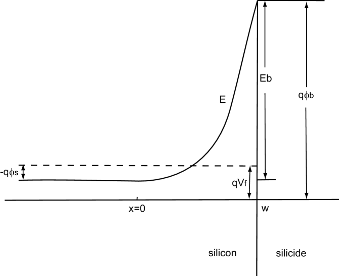
In Fig.1 is a schematic energy band-diagram of a silicon/silicide Schottky contact. In this work, we assume the majority carriers are electrons. The hetero-interface in this plot is at location and the depletion region is between and . The difference of silicon/silicide affinity is where is the elementary charge. The doping density in silicon region is and the effective density of states is . The difference between conduction band and quasi-fermi level at charge neutral region is . The applied forward bias is . If we only consider the contact resistance at very low bias, we have . The barrier height can be expressed as . We base this work on Maxwell-Boltzmann statistics for mathematical simplicity 222Also because the physical model is currently implemented based on M-B statistics.. All the derivations below can be readily extended to Fermi-Dirac statistics, and the effects investigated in this work should still be present in that case. It can be shown that under M-B statistics.
Following the treatment of [6, 7], the general tunneling probability at loaction within the depletion region is given by
| (1) | |||||
where is the tunneling effective mass, is the conduction bandedge energy at position . The electro-static potential is given by . It can be seen that, if is known, the tunneling probability can be evaluated explicitly by performing the numerical integral in Eqn. 1. Since the bandedge energy is a monotonic function of position , it is convenient to use a dimensionless quantity as the basic variable [3]. In doing so, the general expression for the tunneling probability is re-written as
| (2) |
where . The function carries the information of potential variation in the depletion region and is defined as
| (3) |
In the literatures, different energy band-diagrams () have been assumed to calculate . In the work of [3], they based their calculation completely on the parabolic band-bending relation
| (4) |
and obtained an analytical expression
| (5) |
where . However, the work in [2, 5] was based on another widely used formular for tunneling probability:
| (6) |
where is the electrical field perpendicular to the interface. Matsuzawa et al. used in their work [5], and therefore the tunneling probability can be re-written as
| (7) |
This expression can also be directly derived from the general expression (Eqn. 1) by assuming linear relation between and . It should be noted that although triangular potential barrier was assumed in obtaining Eqn. 7, the position appears explicitly in the formula, which still contains the band-bending information. In our physical model, the treatment follows that of [5], and Eqn. 7 is adopted. In the simulation, the realistic potential variation enters through the relation of by solving the Poisson and continuity equations. In order to have fair comparisons between numerical models and the physical model, we use Eqn. 7 for the numerical models in most cases throughout this work.
The general expression for the forward current density (electrons inject from silicon to silicide) is given by
| (8) |
where for Richardson constant , is the local electron quasi-Fermi level variation compared with that at charge neutral region. Therefore, if constant quasi-Fermi level is assumed, is always zero within the entire silicon region. The first term in the bracket of Eqn. 8 corresponds to field emission and thermionic field emission, while the second term is from the thermionic emission. Similarly, the reverse current density (electron inject from silicide to silicon) is given by
| (9) |
The total net current density as a function of is therefore obtained as
| (10) | |||||
where is the value of at the interface. The contact resistivity at zero bias is then obtained as [4]. In previous work [2, 3], continuity equation was not solved. Therefore, the variation of within the depletion region was ignored. Under such an assumption, the total current density is obtained as
| (11) |
Hence, the inverse of contact resistivity at zero bias is
| (12) | |||||
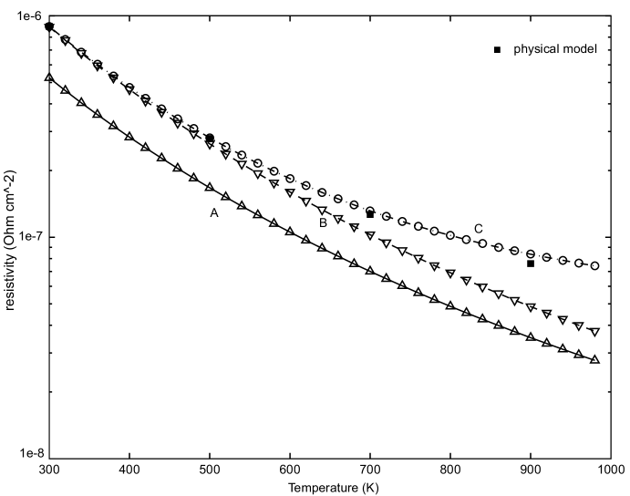
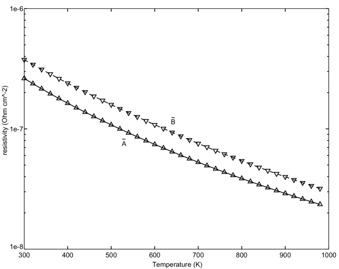
In Fig.2 is the contact resistivity obtained from simulations of the physical model for and , respectively. We firstly compare it with results from a numerical model, namely model A. In model A, the parabolic potential variation is assumed by substituting Eqn. 4 into Eqn. 7, which gives
| (13) |
In this model, quasi-Fermi level is regarded as flat in silicon, i.e. Eqn. 12 is used. It can be seen in Fig. 2 that severe discrepancy of calculated resistivity exists between the numerical model A and the physical model throughout the entire temperature range. In order to investigate its cause, we compare the potential variation computed from these two models in Fig. 3. It is clearly observed that, the assumption of fully depletion becomes invalid at energies near the quasi-Fermi level. Since the tunneling probability exponentially depends on the tunneling distance, this discrepancy in relation leads to significant difference in the tunneling probability, as shown in Fig. 4. By removing the parabolic band-bending assumption in model A, the accuracy of contact calculation can be greatly improved. For this purpose, the one-dimensional Poisson equation needs to be solved for the depletion region. For M-B statistics, the Poisson equation is expressed as
| (14) | |||||
Multiply on both sides of Eqn. 14 and integrate from to , and we obtain
| (15) |
Express it in terms of and we have
| (16) |
according to the definition of in Eqn. 3. Eqn. 16 therefore defines the potential variation from the exact solution to Poisson equation333After assuming constant quasi-Fermi level and ignoring hole concentrations.. Apply Eqn. 3 and 16 to Eqn. 7 and it is obtained that
| (17) |
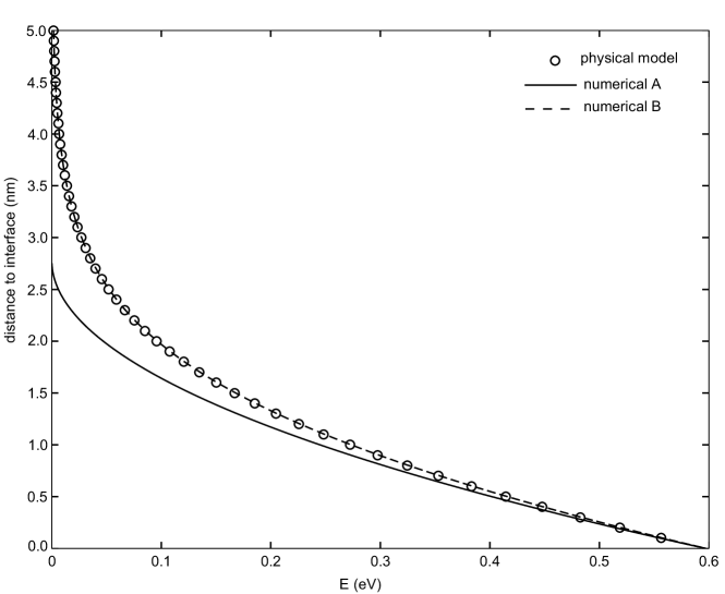
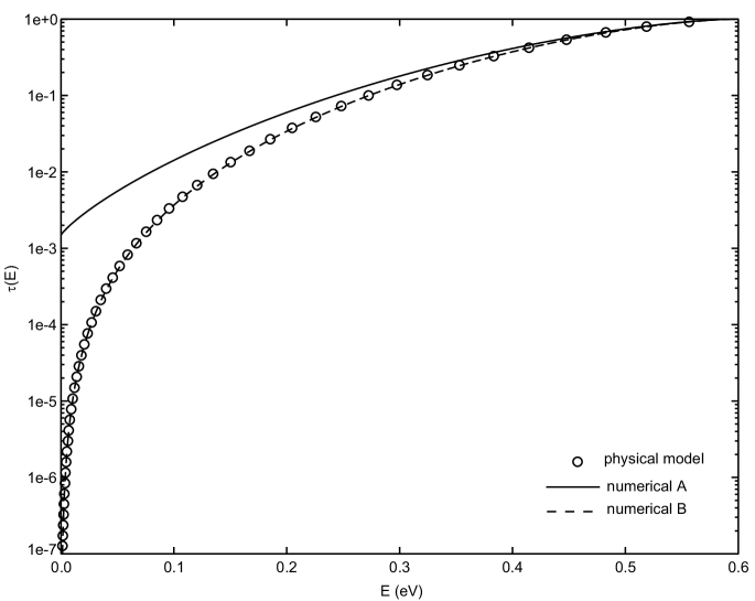
We then have an improved numerical model, namely model B, in which Eqn. 16 and 17 are used to compute the tunneling probability, and constant quasi-Fermi level (Eqn. 12) is still assumed. We also plot the relation and the tunneling probability of model B in Fig.3 and Fig.4, respectively. They show excellent match with those of the physical model. The computed resistivity from model B is also plotted in Fig.2. It can be seen that qualitative improvement is obtained over model A with reference to the physical model. At moderate temperature, the match between model B and the physical model is fairly good. However, an evident discrepancy between them is still observed at high temperature, which is addressed in the next paragraph. As we previously mentioned, our numerical model A, B and the physical model are all based on Eqn. 7, which partially assumed triangular potential barrier a priori. Therefore, it would be interesting to see what the effect of the potential variation is based on the the more general expression of tunneling probability (Eqn. 2). As mentioned earlier, the expression used in [3] (Eqn. 5) is derived from Eqn. 2 by assuming parabolic band-bending completely. We use their expression Eqn. 5 in numerical model . In another numerical model we use the general expression Eqn. 2 and the realistic band-bending formula Eqn. 16. The contact resistivity computed using these two models are plotted in Fig.5, and similar trend is observed: the assumption of the parabolic band-bending severely under-estimates the resistivity at all temperature range.
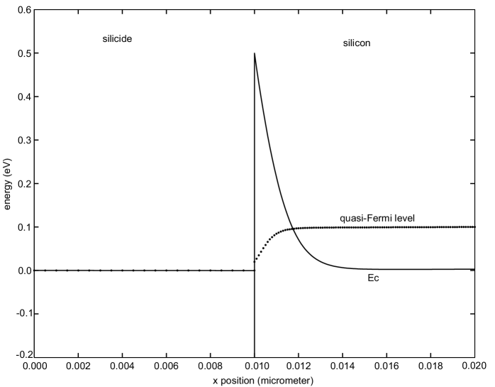
As shown in Fig.2, significant discrepancy in calculated resistivity exists at high temperature between numerical model B and the physical model. However, it can be seen from Fig.4 that the tunneling probability matches for the two models. Therefore, the source of this discrepancy originates from the assumption of constant in the derivation from Eqn. 10 to Eqn. 11. In Fig.6 is the band-diagram of a Schottky contact simulated by the physical model for forward bias . The variation of the electron quasi-Fermi level within the depletion region is evident due to finite carrier supply rate by drift-diffusion. If we let , we expect this variation to approach zero at the same time. But the ratio can be finite in this limit. Since the resistivity is a differential quantity, it can be affected by this effect. However, it should be noted that the validity of drift-diffusion model in the depletion region is an open question itself, since the depletion width is comparable to electron mean free path. If the carrier supply is not limited by the drift-diffusion process, the variation of quasi-Fermi level can be negligible. A possible way to examine this problem is Monte Carlo simulation. The electron continuity equation is
| (18) |
where is electron flux due to carrier transport in the depletion region, and is tunneling flux density. Plug in the tunneling probability and integrate from to and we obtain that
| (19) | |||||
| (20) | |||||
| (21) |
If we assume the electron transport in the depletion region can be modeled as drift-diffusion, as in the physical model, the electron flux can also be expressed as
| (22) | |||||
where is electron mobility. Compare Eqn. 21 and 22 and let , then we obtain
| (23) |
or equivalently,
| (24) |
The inverse of resistivity near zero bias is then revised as
| (25) |
The resistivity calculated using this improved model (model C) is also plotted in Fig.2, and excellent match with the results of the physical model is observed.
References
- [1] M.-C. Jeng, J. E. Chung, P.-K. Ko, and C. Hu, IEEE Trans. Elec. Dev. 37, 2408 (1990).
- [2] F. A. Padovani and R. Stratton, Solid-State Electronics 9, 695 (1966).
- [3] C. R. Crowell and V. L. Rideout, Solid-State Electronics 12, 89 (1969).
- [4] A. Y. C. Yu, Solid-State Electronics 13, 239 (1970).
- [5] K. Matsuzawa, K. Uchida, and A. Nishiyama, IEEE Trans. Elec. Dev. 47, 103 (2000).
- [6] J. Bardeen, Phys. Rev. Lett. 6, 57 (1961).
- [7] W. A. Harrison, Physcal Review 123, 85 (1961).
 |
 |
 |
 |
 |
 |