Simultaneous measurements of electronic conduction and Raman response in molecular junctions
Abstract
Electronic conduction through single molecules is affected by the molecular electronic structure as well as by other information that is extremely difficult to assess, such as bonding geometry and chemical environment. The lack of an independent diagnostic technique has long hampered single-molecule conductance studies. We report simultaneous measurement of the conductance and the Raman spectra of nanoscale junctions used for single-molecule electronic experiments. Blinking and spectral diffusion in the Raman response of both para-mercaptoaniline and a fluorinated oligophenylyne ethynylene correlate in time with changes in the electronic conductance. Finite difference time domain calculations confirm that these correlations do not result from the conductance modifying the Raman enhancement. Therefore, these observations strongly imply that multimodal sensing of individual molecules is possible in these mass-producible nanostructures.
The molecular-scale limits of electronic conduction are of fundamental scientific interest and relevant to future technologies. Our understanding of electronic conduction through single small molecules has grown dramatically in the last decade thanks to improved techniques, including mechanical break junctionsReedetAl97Science ; HeetAl06FD ; VenkataramanetAl06NL single-molecule transistors (SMTs)ParketAl00Nature ; ParketAl02Nature ; LiangetAl02Nature ; KubatkinetAl03Nature ; YuetAl04NL ; PasupathyetAl04Science ; YuetAl04PRL ; PasupathyetAl05NL ; ChampagneetAl05NL ; YuetAl05PRL ; HeerscheetAl06PRL ; ChaeetAl06NL ; DanilovetAl06NL ; vanderZantetAl06PSSB ; NatelsonetAl06CP ; DanilovetAl07NL , nanoparticle dimersDadoshetAl05Nature , noise characterizationDjukicetAl06NL , and thermopower measurementReddyetAl07Science . A major complication in interpreting these experiments is the lack of local imaging or spectroscopic tools that can assess the environment and presence of the molecule of interest.
Over the same period, single-molecule spectroscopies have progressed substantially. In particular, surface-enhanced Raman spectroscopy (SERS) has been demonstrated with single-molecule sensitivityKneippetAl97PRL ; NieetAl97Science ; XuetAl99PRL ; MichaelsetAl00JPCB in random aggregates of metal nanoparticles, though this level of detection is very challenging to prove conclusively. The electromagnetic component of SERS enhancement results from the excitation of surface plasmons in the metal, leading to local fields at the molecule enhanced by a factor of relative to the incident field. The Raman cross section is then enhanced by , where and are the frequencies of the incident and Raman-scattered radiation, respectively. Electromagnetic SERS enhancements exceeding are needed to approach single-molecule detection for many molecules without resonant Raman effectsLeRuetAl07JPCC . Additional “chemical” enhancement is also possible due to electronic interactions between the molecule and the metal. The vibrational modes observed in SERS reflect both the molecule and the local environment and conformation of the molecule on the metal surface. Using a sharp tip to provide a very large local field enhancement, Raman sensitivity has approached the single-molecule levelNeascuetAl06PRB ; DomkeetAl06JACS . Very recently we found that nanoscale gaps between extended electrodes are very effective as extremely confined SERS hotspots and may be mass produced with relatively high yields.WardetAl07NL
In this paper we use these nanoscale gap structures to perform simultaneous measurements of electronic transport and SERS. In many previous papersParketAl00Nature ; ParketAl02Nature ; LiangetAl02Nature ; KubatkinetAl03Nature ; YuetAl04NL ; PasupathyetAl04Science ; YuetAl04PRL ; PasupathyetAl05NL ; ChampagneetAl05NL ; YuetAl05PRL ; HeerscheetAl06PRL ; ChaeetAl06NL ; DanilovetAl06NL ; vanderZantetAl06PSSB ; NatelsonetAl06CP ; DanilovetAl07NL it has been established that conductance in such structures is dominated by roughly a molecular volume. The conductance as a function of time is observed to correlate strongly with the SERS signal in 11% of the junctions measured. Conductance changes correlate with sudden changes in the intensity of sets of Raman modes (“blinking”) and with spectral diffusion of mode positions. The data suggest that both SERS and conductance changes are most likely due to changes in conformation and binding of an individual molecule. The combined data provide a great deal of information about the effect of molecular orientation and environment on both conduction and SERS, although a detailed understanding of this correlated information is indeed a very significant theoretical challenge. The most likely explanation for these results is that single-molecule multimodal sensing is possible. This combined measurement technique also opens the possibility of direct assessment of vibrational pumping and local heating in single-molecule electronic transport.
Our nanogap structures are fabricated on 1 cm2 pieces of -doped Si wafer with 200 nm of thermal silicon oxide. The structures are defined using electron-beam lithography and e-beam evaporation of 1 nm Ti and 15 nm of Au. The initial nanoconstriction structure consists of two large pads connected by a single constriction as shown in Figure 1. The constriction is approximately 500 nm long and 100-180 nm wide. Liftoff is performed in acetone or chloroform and the samples are then cleaned of organic residue by 1 minute exposure to O2 plasma. For devices incorporating para-mercaptoaniline (pMA), samples are immediately placed in a 1 mM solution of pMA in ethanol. Samples are soaked in the pMA solution for 12 to 24 hours as pMA self-assembles on the Au surfaces, followed by an ethanol rinse to remove any excess pMA. We have also measured devices using a fluorinated oligophenylene ethynylene (FOPE)HamadanietAl06NL that possesses a distinctive Raman spectrum (see Supporting Information). FOPE was assembled via standard base deprotectionTouretAl95JACS from a 0.25 mg/mL solution of the thioacetate form of the molecules in 1:1 ethanol-chloroform solvent, prepared under dry N2 gas.
The nanoconstrictions are converted into nanogaps via electromigrationParketAl99APL , a thoroughly studiedStrachanetAl06NL ; TaychatanapatetAl07NL process dominated by momentum transfer from current-carrying electrons to mobile atoms in the metallic lattice. Electromigration has been used extensively to prepare electrodes for single-molecule conduction measurements, with typical yields of 10-20% for tunneling gaps inferred to contain individual molecules (based on statistics on thousands of junctions)ParketAl00Nature ; ParketAl02Nature ; LiangetAl02Nature ; YuetAl04NL ; PasupathyetAl04Science ; YuetAl04PRL ; PasupathyetAl05NL ; ChampagneetAl05NL ; YuetAl05PRL ; HeerscheetAl06PRL ; ChaeetAl06NL ; vanderZantetAl06PSSB ; NatelsonetAl06CP . Each gap is electromigrated with an automated procedure to form an atomic-scale constriction with a resistance of 3 k, which is then allowed to break spontaneouslyO'NeilletAl07APL . While the atomic-scale details of each gap are different, gaps with measurable tunneling currents are formed routinely with high yield, and recent advances in it situ electron microscopyStrachanetAl06NL ; HeerscheetAl07APL do, in principle, permit detailed structural examinations of the resulting electrodes. The migration and subsequent electrical measurements are performed in situ on the sample stage of the Raman measurement system, in air at room temperature.
Electrical contact to the junction under test is made via micropositionable probes. One digital lock-in amplifier (SRS SR830) is used to source 50-100 mV RMS at 200 Hz onto one pad, while the other pad is connected to a current-to-voltage converter (either SRS SR570 or Keithley 482). The AC current () and its second harmonic () are measured with lock-in amplifiers, while the DC component of the current is sampled at 5.0 kHz. The unusually large AC bias (much larger than necessary to measure differential conductance alone) is required because of an unanticipated complication: the illuminated, molecule-decorated nanogaps can also exhibit significant DC photocurrents due to optical rectification (to be described in a separate publication). The large AC bias is needed so that the AC current is detectable without the DC current signal overloading the lock-in input stages. We find no evidence that the 100 mV RMS AC bias degrades the nanogap or the assembled molecules.
Optical measurements are performed using a WITec CRM 200 scanning confocal Raman microscope in reflection mode. Devices are illuminated by a 785 nm diode laser at normal incidence with a diffraction-limited spot. A 100x ultra-long working distance objective leaves sufficient room for the micromanipulated electrical probes to be inserted between the objective and sample.
As reported previously, the electromigrated nanogaps are outstanding substrates for SERS.WardetAl07NL Initially, spatial maps of the underlying Si of unmigrated nanogaps are obtained to facilitate centering of the Raman microscope over the nanogap to within 100 nm. Spatial maps of the integrated molecular Raman signal after electromigration demonstrate the localization of the SERS hotspot (Fig. 1D, E). Raman spectra are taken with 1 s or 2 s integration times while the microscope objective is held fixed over the migrated junctions. Electrical measurements on unbroken constrictions under various illumination conditions demonstrate that heating of the electrodes due to the laser is not significant. The inferred change in the electrode temperature at 0.5 mW laser power was less than 2 K (see Supporting Information).
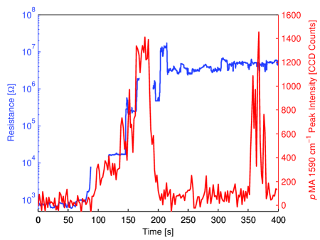
When the conductance of the junction drops below the conductance quantum, , a tunneling gap is formed, and simultaneous conductance and Raman measurements are performed. In situ measurements of the optical response of nanogaps during migration are presented in Figure 2. Even prior to complete nanogap formation, partially electromigrated junctions show SERS enhancement of the assembled molecules once the resistance exceeds about 1 k. The appearance of SERS indicates that the local interelectrode plasmon modes are now excitable. Crudely, this implies that over an optical cycle the junction acts more like a capacitor than a resistor; that is, the time constant of the nanogap is comparable to one optical period. For a 1 k nanogap illuminated at 785 nm this implies an effective nanogap capacitance at optical frequencies on the order of 10s of attofarads.
The measured Raman signal strength scales logarithmically with the resistance of the gap until resistances exceed 1-10 M. At higher gap resistances, the Raman signal takes on a roughly constant value with sporadic changes (corresponding to SERS blinking events). This decoupling of electronic transport and SERS at low conductances is not surprising a priori, since tunneling conductances vary exponentially with gap size, while local plasmonic structure is less sensitive. Blinking events are often not correlated with further changes in junction resistance. This means that molecules are present in a region of strong Raman enhancement, while the molecular-scale tunneling volume dominating interelectrode conductance does not contain molecules that are detectably contributing to the Raman signal. We discuss this further below.
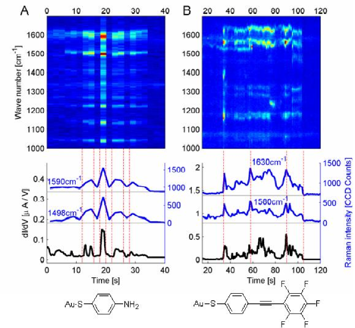
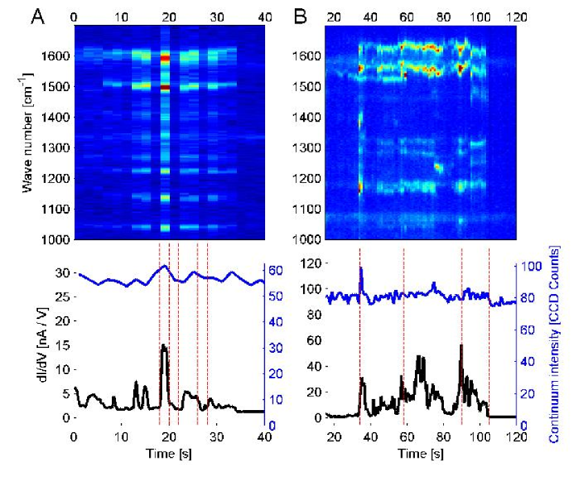
However, in 17 of 120 junctions using pMA and 4 out of 70 junctions using FOPE, there are strong temporal correlations between the fluctuations in the nanogap conductance and changes in the SERS spectrum. This yield is quantitatively consistent with the yield of tunneling gaps containing single molecules inferred in single-molecule transistor measurements. Examples are shown in Figures 3 and 4 (with further examples in the Supporting Information). In Figure 3A a simple positive correlation between Raman intensity and is observed for all Raman modes. In Figure 3B another positive correlation between Raman intensity and differential conductance is observed in a different junction. In this case spectral diffusion of the Raman lines occurs but does not correlate significantly with the conduction. In both Figs. 3A and 3B the amplitudes (count rates) of strong Raman modes have similar relative changes as the differential conductance.
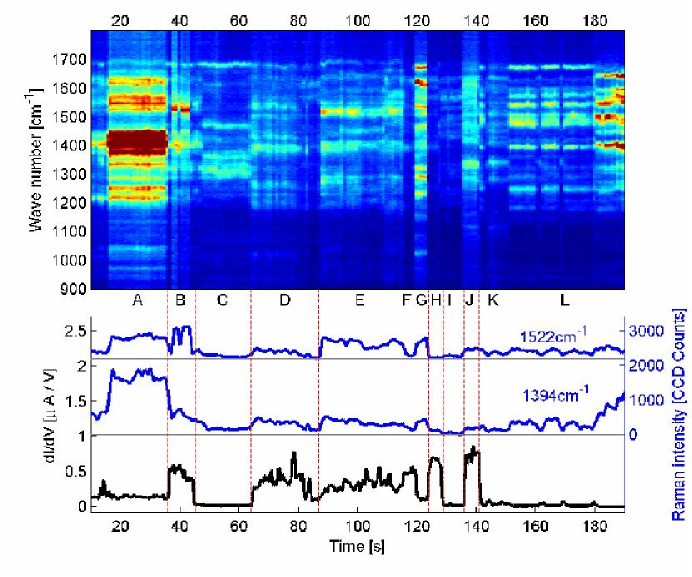
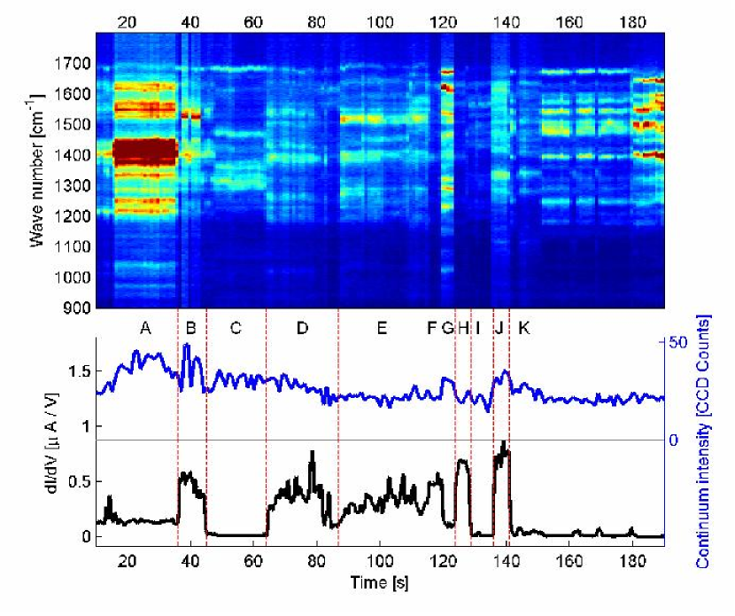
Figure 4 is an example of a more complicated relationship between the conductance and the SERS spectrum. While sudden changes in the Raman spectrum are correlated in time with changes in the measured conductance, some increases in Raman intensity correlate with increased conductance, while others correlate with decreases in conductance. Additionally, changes in the mode structure of the Raman spectrum clearly correlate with changes in conductance. In region A the Raman spectrum and conductance are constant; when the Raman spectrum changes in region B a three-fold increase in conductance is observed, though overall Raman intensity changes only for certain modes. In region C the spectrum changes yet again, and while a weaker Raman spectrum remains, the conduction drops significantly. In region D the same mode structure seen in B returns and the conduction is similar to that seen in B as well. Regions D and E have positive correlations between Raman intensity and conduction with the lowest conduction observed between D and E where the Raman intensity is also lowest. At F a switch from positive to negative correlation between the Raman intensity and conduction occurs and carries over to regions G and H. At region I a small change in the mode structure is observed correlating with a switch to positive intensity-conduction correlations, continuing through regions J and K. In region L there is a final change in mode structure resulting in negative intensity-conduction correlations exemplified in the three conduction spikes that occur when the Raman spectrum disappears.
It should be noted that our pMA spectra are typically dominated by the symmetry modesOsawa94JPhysChem , as was seen previouslyWardetAl07NL . This is not surprising, as it is well accepted that symmetry modes experience additional ”chemical” enhancements in comparison to symmetry modes. We often only observe the 1590 cm-1 symmetry peak and not the other expected mode at 1077 cm-1. Strong spectral diffusion in both molecules with shifts as large as 20 cm-1 have also been observed, and are clear in Fig. 3b. This surely limits direct comparison to spectra reported elsewhere. However, the measured spectra are quite consistent with one another and are qualitatively different than those seen in “bare” junctions contaminated by physisorbed exogenous carbonWardetAl07NL .
One possible concern could be that changes in metal configuration at the junction are responsible for the fluctuations in tunneling conductance and SERS intensity. This scenario is unlikely for several reasons. First, tunneling conductances depend exponentially on gap geometry; while could change by a factor of ten for a 0.1 nm change in gap separation, it is very unlikely that the electromagnetic enhancement would be as strongly affected. Second, it is not clear how metal rearrangement could explain the observed changes in Fig. 4; this would require that the gap itself alternately grow and shrink, with some changes in metal geometry giving large features with small Raman effects and others vice versa. Finally, during the events in Figs. 3 and 4, the continuum emission at low wavenumbers observed previously due to inelastic light scattering from the metal electrodesWardetAl07NL is constant in time (see Supporting Information).
Another concern is that changes in tunneling conduction in one part of the junction may alter the plasmon mode structure and affect Raman emission from elsewhere in the junction. Such a scenario could lead to correlations like those in Figs. 3 and 4 even if conduction and Raman emission are not from the same molecule. Given that the interelectrode conductance affects Raman emission (Fig. 2), it is important to consider this possibility. We have performed finite-difference time domain (FDTD) simulations of the optical properties of such junctions to assess this issue, and the results (vide infra) effectively rule out this concern. While the finite grid size (1 nm) required for practical computation times restricts the quantitative accuracy of these calculations, the main results regarding spatial mode structure and wavelength dependence are robust, and the calculated electric field enhancements are an underestimateOubreNordlander05JPCB ; WardetAl07NL .
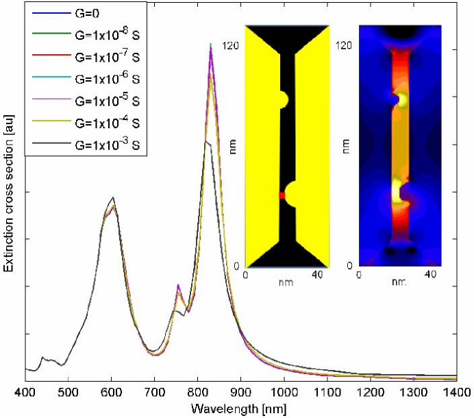
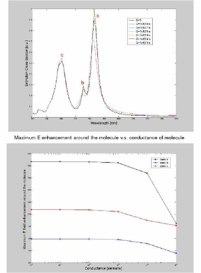
Figure 5 shows a comparison of calculated extinction spectra that characterize the plasmonic mode structure of the gap structure shown, for various values of interelectrode conductance connecting the source and drain at the indicated point. An analysis of the instantaneous charge distribution associated with the plasmon resonances in Fig. 5 shows that negligible charge transfer occurs between the two electrodes for conductances smaller than . The FDTD simulations show that the mode structure and enhancement are unaffected by conductances smaller than a few . Details are presented in Supporting Information. These calculations confirm the interpretation given above for Fig. 2: The plasmonic mode structure responsible for enhanced local fields in the nanogap is established once the interelectrode conductance falls well below . Given these FDTD results, the only plausible explanation for such strong correlations in time between conduction and Raman emission is that both processes involve the same molecule or molecules.
Conduction in nanogaps is known to be dominated by a tiny volume inferred in single molecule transport and break junction experiments to contain often only one molecule. Molecular movement, changes in bonding, or reorientation of the molecule in the gap results in different tunneling configurations and hence in conductance changes. The complex relationship between conductance and Raman mode structure and intensity is also then natural, since chemical enhancement effects and the appearance of broken symmetry modes should be strongly affected by changes in molecular configuration on the metal surface. It should also be noted that the measured junction conductances are consistent with the expected single molecular conductance range of to G0 measured in similar molecules by break junction techniquesVenkataramanetAl06NL .
The detailed SERS mode structure combined with the conductance contains a wealth of information about the bonding, orientation, and local environment of the molecule. With appropriate electronic structure calculations and theoretical estimates of the Raman tensor for candidate molecule/metal configurations, it should be possible to infer likely junction geometries and chemical structure corresponding to each type of Raman spectrum. Such calculations are very challenging even for the conductance distribution aloneQueketAl07arxiv .
These conductance/Raman observations and accompanying calculations demonstrate that electromigrated nanogaps between extended electrodes can achieve enhancements sufficient for single-molecule SERS sensitivity. Given that these structures can be fabricated in a scaleable manner in predefined locations with high yieldsWardetAl07NL , this may allow significant advances in SERS-based sensing as well as multimodal sensing. With further improvements in technique (e.g., measurements in vacuum as a function of temperature, interelectrode bias, and gate voltage in a SMT configuration), it will be possible to address open fundamental issues in SERS, including the nature of chemical enhancement, the mechanism of blinking, and the cause of the large spectral diffusion of Raman lines. Finally, comparisons of Stokes and anti-Stokes Raman peak intensities as a function of bias across the junction can reveal whether current flow pumps particular vibrational modes out of thermal equilibrium. This would enable new and detailed studies of nonequilibrium physics and chemistry at the single molecule scale. Comparisons between these results and transport/Raman studies on molecular ensemblesNowaketAl04JACS ; JaiswaletAl06AC should also provide valuable information about the effect of molecular environment on these processes.
DW acknowledges support from the NSF-funded Integrative Graduate Research and Educational Training (IGERT) program in Nanophotonics. NH, DN, and PN acknowledge support from Robert A. Welch Foundation grants C-1220, C-1636, and C-1222, respectively. DN also acknowledges NSF award DMR-0347253, the David and Lucille Packard Foundation, the Sloan Foundation, and the Research Corporation. JMT acknowledges support from DARPA and AFOSR.
Supporting Information Available: Detailed examination of laser heating, continuum background, extended discussions of FDTD calculations, and more example data sets. This material is available free of charge via the Internet at http://pubs.acs.org.

References
- (1) Reed, M. A.; Zhou, C.; Muller, C. J.; Burgin, T. P.; Tour, J. M. Science 1997, 278, 252-254.
- (2) He, J.; Sankey, O.; Lee, M.; Tao, N. J.; Li, X.; Lindsay, S. Faraday Discuss. 2006, 131, 145-154.
- (3) Venkataraman, L.; Klare, J. E.; Tam, I. W.; Nuckolls, C.; Hybertsen, M. S.; Steigerwald, M. L. Nano Lett. 2006, 6, 458-462.
- (4) Park, H.; Park, J.; Lim, A. K. L.; Anderson, E. H.; Alivisatos, A. P.; McEuen, P. L. Nature 2000, 407, 57-60.
- (5) Park, J.; Pasupathy, A. N.; Goldsmith, J. I.; Chang, C.; Yaish, Y.; Petta, J. R.; Rinkowski, M.; Sethna, J. P.; Abruña, H. D.; McEuen, P. L.; Ralph, D. C. Nature 2002, 417, 722-725.
- (6) Liang, W.; Shores, M. P.; Bockrath, M.; Long, J. R.; Park, H. Nature 2002, 417, 725-729.
- (7) Kubatkin, S.; Danilov, A.; Hjort, M.; Cornil, J.; Brèdas, J.-L.; Stuhr-Hansen, N.; Hedeg rd, P.; Bjørnholm, T. Nature 2003, 425, 698-701.
- (8) Yu, L. H.; Natelson, D. Nano Letters 2004, 4, 79-83.
- (9) Pasupathy, A. N.; Bialczak, R. C.; Martinek, J.; Grose, J. E.; Donev, L. A. K.; McEuen, P. L.; Ralph, D. C. Science 2004, 306, 86-89.
- (10) Yu, L. H.; K., K. Z.; Ciszek, J. W.; L., C.; Stewart, M. P.; Tour, J. M.; Natelson, D. Phys. Rev. Lett. 2004, 82, 266802.
- (11) Pasupathy, A. N.; Park, J.; Chang, C.; Soldatov, A. V.; Lebedkin, S.; Bialczak, R. C.; Grose, J. E.; Donev, L. A. K.; Sethna, J. P.; Ralph, D. C.; McEuen, P. L. Nano Lett. 2005, 5, 203-207.
- (12) Champagne, A. R.; Pasupathy, A. N.; Ralph, D. C. Nano Lett. 2005, 5, 305-308.
- (13) Yu, L. H.; Keane, Z. K.; Ciszek, J. W.; Cheng, L.; Tour, J. M.; Baruah, T.; Pederson, M. R.; Natelson, D. Phys. Rev. Lett. 2005, 95, 256803.
- (14) Heersche, H. B.; Groot, de Z.; Folk, J. A.; Zant, van der H. S. J.; Romeike, C.; Wegewijs, M. R.; Zobbi, L.; Barreca, D.; Tondello, E.; Cornia, A. Phys. Rev. Lett. 2006, 96, 206801.
- (15) Chae, D.-H.; Berry, J. F.; Jung, S.; Cotton, F. A.; Murillo, C. A., Yao, Z. Nano Lett. 2006, 6, 165-168.
- (16) Danilov, A. V.; Kubatkin, S. E.; Kafanov, S. G.; Flensberg, K.; Bjørnholm, T. Nano Lett. 2006, 6, 2184-2190.
- (17) Zant, van der H. S. J.; Osorio, E. A.; Poot, M.; O’Neill, K. phys. stat. sol (b) 2006, 243, 3408-3412.
- (18) Natelson, D.; Yu, L. H.; Ciszek, J. W.; Keane, Z. K.; Tour, J. M. Chem. Phys. 2006, 324, 267-275.
- (19) Danilov, A. V.; Kubatkin, S. E.; Kafanov, S. G.; Hedegård, P.; Stuhr-Hansen, N.; Moth-Poulsen, K.; Bjornholm, T. Nano Lett. 2007, in press.
- (20) Dadosh, T.; Gordin, Y.; Krahne, R.; Khivrich, I.; Mahalu, D.; Frydman, V.; Sperling, J.; Yacoby, A.; Bar-Joseph, I. Nature 2005, 436, 677-680.
- (21) Djukic, D.; Ruitenbeek, van J. M. Nano Lett. 2006, 6, 789-793.
- (22) Reddy, P.; Jang, S.-Y.; Segalman, R. A.; Majumdar, A. Science 2007, 315, 1568-1571.
- (23) Kneipp, K.; Wang, Y.; Kneipp, H.; Perelman, L. T.; Itzkan, I.; Dasari, R.; Feld, M. S. Phys. Rev. Lett. 1997, 78, 1667-1670.
- (24) Nie, S.; Emory, S. R. Science 1997, 275, 1102-1106.
- (25) Xu, H.; Bjerneld, E. J.; Käll, M.; Börjesson, L. Phys. Rev. Lett. 1999, 83, 4357-4360.
- (26) Michaels, A. M.; Jiang, J.; Brus, L. J. Phys. Chem. B 2000, 104, 11965-11971.
- (27) Le Ru, E. C.; Blackie, E.; Meyer, M.; Etchegoin, P. G. J. Phys. Chem. C 2007, 111, 13794-13803.
- (28) Neascu, C. C.; Dreyer, J.; Behr, N.; Raschke, M. B. Phys. Rev. B 2006, 73, 193406.
- (29) Domke, K. F.; Zhang, D.; Pettinger, B. J. Am. Chem. Soc. 2006, 128, 14721-14727.
- (30) Ward, D. R.; Grady, N. K.; Levin, C. S.; Halas, N. J.; Wu, Y.; Nordlander, P.; Natelson, D. Nano Lett. 2007, 7, 1396-1400.
- (31) Hamadani, B. H.; Corley, D. A.; Ciszek, J. W.; Tour, J. M.; Natelson, D. Nano Lett. 2006, 6, 1303-1306.
- (32) Tour, J. M.; Jones, L., II; Pearson, D. L.; Lamba, J. S.; Burgin, T. P.; Whitesides, G. W.; Allara, D. L.; Parikh, A. N.; Atre, S. J. Am. Chem. Soc. 1995, 117, 9529-9534.
- (33) Park, H.; Lim, A. K. L.; Alivisatos, A. P.; Park, J.; McEuen, P. L. Appl. Phys. Lett. 1999, 75, 301-303.
- (34) Strachan, D. R.; Smith, D. E.; Fischbein, M. D.; Johnston, D. E.; Guiton, B. S.; Drndi’c, M.; Bonnell, D. A.; Johnson Jr., A. T. Nano Lett. 2006, 6, 441-444.
- (35) Taychatanapat, T.; Bolotin, K.; Kuemmeth, F.; Ralph, D. C. Nano Lett. 2007, 7, 652-656.
- (36) O’Neill, K.; Osorio, E. A.; van der Zant, H. S. J. Appl. Phys. Lett. 2007, 90, 133109.
- (37) Heersche, H. B.; Lientschnig, G.; O’Neill, K.; van der Zant, H. S. J.; Zandbergen, H.W. Appl. Phys. Lett. 2007, 91, 072107.
- (38) Osawa, M.; Matsuda, N.; Yoshii, K.; Uchida, I. J. Phys. Chem. 1994, 98, 12702-12707.
- (39) Oubre, C.; Nordlander, P. J. Phys. Chem. B 2005, 109, 10042-10051.
- (40) Quek, S. Y.; Venkataraman, L.; Choi, H. J.; Louie, S. G.; Hybertsen, M. S.; Neaton, J. B. Nano Lett. 2007, 7, 3477-3482.
- (41) Nowak, A. M.; McCreery, R. L. J. Am. Chem. Soc. 2004, 126, 16621-16631.
- (42) Jaiswal, A.; Tavakoli, K. G.; Zou, S. Anal. Chem. 2006, 78, 120-124.
Supporting Information:
Simultaneous measurements of electronic conduction and Raman response in molecular junctions
I Laser Heating
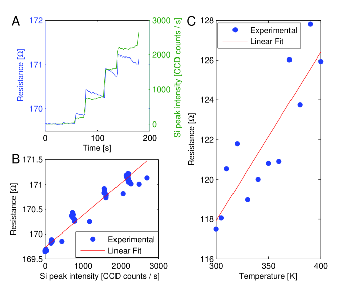
To determine the effects of laser heating on nanogaps, unbroken constrictions were illuminated with various laser powers while the resistance was measured as seen in Figure S1A. To determine the laser power we measured the number of CCD counts per second in the Si 520 cm-1 peak. At higher laser powers irreversible changes to the constriction occur as evident in the dropping resistance of the constriction when the laser power is held constant. We do not believe that such changes in the constriction will dramatically change our estimate of the laser heating. These laser powers are much higher than used in our conduction experiment where we expect about 50 CCD counts per second in the Si peak. From our measurements we determined the resistance of the constriction as a function of laser power as shown in Figure S1B using a linear least-squares fit. The final resistance/laser intensity relationship of , where is the resistance in Ohms and the laser intensity in Si CCD counts/second, is based on the average of three different samples.
We then took different devices from the same sample chip and heated them in a probe station while measuring their resistance, as seen in Figure S1C. A linear fit was performed to determine the resistance as a function of temperature this time averaging over four samples. The final relationship was determined to be , where is the resistance in Ohms and is the temperature in Kelvin. Equating our two relationships we find that the change in temperature per CCD count in the Si peak is 0.012 K. At the laser power used in our conduction experiments (50 CCD counts/second) this lets us estimate a temperature change of 0.62 K due to illumination.
II Additional examples
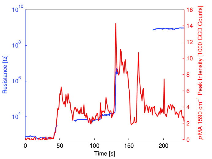
Figure S2 is a second example of the evolution of SERS response during the electromigration process. As in Fig. 1 of the main manuscript, Raman response becomes detectable at the nanojunction once the electromigrated two-terminal resistance exceeds 1-2 k. This implies that the localized interelectrode plasmon modes responsible for the enhanced local electric field are established before the junction is entirely broken. As discussed in the main text, a simple interpretation of this is that once the charge relaxation time across the nanoconstriction significantly exceeds the duration of an optical cycle, the coupling between the two sides of the junction is chiefly capacitive rather than conductive.
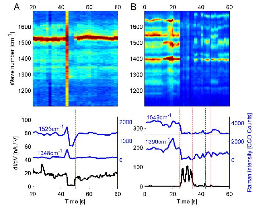
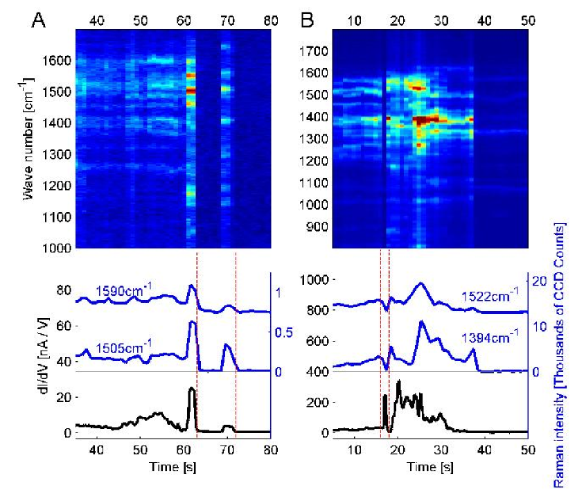
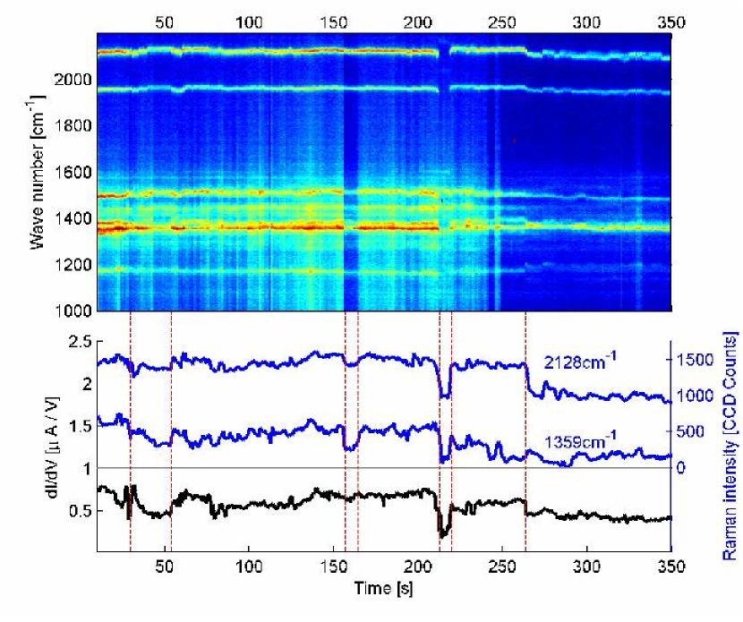
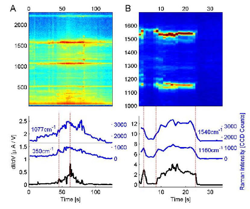
Figures S3-S5 are additional examples of pMA Raman spectra that correlate in time with measured junction conductance. Figure S6 shows similar data from one FOPE device and another pMA device. Sometimes the relationship between SERS intensity and is simple, as in Fig. S3A and S4A: increased Raman intensity correlates with increased conductance. However, in some devices decreases in SERS intensity, particularly of modes, correlates with increased conductance, as in Figs. S3B and S4B. More complicated situations can also arise, as in Fig. S5, where conductance changes appear to correlate with both changes in Raman intensity and with the onset of spectral diffusion of some modes. These data contain much information implicit about the orientation of the molecule, its bonding to the metal atoms of the electrodes, and the local chemical environment. A realistic theoretical treatment that encompasses these necessary ingredients is beyond the scope of this paper.
III Continuum emission at low wavenumbers
As mentioned in the text, in these electromigrated junctions there is enhanced continuum Raman emission at low wavenumbers. This emission results from inelastic light scattering via the conduction electrons in the metal, and is present in junctions without molecules. Note that in devices with molecules, in extremely strong SERS blinks (brief periods of strong Raman emission), some increase in emission at low wavenumbers does occur, though this is much more modest than the percentage changes seen molecule-specific Raman modes. Figures S7 and S8 are reproductions of the Raman data from Figures 3 and 4 of the main manuscript, but with the conductance as a function of time plotted in comparison to the integrated continuum emission (70 cm-1 - 100 cm-1). During the major conductance changes and Raman blinking events, the continuum emission changes much less than either the SERS intensity or the conductance. This strongly suggests that the metal configuration at the junction is not changing in time; rather, the changes in SERS intensity and conductance are therefore due to changes in the molecular position, orientation, and chemical environment.
IV FOPE molecule
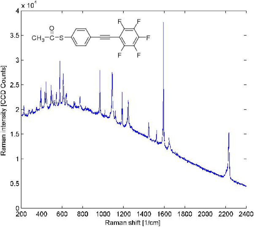
Figure S9 shows the Raman spectrum for a bulk crystal of the FOPE molecule, first reported by Hamadani et al.[S1] The mode at approximately 2210 cm-1 is the symmetric stretch of the carbon-carbon triple bond. The full name of FOPE is thioacetic acid 4-pentafluorophenylethynyl-phenyl ester, and its synthesis and characterization are reported in the supplemental material to the above paper.
V FDTD calculations
The optical properties of the bowtie structure were calculated using the Finite-Difference Time-Domain method (FDTD) using a Drude dielectric function with parameters fitted to the experimental data for gold. This fit provides an accurate description of the optical properties of gold for wavelengths larger than 500 nm.[S2] These calculations do not account for reduced carrier mean free path due to surface scattering in the metal film, but such an effect is unlikely to change the results significantly.
The bowtie is modeled as a two finite triangular structures as partially illustrated in Fig. 5, left inset, of the manuscript. Our computational method requires the nanostructures to be modeled to be of finite extent. The plasmon modes of a finite system are standing modes with frequencies determined by the size of the sample and the number of nodes of the surface charge distribution associated with the plasmon. For an extended system such as the bowties manufactured in this study, the plasmon resonances can be characterized as traveling surface waves with a continuous distribution of wavevectors.
Previous calculations of a series of calculations of bowties with increasing length reveals that the optical spectrum is characterized by increasingly densely spaced plasmon resonances in the wavelength regime 500-1000 nm and a low energy finite-size induced split-off state involving plasmons localized on the outer surfaces of the bowtie. For a large bowtie, we expect the plasmon resonances in the 500-1000 nm wavelength interval to form a continuous band.[S3,S4]
To investigate the effects of a conductance shunting the nanoscale gap, FDTD calculations were performed for a bowtie with two semi-spherical protrusions in the junction as shown in the close-up in the inset of Fig. 5 of the main text. The electrodes are modeled as regular trapezoids of a height of 50 nm, and a 1 nm grid size was used. The conductance was modeled as a cubical volume 2 nm on a side located between the 6 nm radius asperity and the facing electrode, where the local field enhancement is maximized for modes relevant to the wavelengths used in the experiment. The conductivity of the material was set to be frequency independent over the wavelength range of interest (as expected for tunneling), and chosen such that the conductance of that interelectrode link was the desired value.
Figure S10(top) reproduces the main portion of Fig. 5 from the main text. The three most prominent features in the calculated extinction spectrum are labeled. Peak “a” corresponds to the mode shown in Fig. 5 of the main text, believed to be most relevant for the experiments at hand. Figure S10(bottom) shows the evolution of the electric field enhancement factor (calculated for the mid-point of the conducting volume standing in for the molecule) as a function of interelectrode conductance. The field enhancement and mode shapes due to local features in the junction are essentially unaffected by the interelectrode conductance until that conductance exceeds the order of S. For conductances significantly larger than , charges can flow between the two electrodes and a new low energy plasmon resonance appears at wavelengths that depend on the conductance of the shunt. This is completely consistent with the observations in Fig. 2 of the main paper and Fig. S1 of this supporting material. This demonstrates that the conductance changes in these experiments are not able to modify Raman emission from other molecules not in the tunneling region.
[S1] Hamadani, B. H.; Corley, D. A.; Ciszek, J. W.; Tour, J. M.; Natelson, D. Nano Lett. 2006, 6, 1303-1306.
[S2] Oubre, C.; Nordlander, P. J. Phys. Chem. B 108, 108, 17740-17747.
[S3] Nordlander, P.; Le, F. Appl. Phys. B 2006, 84, 35-41.
[S4] Ward, D. R.; Grady, N. K.; Levin, C. S.; Halas, N. J.; Wu, Y.; Nordlander, P.; Natelson, D. Nano Lett. 2007, 7, 1396-1400.