Magnetically induced spin-dependent photoemission from -GaAs(Cs,O) into vacuum
Abstract
A spin-dependent emission of optically oriented electrons from -GaAs(Cs,O) into vacuum was experimentally observed in a magnetic field normal to the surface. This phenomenon is explained within the model which takes into account the jump in the electron factor at the semiconductor-vacuum interface. Due to this jump, the effective electron affinity on the semiconductor surface depends on the mutual direction of optically oriented electron spins and the magnetic field, resulting in the spin-dependent photoemission. It is demonstrated that the observed effect can be used for the determination of spin diffusion length in semiconductors.
pacs:
72.25.Fe, 72.25.Mk, 78.20.Ls, 79.60.DpI Introduction
Investigations of spin-polarized electron transport through various interfaces in solid-state structures constitute an important domain of spintronics and have been an area of active research for over ten years.Awschalom1 In this context, studies of the emission process of optically oriented electrons from semiconductors with the state of effective negative electron affinityBell2 (NEA) are of both applied and fundamental interest. The application prospects are related to the development of spin detectors for low energy electron beamsCacho3 ; Alper4 and of efficient spin-polarized electron sources.Pierce5 ; Prepost6 The scientific interest lies in the elucidation of mechanisms of spin relaxation during transport through a semiconductor-vacuum interface. It is also important that this interface can be considered as a model one at which the energy, effective mass and factor undergo jumps at ultimately small distances of about an interatomic separation. In contrast to the solid-state heterojunctions, in vacuum it is possible to measure not only a total electric current through the interface but also the energy and momentum distributions of emitted electronsDrouhin7 ; Terek8 ; Orlov9 and their spin.Drouhin10 These investigations enable one to clarify the conditions and restrictions for the use of effective electron parameters, such as the effective mass and the effective factor, for the description of charge and spin transfer through abrupt interfaces. Measurements of photoemission with angular and spin resolution open the possibility of studying spin-dependent tunneling of electrons that was predicted in Refs. Voskoboynikov11, ; Perel12, ; Tarasenko13, .
Spin-dependent electron transport, which is caused by the jump in the electron factor at internal semiconductor interfaces, was previously studied in Refs. Gruber14, and Fabian15, . Gruber et al.Gruber14 investigated spin-dependent resonant electron tunneling through the Zeeman levels of a double-barrier structure with a quantum well made of a semimagnetic semiconductor. Fabian et al.Fabian15 theoretically analyzed the dependence of the characteristics of a magnetic junction on the direction of the electron spin with respect to the magnetic field. The phenomena related to the jump of the electron factor at a semiconductor-vacuum interface have not yet been investigated. In this paper we study the transport of spin-polarized electrons through the -GaAs(Cs,O)-vacuum interface. The probability of electrons escaping into vacuum was found to depend on the direction of the electron spin with respect to the magnetic field applied perpendicularly to the surface. The experimental results are described well in the emission model which takes into account the jump in the electron factor at the semiconductor-vacuum interface. The observation of the effect was preliminarily reported in Ref. Orlov16, . In this paper we present data and analysis which yield a self-consistent picture of the spin-dependent photoemission at a semiconductor-vacuum interface. The opportunity to explore this effect for studying spin transport in semiconductors is demonstrated. In particular, the spectrum of the observed effect allowed us to determine the spin diffusion length of electrons in -GaAs.
II Spin-dependent photoemission: a qualitative explanation
A phenomenological expression for the spin-dependent component of photocurrent in a magnetic field H can be written in the following form:
| (1) |
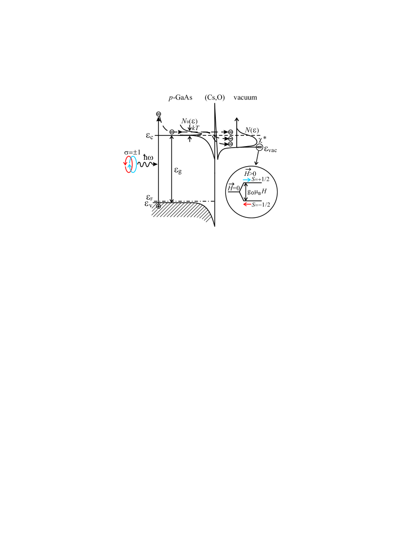
where S is the mean spin of optically oriented electrons and the constant depends on the microscopic mechanism of the effect and determines its relative magnitude. Several microscopic mechanisms of magnetically induced spin-dependent photoemission (SDP) are possible with both bulk and surface origin. Preliminary estimations show that for the case of spin-polarized electrons emitted from -GaAs activated by cesium and oxygen to the state of NEA, a mechanism based on the jump in the factor at the semiconductor-vacuum interface can significantly contribute to SDP. The jump in the factor causes the difference between the NEA values for electrons with spins oriented along or opposite to the magnetic field. This difference results in the dependence of the photoemission current on the direction of electron spin with respect to the magnetic field. This mechanism is illustrated on the energy band diagram of the semiconductor-vacuum interface (Fig. 1) and can be explained as follows. The electrons, which are excited in the conduction band by light with photon energies exceeding the band gap , are thermalized to the band bottom, form a narrow energy distribution with the width of , diffuse towards the emitting surface, pass through the band bending region, and escape into vacuum. Because of the momentum and energy scattering during electron transport across the band bending region and through the (Cs,O) activation layerDrouhin7 ; Terek8 ; Orlov9 , in vacuum the kinetic energy distribution of electrons is broadened up to the magnitude of NEA, , which is defined as the energy difference between the vacuum level and the bottom of the conduction band in the bulk. The electrons, which descend along the energy scale below the vacuum level during thermalization in the band bending region, recombine at the surface and do not contribute to the photoemission current. Therefore, the photoemission quantum yield, as well as the photocurrent, depends on the value of .
The external magnetic field causes the Zeeman splitting of electron states. At the bottom of GaAs conduction band the effective factor is negative ,Weisbuch17 while in vacuum . As a result, when the direction of the electron spin with respect to the magnetic field changes, the effective electron affinity changes by , where is the Bohr magneton and is the free electron mass. As a result of this change, when spin-polarized electrons are generated in the conduction band by circularly polarized lightMeier18 , the photoemission current depends on the degree and sign of the circular polarization.
III Experiment
The experiments were carried out in a planar vacuum photodiode consisted of a transmission-mode GaAs(Cs,O) photocathode bonded to a glass substrate and a copper anode. The cathode and anode were hermetically sealed parallel to each other on the opposite ends of an alumina ceramic cylinder. The active -GaAs layer of the AlGaAs/GaAs heterostructure photocathode was doped by Zn up to cm-3. The photodiode was placed in a solenoid with the magnetic field perpendicular to the photocathode surface. In our experiments, magnetic fields up to Tesla were used. All measurements were performed at room temperature. The photoemission current was measured by illumination of the photocathode through the glass substrate by light from a monochromator with a halogen lamp. The vacuum photodiode can be used as an electron energy analyzer with a uniform retarding electric field.Terek8 Specifically, by varying the voltage applied between the anode and cathode it is possible to collect on the anode all of the emitted electrons (at ), or to collect only part of the emitted electrons with kinetic energies (at ). Here, is the voltage that is required to compensate the work function difference and to establish zero electric field in the space between the cathode and anode. The longitudinal kinetic energy is defined as , where is the momentum component parallel to the total photocurrent vector (and perpendicular to the surface).
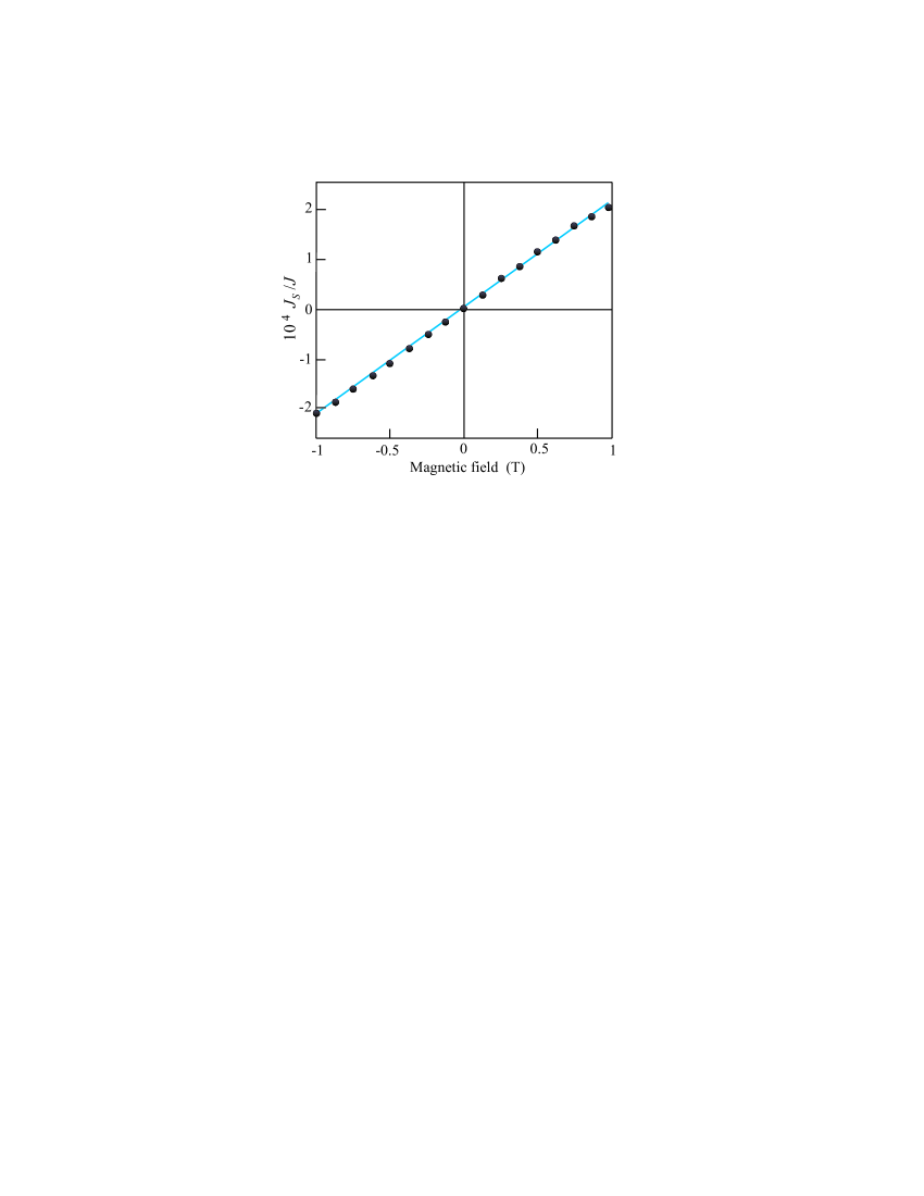
The spin-dependent component of the photocurrent was measured by a lock-in amplifier as the difference , where and are the photoemission currents for the excitation by right and left circularly polarized light, respectively. The light polarization was switched between the and states with a frequency of 1.5 kHz by means of a wide-aperture polarization modulator based on the linear electro-optic effect in Bi12SiO20.Alper19 The modulation of the polarization of the light beam was accompanied by a parasitic modulation of its intensity with a relative value of about . In order to exclude the influence of the intensity modulation on the results of the measurements, we took into account that SDP is an odd function of the magnetic field. To this end, the magnitude of was measured for two opposite directions of the magnetic field , and the value of SDP was determined as (the tilde over will be omitted in the text below). To justify the possibility of using this procedure, the linearity of on the magnetic field was tested. Figure 2 shows a typical magnetic field dependence measured at eV. At this photon energy, SDP caused by the jump in the factors gives the major contribution to the measured effect (see Fig. 3 and the text below). It is seen that in the investigated range of magnetic fields, is a linear function of the magnetic field, in accordance with phenomenological relation (1) and microscopic mechanism of the effect described in Sec. II. In the text below, basing on the linearity on , we present experimental data related to the maximal field T, which yield the highest signal to noise ratio.
IV Results and discussion
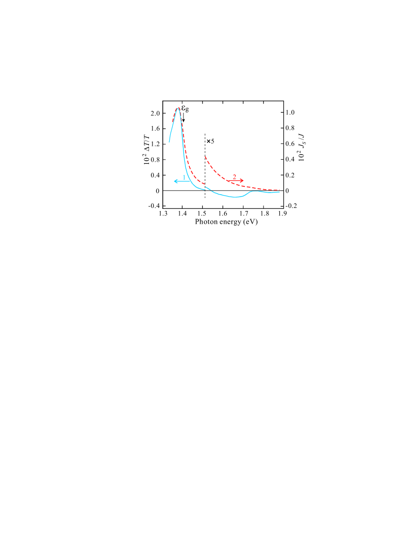
In addition to the spin-dependent photoemission caused by the jump in the electron factor at the semiconductor-vacuum interface, phenomenological equation (1) allows for the existence of bulk effects such as magnetically induced circular dichroism Seisyan20 ; Kaufmann21 and spin-dependent recombination Solomon22 ; Weisbuch23 ; Paget24 in the bulk of GaAs, which may also contribute to the experimentally measured values of . In GaAs, magnetically induced circular dichroism was previously studied for the impurity-related optical transitions below the band gap.Kaufmann21 To determine the magnitude of the circular dichroism for the above band gap optical transitions, we measured the relative change in the optical transmission of the GaAs photocathode under the change in the sign of light circular polarization . Figure 3 shows the spectrum of measured in the magnetic field T, as well as the spectrum of measured at T and V, when all emitted electrons are collected on the anode. From the comparison of the shapes of these two spectra, one can assume that circular dichroism yields the main contribution to SDP for photon energies near the band gap eV; however, this is not the fact for eV. It is also seen that for eV and 1.76 eV, dichroism vanishes, while is nonzero over the entire spectral range up to eV.
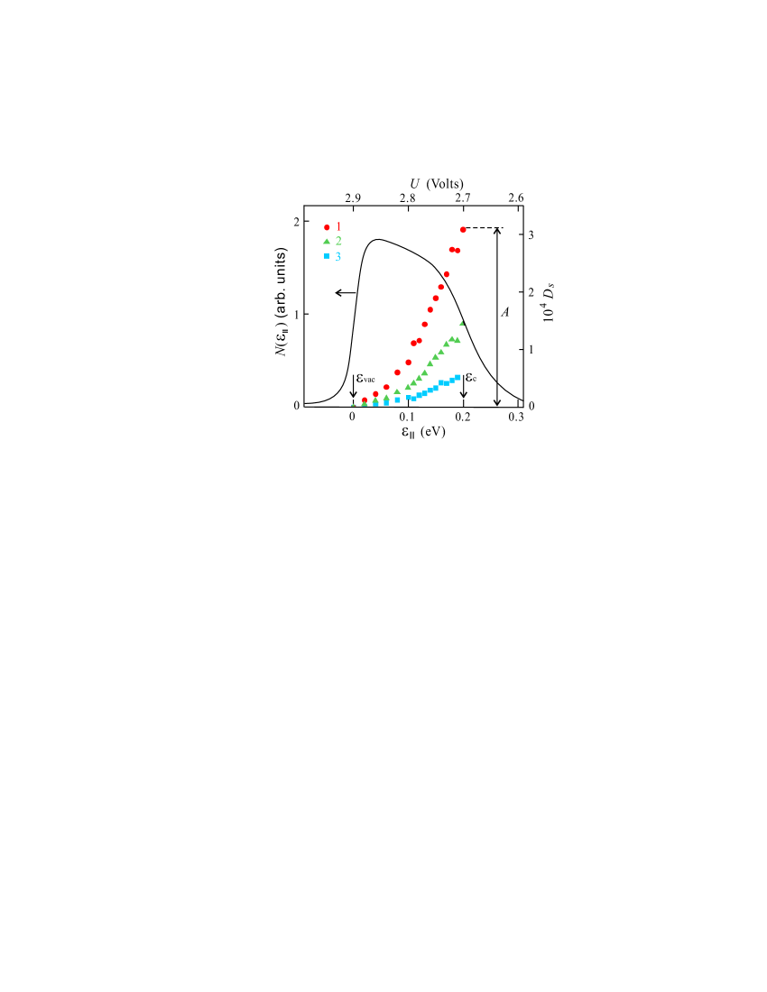
It was not possible to determine the contribution of magnetically induced spin-dependent recombination in the semiconductor bulk. Therefore, in order to extract the surface contribution to the spin-dependent photoemission, the procedure of measuring SDP was modified so that all bulk contributions, including dichroism and spin-dependent recombination in the bulk of GaAs, were subtracted from the measured values of . To this end, the magnitude of was measured at various voltages between the anode and cathode in the range of . The lower limit corresponds to an almost total cut-off of the photocurrent, when only a small part of electrons emitted into vacuum above the energy of the bottom of the conduction band in the bulk can reach the anode. The upper limit corresponds to a complete collection of all photoemitted electrons on the anode. To determine the limits of this range experimentally,Terek25 we measured the potential derivative of the photoemission current , which is proportional to the energy distribution function of emitted electrons (solid curve in Fig. 4). As seen in Fig. 4, the distribution function is bell shaped. The width of is equal to the magnitude of NEA;Terek8 in our case eV. The lower limit of the voltage range V corresponds to electrons which are emitted from the bottom of the conduction band without momentum and energy scattering with a kinetic energy in vacuum . The upper limit V corresponds to electrons at the vacuum level . In a previous work,Terek25 we described in detail the procedure for measuring the distribution function of electrons as well as for the energy calibration, which makes it possible to determine and to interlink the voltage scale with the energy scale and the position of the bottom of the conduction band in the semiconductor bulk.
In order to extract the surface contribution to SDP, we calculated the voltage-dependent part of the spin-dependent photocurrent. By varying the retarding voltage , we measured the SDP for different groups of electrons which undergo energy and momentum relaxation at the surface and are emitted into vacuum with longitudinal energies below the bottom of the conduction band in the bulk. For a zero surface spin-dependent contribution, the value of must be the same for different groups of scattered electrons. Therefore, the voltage-dependent part of SDP can be assigned to only the surface contribution because bulk contributions do not depend on .
The data points in Fig. 4 show the dependence measured at various photon energies . It is seen that at each the differential spin-dependent photocurrent is maximal for electrons emitted from the bottom of the conduction band and monotonically goes down with increasing , that is, with decreasing electron kinetic energy. It is also seen from Fig. 4 that the amplitude of variations in decreases with increasing photon energy, while the shapes of the dependences are similar. Figure 5 shows the scaled dependences measured at various . The scaling factors were fitted to minimize the difference between the measured dependences. It is seen that the shapes of all three dependences coincide with each other within the experimental accuracy. Thus, the shape of the energy dependence is indeed independent of the photon energy.
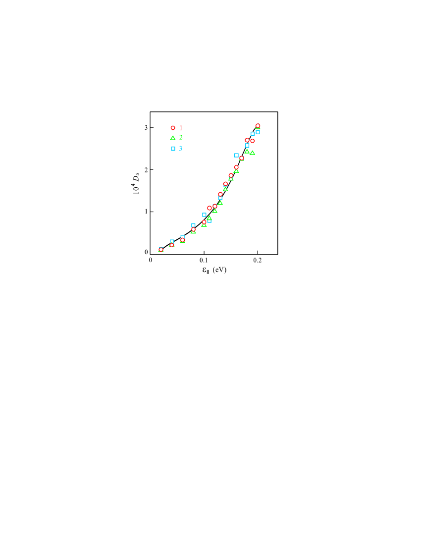
We compared the universal shape of the measured dependences to the calculation in the model of magnetically induced spin-dependent photoemission arising due to the jump in the factor at the GaAs(Cs,O)-vacuum interface. In this model the effective NEA and, consequently, the width of the energy distribution function of spin-polarized electrons vary by when the direction of the electron spin changes with respect to the magnetic field. The respective change in the current created by photoelectrons with mean spin is equal to . Thus, the voltage-dependent component of SDP can be expressed as follows:
| (2) |
This calculated dependence , which approximates the experimental dependences, is shown by the solid line in Fig. 5. For the calculation, we used the experimentally measured energy distribution function and the voltage dependence of the photoemission current obtained by numerically integrating this distribution. Taking into account a finite resolution meV of the measurements of the energy distribution function , Eq. (2) is valid for voltages . The value of the mean spin of photoemitted electrons was determined in the diffusion modelDzhioev26 from the spectral dependence of SDP amplitude (see Fig. 6). The value of the electron affinity modulation , which determines the amplitude of variations in SDP with varying , was a fitting parameter and found to be equal to 0.09 meV. The constant was determined so that the calculated value of coincides with the experimental value for . It is seen that the shape of the calculated dependence describes the experiment well. The fitting parameter meV should be compared with meV estimated from the known value of the electron factor on the bottom of the conduction band of GaAs. The agreement between the experimental and calculated values of may be considered as reasonably good, keeping in mind that photoelectrons acquire kinetic energy in the band bending region before emission, and this alters the effective factor due to its energy dependence.Pfeffer27 Moreover, according to Refs. Bell2, ; Korotkikh28, ; Orlov29, , in a semiconductor with the state of NEA, the photoemission occurs via electron capture to a two-dimensional sub-band in the band bending region and subsequent elastic or inelastic tunneling into vacuum through the potential barrier formed by the (Cs,O) layer. Therefore, the effective factor may be changed by the electron quantization,Ivchenko30 ; Kiselev31 ; Pfeffer32 as well as by the atomic structure of the GaAs(Cs,O) interface. The magnitude and energy dependence of SDP are also possibly influenced by the partial relaxation of the spin of electrons passing through the GaAs(Cs,O)-vacuum interface.Drouhin10 It is worth noting that along with the jump in the factor, a microscopic cause of the SDP at the surface may consist of spin-dependent recombination of photoelectrons on paramagnetic surface centers oriented by the magnetic field.Lepine33 However, spin-dependent recombination likely did not play a significant role in our experiment performed at room temperature.
The effect of spin-dependent photoemission can be used as a method for determining the spin diffusion length of electrons in semiconductors. The idea of this method can be explained as follows. Under photocathode illumination the spatial distribution of generated photoelectrons depends on the photon energy in accordance with the spectral dependence of the light absorption coefficient . Therefore, the photons with various energies generate electrons at various distances from the emitting surface. Due to electron spin relaxation in the course of the diffusion toward the emitting surface, the mean spin of emitted electrons depends on . As the amplitude of the surface contribution to SDP is proportional to , this leads to the spectral dependence of . The shape of this dependence is determined by the spin diffusion length of electrons.
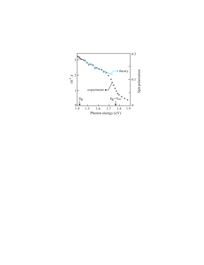
The measured spectrum of is shown in Fig. 6 by dots (left scale). It is seen that the amplitude of SDP decreases with increasing . The abrupt drop in near eV is due to the onset of optical interband transitions from the spin-orbit split valence band because these transitions generate electrons with spin opposite to the mean spin of electrons excited by near-band-gap optical transitions.Meier18 The gradual decrease in the SDP amplitude at photon energies is due to the dependence of the initial polarization of photogenerated electrons on (Ref. Meier18, ) and also due to spin relaxation of electrons during the diffusion towards the emitting surface.
In order to determine the spin diffusion length and the degree of spin polarization of photoemitted electrons, we compared the experimental dependence with the spectral dependence of the electron spin polarization calculated in the diffusion model Dzhioev26 in the spectral range of . The spectral dependence of the initial polarization of photogenerated electrons and spin depolarization in the process of diffusion toward the emitting surface were taken into account. The theoretical dependence is shown in Fig. 6 by the solid curve (the right scale). The following parameters of the AlGaAs/GaAs photocathode heterostructure were used for the calculation: the thickness of the active -GaAs layer, m; the electron diffusion length in the active layer, m; the recombination velocity between the -GaAs and buffer AlGaAs layers, cm/s; and the effective recombination velocity at the emitting surface, cm/s. The spin diffusion length was a fitting parameter. As the electron diffusion length and , the variations of the parameters (at m), (from to cm/s), and (in the range of cm/s) do not lead to significant changes in the calculated curve. The best fit value of the spin diffusion length was equal to m. The corresponding value of the spin polarization of photoemitted electrons generated by photons with energies near the band gap is equal to . The obtained value of the spin diffusion length is in good agreement with m reported by Dzhioev et al.Dzhioev26 The authors of Ref. Dzhioev26, studied spin polarization by the photoluminescence technique in a glass-bonded photocathode structure similar to that used in our photoemission experiment, with about the same value of doping level in the active -GaAs layer.
V Conclusions
Thus, it is experimentally found that in an external magnetic field the probability of electron emission from GaAs with the state of NEA into vacuum depends on the orientation of electron spin with respect to the direction of the field. This phenomenon stems from the jump in the electron factor on the semiconductor-vacuum interface. Due to this jump, the effective electron affinity of a photocathode depends on the mutual directions of the electron spin and magnetic field. This mechanism successfully describes the magnitude and energy dependence of SDP. A comparison of the measured and calculated spectra of the spin-dependent photoemission enabled us to determine the spin diffusion length in -GaAs and spin polarization of photoemitted electrons.
Acknowledgements.
This work was supported by the Russian Academy of Sciences (program ”Spin-dependent phenomena and spintronics”) and by the Russian Foundation for Basic Research (Grant No. 07-02-01005).References
- (1) Semiconductor Spintronics and Quantum Computation, edited by D. D. Awschalom, D. Loss, and N. Samarth (Springer, Berlin, 2002).
- (2) R. L. Bell, Negative Electron Affinity Devices (Clarendon, Oxford, 1973).
- (3) C. Cacho, Y. Lassailly, H.-J. Drouhin, G. Lampel, and J. Peretti, Phys. Rev. Lett. 88, 066601 (2002).
- (4) V. L. Alperovich, A. S. Terekhov, A. S. Jaroshevich, G. Lampel, Y. Lassailly, J. Peretti, N. Rougemaille, and T. Wirth, Nucl. Instrum. Methods Phys. Res. A 536, 302 (2005).
- (5) D. T. Pierce, R. J. Celotta, G.-G. Wang, W. N. Unertl, A. Galejs, C. E. Kuyatt, and S. R. Mielczarek, Rev. Sci. Instrum. 51, 478 (1980).
- (6) R. Prepost and T. Maruyama, Annu. Rev. Nucl. Part. Sci. 45, 41 (1995).
- (7) H.-J. Drouhin, C. Hermann, and G. Lampel, Phys. Rev. B 31, 3859 (1985).
- (8) A. S. Terekhov and D. A. Orlov, JETP Lett. 59, 864 (1994).
- (9) D. A. Orlov, M. Hoppe, U. Weigel, D. Schwalm, A. S. Terekhov, and A. Wolf, Appl. Phys. Lett. 78, 2721 (2001).
- (10) H.-J. Drouhin , C. Hermann, and G. Lampel, Phys. Rev. B. 31, 3872 (1985).
- (11) A. Voskoboynikov, S. S. Liu, and C. P. Lee, Phys. Rev. B 58, 15397 (1998).
- (12) V. I. Perel’, S. A. Tarasenko, I. N. Yassievich, S. D. Ganichev, V. V. Bel’kov, and W. Prettl, Phys. Rev. B 67, 201304(R) (2003).
- (13) S. A. Tarasenko, V. I. Perel’, and I. N. Yassievich, Phys. Rev. Lett. 93, 056601 (2004).
- (14) T. Gruber, M. Keim, R. Fiederling, G. Reuscher, W. Ossau, G. Schmidt, L. W. Molenkamp, and A. Waag, Appl. Phys. Lett. 78, 1101 (2001).
- (15) J. Fabian, I. Žutić, and S. Das Sarma, Phys. Rev. B 66, 165301 (2002).
- (16) D. A. Orlov, V. L. Alperovich, and A. S. Terekhov, JETP Lett. 83, 453 (2006).
- (17) C. Weisbuch and C. Hermann, Phys. Rev. B 15, 816 (1977).
- (18) Optical Orientation, Modern Problems in Condensed Matter Sciences Vol. 8, edited by F. Meier and B. P. Zakharchenya (North-Holland, Amsterdam, 1984/Nauka, Leningrad, 1989).
- (19) V. L. Alperovich, A. O. Minaev, S. P. Moshchenko, and A. S. Terekhov. Opt. Spectrosc. 65, 798 (1988).
- (20) R. P. Seisyan, Spectroscopy of Diamagnetic Excitons (Nauka, Moscow, 1984).
- (21) U. Kaufmann and J. Windscheif, Phys. Rev. B 38, 10060 (1988).
- (22) I. Solomon, J. Non-Cryst. Solids 35-36, 625 (1980).
- (23) C. Weisbuch and G. Lampel, Solid State Commun. 14, 141 (1974).
- (24) D. Paget, Phys. Rev. B 30, 931 (1984).
- (25) A. S. Terekhov and D. A. Orlov, SPIE Proc. 2550, 157 (1995).
- (26) R. I. Dzhioev, B. P. Zakharchenya, R. R. Ichkitidze, K. V. Kavokin, and P. E. Pak, Fiz. Tverd. Tela 35, 2821 (1993).
- (27) P. Pfeffer and W. Zawadzki, Phys. Rev. B 41, 1561 (1990).
- (28) V. L. Korotkikh, A. L. Musatov, and V. D. Shadrin, JETP Lett. 27, 616 (1978).
- (29) D. A. Orlov, V. E. Andreev, and A. S. Terekhov, JETP Lett. 71, 151 (2000).
- (30) E. L. Ivchenko and A. A. Kiselev, Sov. Phys. Semicond. 26, 827 (1992).
- (31) A. A. Kiselev, E. L. Ivchenko, and U. Rössler, Phys. Rev. B 58, 16353 (1998).
- (32) P. Pfeffer and W. Zawadzki, Phys. Rev. B 74, 115309 (2006).
- (33) D. Lepine, Phys. Rev. B 6, 436 (1972).