Resonant Energy Transfer from Organics to Quantum Dots and Carrier Multiplication
Abstract
It was shown in the recent experiments that the hybrid organic/inorganic resonant structures can provide a flexible materials platform aimed at the design of novel light emitting devices. The applications of hybrid structures for photovoltaic solar cell can also be useful. We pay attention in this note that the resonant energy transfer in hybrid structure from the organic thin layer to the semiconductor nanostructures can drastically increase the intensity of the free carrier generation. To demonstrate this idea we use the results of recently published paper by Zhang et al. [1] demonstrating the highly efficient resonance energy transfer from J-aggregates layer to semiconductor nanocrystals. It is known that the semiconductor nanocrystals with small energy gap represent a promising route to increased solar conversion in single–junction photovoltaic cells. We argue that the using of nanocrystals with small energy gap in the hybrid organic/inorganic structures similar to created in [1] can increase tens times the total intensity of carrier multiplication. The organic part in such hybrid structures will play a role of the peculiar organic concentrator of the light energy.
PACS Numbers: 71.35.Aa, 71.35.Gg, 78.67.Pt, 78.90+t.
Keywords: Excitons (Frenkel, Wannier-Mott), hybrid organic/inorganic structures, J-aggregates, Förster-like excitation transfer, carrier multiplication, solar cells
References
- [1] Q. Zhang et al., Nature Nanotechnology 2, 555 (2007)
- [2] V.M. Agranovich et al., J. Phys. Condens. Matter 10, 9369 (1997).
- [3] V.M. Agranovich, Hybrid Organic-Inorganic Nanostructures and Light-Matter Interaction, in: Problems of Condensed Matter Physics, Quantum coherence phenomena in electron–hole and coupled matter–light systems, edited by A.I. Ivanov and S.G. Tikhodeev, Clarendon Press, Oxford, 2008, pp. 24-42.
- [4] V.M. Agranovich et al., Synthetic Metals 1116 (1-3), 349 (2001).
- [5] M. Achemann et al., Nature (London) 429, 642 (2004).
- [6] G. Itskos et al., Phys. Rev. B 76, 035344 (2007).
- [7] S.Blumstengel et al., Phys. Rev. Lett. 97, 237401 (2006).
- [8] D.M.Basko et al., Phys. Rev. B 71, 165330 (2005).
- [9] A.J. Nozik, Physica E 73, 253318 (2002).
- [10] V.I. Klimov, Annual Review of Physical Chemistry 58, 635-673 (2007).
- [11] M.C. Beard et al., Nano Letters 7, 2506 (2007).
- [12] M. Born and E. Wolf, Principles of optics, Pergamon Press, Oxford, 1986.
1 Efficient Energy Transfer in Resonant
Organic/Inorganic
Nanostructures
Majority of commercial optoelectronic devices are built on the basis of inorganic or organic semiconductors, respectively, in light emitting devices, solar cells and nonlinear media. Crystalline inorganic semiconductors exhibit a good electronic transport with moderate optical cross–sections. Organic materials possess large optical oscillator strengths but are mostly limited to relatively low performance areas due to inferior mobility of charge carriers. A fundamentally new direction to overcome some of the limitations and liabilities of conventional material approaches while creating an entirely different class of multifunctional high performance optoelectronic materials is to exploit physical synergy in resonant organic-inorganic hybrid nanostructures. The most common form of exciton in an organic semiconductor is a Frenkel exciton, which is tightly localized on a single molecular site and moves as a unit through the molecules. On the other hand, the Wannier -Mott excitons found in inorganic semiconductors can span across hundreds of lattice unit cells. In resonant organic–inorganic structures the electronic excitations of the organic part (Frenkel excitons, strong excitonic transitions) and of the inorganic part (Wannier–Mott excitons, good transport, large nonlinearities) are energetically matched and coupled in a weak or strong coupling regime. The resonant nanostructures could thereby provide a flexible materials platform aimed at the design of novel optoelectronic devices exploiting specific assets of both their organic and inorganic constituents and exhibiting qualitatively new properties that would be absent in each class of the materials separately. The different properties of hybrid nanostructures, including properties of hybrid nanostructures in a weak and strong coupling regime and also in microcavity configuration, was discussed in many papers (see, for instance, review papers [2, 3] and references therein). In this note we discuss only out-of- microcavity hybrid nanostructures in weak coupling regime. For such structures is typical the possibility of fast and efficient non-radiative (Förster–like) excitation energy transfer between inorganic and organic nanostructures due to the pure electrostatic interaction.
This effect was suggested [4] as a new concept for light emitting devices where the electric pumping of excitations in the inorganic semiconductor quantum well (QW) would efficiently turn on the organic material luminescence for enhanced light emission from the material composite. Due to its Coulomb mechanism, the energy transfer is longer–ranged than direct charge transfer and only has a requirement of a reasonable exciton energy overlap between organic and inorganic semiconductor materials to create nanoscale interfaces with useful electromagnetic properties. Very recent experiments confirmed the possibility of this type of energy transfer between nanostructures. We have in mind, for example, the observation of efficient energy transfer between an inorganic (InGaN) QW and an adjacent layer of quantum dots (QDs) [5], between a (Ga, In)N/GaN QW to thin organic polyfluorene films [6], between ZnO QW to an organics (6T) or POPOP in [7]. In mentioned papers the observed coupling takes place between excitons within the hybrid composite. To fully exploit the non-radiative, electrostatic coupling between these different types of excitons, one must seek for materials with large exciton transition dipole moment and consequently with a large oscillator strength. These materials, as known, in the same time should exhibit a strong photon–matter interactions (strong absorption and short radiative life time of excitons). These properties help in the search of materials which can be used in constructing the resonant organic/inorganic nanostructures.
2 Förster-like Energy Transfer from Organics to Quantum Dots for Carrier Multiplication
The possibility of energy transfer from organics to quantum well was noted in consideration of interaction of quantum well excitations with a resonant localized excitation in organics [8]. Such process is opposite to energy transfer from quantum well (or quantum dot) to organic material which we considered above in the previous section. As we mentioned, such process can be used for the creation of a new type of the light emitting devices. The opposite process of electronic energy transfer from organic material to semiconductor nanostructure (quantum well or quantum dots) which we consider in this section can be interesting for a creation of a new type of solar cell. The same as under influence of photons this process also will result in creation of a free electron–hole pairs in inorganic nanostructure which in contrast to organic materials typically have a high mobility of carriers. Thus, in this case, the most complicated process for organic solar cells, the process of the transformation of the Frenkel exciton into the charge- transfer exciton with the subsequent charge separation does not appear at all. However, in many cases the energy pumped by organic nanostructure to inorganic one can be much larger that those pumped by photons from the same beam. We demonstrate this possibility considering as the model of hybrid structure the results of the recently published paper [1]. Using this paper we discuss the electronic energy transfer from organics to semiconductor nanocrystals (NCs)and its possible role in the process of charge multiplication. However, in contrast to NCS taken in [1] we propose to use NCs with small energy gap.
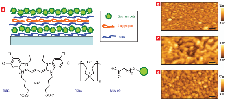
In the paper [1] the multilayer structure presented in Fig.1 has been investigated. The structure was obtained by layer -by- layer (LBL) assembly approach. Figure 1.a schematically shows the typical structure of the hybrid organic/inorganic (J-aggregate/QD) LBL films that was synthesized for the discussed study, along with the chemical structures of the constituents. In the hybrid film a single monolayer J-aggregate of cyanine dye (TDBC) was sandwiched between two monolayers of CdSe -ZnS core shell structured NCs (quantum dots), with polyelectrolyte (PDDA) acting as the ultrathin ”molecular glue”. Two types of hybrid films were considered in [1], one with NCs emission centered at 548 nm (referred to as film I) and the other at 653 nm (referred to as film II), thus providing contrasting cases of excitation coupling with respect to the fixed J-aggregate emission at 594 nm. Representative atomic force microscopy (AFM) images of hybrid film II and two additional NCs and J-aggregate reference films are shown in Fig. 1. b-d.
It was found for films II that resonance coupling of electronic excitations in J-aggregates with electronic excitations in the two monolayers of NCs can reach efficiencies of energy transfer from J-aggregates to NCs up to 98 percents at room temperature. This result can be especially interesting for properties of single-junction photovoltaic cells if in the structure similar to that presented in Fig. 1. instead of layers of CdSe-ZnS core shell structured NCs used in [1] to use NCs with small energy gap (PbSe or similar). Such NCs usually are used in the studies of the carrier multiplication, the effect which is the direct photogeneration of multiexcitons in NCs by single photons [9, 10, 11].
NCs contain approximately 100 to 10,000 atoms. Because of the strong spatial confinement of electronic wave functions and reduced electronic screening, the effects of carrier–carrier Coulomb interactions are greatly enhanced in NCs compared with those in bulk materials. These interactions open a highly efficient decay channel via Auger recombination and just a strong carrier- carrier interaction in NCs is responsible for carrier multiplication [9]. It is clear that the Förster resonant energy transfer (FRET) of electronic energy excitation with energy 2 - 4 eV from organic material to NCs with small energy gap of order of 0.5 eV in structures similar to presented in Fig. 1 also can give a carrier multiplication. However, this process can have a few interesting peculiarities in comparison with carrier multiplication under influence of photons of the same energy.
First of all a high efficiency of energy transfer from organic material to NCs can drastically increase the number of carriers in NCs, because the absorbtion of light by rather dense organic material can be much larger than the absorption of light by the system of separated NCs (in the case of structure created in [1] the absorption in organics is larger than the absorption of NCs system more than ten times, see Fig. 2 from [1]). One can expect that absorption of the NCs based on an equivalent bulk volume is very close to absorption of corresponding bulk semiconductor. However, the NCs have to be separated and the relatively small absorption of light by NCs is the result of a small density of NCs which cannot be larger than some critical value.
The second important feature of the carrier multiplication under the influence of energy transfer is the structure of electric field in the volume of NC. In the simplest approximation this field is created by transition dipole moment in organic molecules. This field even in spherical NCs is more inhomogeneous and non -spherical than created by plane wave of photon (see, for example, [12], Ch. XIII). It is clear that this asymmetry of the electric field could be responsible for change of the selection rules, determining the population of electron higher energy states in NC. This effect needs a careful analysis and is interesting because it can decrease the minimal energy of excitation which produces carrier multiplication. In the case, for example, of pumping of NCs (PbSe and PbS) by light this minimal energy is equal to the threefold energy gap [10, 11]. One can expect that for such NCs and with pumping of them by Förster–like energy transfer this threshold will be smaller.
Acknowledments
V. M. A. thanks Anton Malko and Yuri Gartstein for discussions. He is also thankful to Russian Foundation of Basic Research for partial support.