Hexagonal spiral growth in the absence of a substrate
Abstract
Experiments on the formation of spiraling hexagons (350 - 1000 nm in width) from a solution of nanoparticles are presented. Transmission electron microscopy images of the reaction products of chemically synthesized cadmium nanocrystals indicate that the birth of the hexagons proceeds without assistance from static screw or edge dislocatons, that is, they spiral without constraints provided by an underlying substrate. Instead, the apparent growth mechanism relies on what we believe is a dynamical dislocation identified as a dense aggregate of small nanocrystals that straddles the spiraling hexagon at the crystal surface. This nanocrystal bundle, which we term the “feeder”, also appears to release nanocrystals into the spiral during the growth process. TeX .
pacs:
61.46.Df, 61.46.Hkyear number number
LABEL:FirstPage1 LABEL:LastPage#1102
Crystals and their faceted faces are beautiful and remarkable especially when considering how their atomic constituents structurally organize. How do atoms in crystal growth processes ”know” when to turn left or right, or stop growing in a particular direction to pursue a new direction? When is a crystal a crystal and no longer a fluid?
The answers to these questions are difficult to address experimentally because of the challenges of catching atoms in the act of crystallizing.Yau However there are clues that allow one to confirm existing theories concerning the nature of the underlying growth mechanism. Take, for example, the case of screw dislocations. In 1949 Frank Frank1 had the insight that crystals emerge from the existence of screw dislocations that allow them to grow from stepped surfaces. This controversial claim was based on what Frank noticed as large discrepancies between experimental growth rates and the inability of two-dimensional nucleation theory to account for them. After much skeptism from the crystal field community Cahn , Frank’s theory was confirmed by the appearance of spiraling constructs on the surface of carborundum when decorated with minute amounts of silver and looking at the resulting refractory patterns.verma Thus, the concept of screw dislocations manifested by spiraling crystals was not only verified but also became the impetus to a new way of thinking about crystal growth mechanisms. And today this active area of research continues to find growth spirals in materials such as thin films of high temperature superconductors Gerber , metals Redinger , gallium nitride Strunk and organic materials such as pentacene Ruiz to name a few. Screw dislocations may even be responsible for supersolidity in 4He Chan as demonstrated by several theorists using Monte Carlo simulations. Troyer
If the crystal growth process advances without a substrate vinokur is it still possible to form faceted growth spirals? In this Letter we report experimental evidence which indicates that a substrate with screw (or edge) dislocations is not essential for hexagonal spiral crystals, at least not in two dimensions (2D). Surprisingly stable 2D spiral crystals can be produced by chemical synthesis techniques employed in the reduction of metallic salts. As will be addressed in this paper, these spirals appear to be governed by a dense aggregate of small particles believed to be two dimensional nuclei. This dense cluster intersects at the surface of the hexagonal spiral and possibly serves as a dynamical dislocation moving along the periphery of the hexagon and discharging particles into the spiral. Hereafter, we refer to this cluster as the ”feeder”. But before discussing the growth of 2D spiral crystals, the overall process of forming 2D hexagons is described.
Two dimensional cadmium hexagons were synthesized by reduction of cadmium acetate in a three neck flask with oleic acid and trioctylphosphine serving as ligands in the presence of a solvent (octyl ether or octadecene). Besides serving as a ligand, oleic acid, as the dominate player in these reactions, also helps reduce cadmium acetate, slow down the reaction, and control the shape of the resulting nanocrystals. Large concentrations of oleic acid, a very long chain organic molecule, prevent the formation of hexagons all together indicating that the competition between cadmium’s inclination to form hexagons is blocked by oleic acid’s polar and nonpolar composition. Since cadmium nanocrystals produced in these reactions are extremely nonpolar, its nonpolarity favors the large nonpolar portion of oleic acid while it is strongly repulsed by oleic acid’s polar end. Finally it should be emphasized that cadmium is a carcinogen, so careful handling must be carried out. (A detailed description of the synthesis will be published elsewhere.)
With the proper selection of reaction time, temperature, stirring speed and relative concentration between the precusor and ligands, hexagons and spiraling hexagons can be synthesized. Figure 1 shows the transmission electron microscopy (TEM) image for the case of transparent 2D hexagons containing both symmetric and antisymmetric shapes. These TEM images are prepared by pipeting a single drop of the toluene nanocrystal solution onto a TEM grid and imaging at 300 keV using a FEI Tecnai F30 instrument. Due to the thinness of these nanocrystals, the large surface area to volume ratio, and the fact that these nanocrystals are not isolated from one another makes them susceptible to bending forces. Evidence of this is manifested in the bend contours that are seen from Bragg diffraction effects shown as broad dark and light bands extending outwards from a central point. It is also possible to observe Moire patterns (shown in the inset) when two different crystalline hexagons lie on top of one another. In this inset, the top hexagon is partially folded over which creates bending contours discernible in the hexagon lying beneath.
Bulk cadmium, itself, has some interesting properties which might explain a few of the features presented here. Cadmium, a hexagonally closed packed (hcp) crystal, naturally likes to form hexagons as shown in Fig. 1; in addition, of all the hcp elements, it has the largest c/a ratio (1.886) Kittel (c is the length between equivalent basal planes and a is the distance between nearest neighbors within the hexagonal structure) and is thus far removed from the ideal hcp crystal 8/3 (=1.633) which refers to the closest possible stacking of spheres in a hexagonal lattice. This fact might explain why in these chemically synthesized nanocrystals only very flat, two dimensional crystals are formed.
Besides characterization by transmission electron microscropy (TEM), x-ray diffraction patterns on 12 different samples (not shown here) revealed a strong preferred orientation along the (002) direction parallel to the underlying glass substrate used for the measurement. This is consistent with earlier measurements on evaporative thin films of cadmium.Halder In the majority of x-ray diffraction results for these chemically produced cadmium nanocrystals, the (002) peak was the only peak in the diffraction spectra. It is important to note that these crystals were not susceptible to oxidation (no CdO diffraction peaks were observed in the x-rays results and there was no indication of the reddish tint of CdO in solution) which supports our hypothesis that the nonpolar portion of oleic acid is combining with the cadmium nanocrystals.
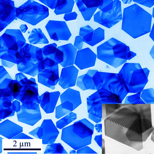
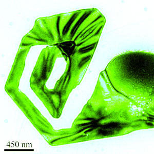
Figure 2 shows an TEM image of a single hexagonal spiral. While the segments of the spiral are well delineated and stable, there is also a large rounded body of mass at the end of the spiral. Also in the image there are clear patterns of dark and light colored fringes indicating the bending modes as the crystal forms and overlaps with itself. It is noteworthy that in the lower right of the crystal, the emerging bend is evident as dark black lines extend from a central region as the crystal begins to turn and form another segment of its six fold geometry. The separation of the segments could be due to oleic acid or simply empty space. As the nanocrystals were cleaned in various polar/nonpolar solvents before placing them in distilled toluene, the effect of cleaning may have removed the interior oleic acid which is what we believe keeps the separation between the segments of the hexagon when forming in solution. This configuration was the only one of its kind observed in TEM images produced from this particular reaction (although only a small portion of the reaction product was sampled).
Another reaction produced additional spiraling hexagons under slightly different conditions. In Figure 3, TEM images of 9 individual spiraling hexagons are shown. Again it should be emphasized that these were not the dominant configurations found in solution and were selected amongst other shapes which were not spiraling hexagons. In the TEM images of Figure 3, it is observed that there is a feeder attached to several spiraling hexagons. This asymmetric feeder appears to be responsible for the overall growth and resulting size of the nanocrystals. Although the nature of the feeder is still unclear, it is likely that it contains large numbers of loose two dimensional Cd nuclei that are free to move inside the spiral. It also appears to be responsible for the outermost edge of the spiral being perfectly straight, whereas the interior segments of some spirals seems to deviate from an ideal hexagonal geometry. Since the spirals are grown from inside out, it is possible that the interior slightly looses its posture as the crystals are swirling around in solution before the growth process is quenched.
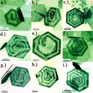
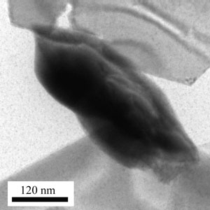
The feeder of Fig. 3i is enlarged in Fig. 4. In this expanded image, the feeder appears to be three dimensional with structure akin to an asymmetric hexagon.
There are notable exceptions to this apparent feeder as shown in the TEM images of Fig. 3 b & c. Here the spiraling hexagons are apparently feeding off non-spiraling hexagons. Since these are well developed spirals the dense feeder may have been present at an earlier stage of its growth.
The rounded mass feature that was a part of the spiraling hexagon shown in Fig. 2 is also evident in the images of Fig.3 a & e. These rounded features do not appear to be mechanically or artificially attached but rather appear to be an integral part of the hexagons like the one shown in Fig. 2. In Fig. 3e, the starting point, or head of the spiraling hexagon, is itself a hexagon. The rounded feature follows and is not at the end of the spiraling hexagon like the previous cases. The growth mechanism of this particular hexagon also does not appear to rely on a feeder or adjoining hexagon. However, it may be the case that the feeder was removed in the process of preparing the sample for TEM imaging.
The dimensionality of the spiraling hexagons is assumed to be two dimensional. This assumption is based on two key features observed in the TEM images of Figure 3. One is the electron transparency through spiraling hexagons, and the other is the appearance of bending modes that can span the breadth of the hexagons ( see for example Fig. 3g).
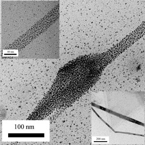
Is the distinctiveness of the spirals a consequence of thermal agitation by the electron beam used when imaging these structures? In Figure 5, TEM images of straight nanowires that do not spiral under identical imaging conditions are presented as counterexamples to spiraling hexagons. These cadmium nanowires were synthesized from a modified version of the same reaction that produced spirals and demonstrate that the beam of electrons from the TEM is not triggering the spiraling effect. The main physical difference between spiraling and nonspiraling hexagons is the presence of the feeder and chemically the main difference is the higher concentration of oleic acid used in the synthesis of the spiraling hexagons. The rounded protrusion seen in Figure 5 is likely a consequence of an early stage growth of the hexagonally shaped end that is a standard feature in the crystalline nanowires.
The possibility that this is a manifestation of pattern formation is now addressed. Experimentally the study of pattern formations in chemical reactions is most lucid in Belousov-Zhabotinsky (BZ) reactions Bel where spiral patterns spontaneously emerge.Jak The present situation is different from the Turing instabilityTur in that the spiraling pattern has six-fold symmetry. In addition much of the work on pattern formation is built around surface tension driven effects arising from a nondeformable liquid-gas interface. In most cases these effects involve a temperature gradient. This work addresses surface tension effects from liquid - solid interfaces using a colliodial technique in which there is a density gradient.
In summary, we presented experimental evidence for the formation of growth spirals with six-fold symmetry without the assistance of screw or edge dislocations from a substrate. These growth spirals were produced chemically and appear to be two dimensional. Spiraling in plane might be indicative of the presence of only two dimensional nanocrystals, the absence of a substrate, cadmium’s unusually large c/a ratio Kittel and the increased concentration of oleic acid used in the growth process. The main physical feature relevant to these spiraling hexagons is a feeder, either in the form of an aggregate of nanocrystals attached to the spiral or a neighboring hexagon. The position of the attached feeder could be interpreted as the same position that an analogous screw dislocation would have, however in this study it appears to be dynamical.
Future directions. Atomic force microscope analysis of the samples to obtain a height profile is necessary to confirm the dimensionality of these spirals and map height differences across a spiraling hexagon. Also these spiraling hexagons could possibly be exploited as a new type of metamaterial due to their unique configuration. Finally a detailed theoretical description needs to be established to address the features that are observed here.
Acknowledgements. The author thanks Heinrich Jaeger, Horst Strunk, John Royer, Robert Josephs,William Sweeney and Allen Goldman. This work was supported by the University of Chicago-Argonne Consortium for Nanoscience Research. The use of shared experimental facilities provided by the Chicago MRSEC is also gratefully acknowledged.
*Current address: The Physics Department and Center of Nanophysics and Advanced Materials at the University of Maryland, College Park. lladams@umd.edu
References
- (1) S.-T Yau and P. G. Vekilov, Nature 406, 494 (2000).
- (2) W. Burton, N. Carbrera, F. C. Frank, Nature 163, 398 (1949);W. K. Burton, N. Carbrera, and F. C. Frank, Philos. Trans. R. Soc. London A 243 (1951).
- (3) R. W. Cahn, The Coming of Material Science, Elsevier, Oxford, (2001).
- (4) A. R. Verma and S. Amelinckx, Nature 167, 939 (1951).
- (5) C. Gerber et al., Nature 350, 279 (1991); M. Hawley, I. D. Raistrick, J. G. Beery and R. J. Houlton, Science 251, 1587 (1991).
- (6) M. Ranganathan et al., Phys. Rev. Lett. 95, 225505 (2005); Redinger et al., preprint, cond-mat0709.2327 (2007).
- (7) Y. Cui and L. Li, Phys. Rev. B 66, 155330 (2002); L. Lymperakis et al., Phys. Rev. Lett. 93, 196401 (2004).
- (8) R. Ruiz et al., Chem. Mater. 14, 4497 (2004).
- (9) E. Kim and M. H. W. Chan, Nature 427, 225 (2004); Science 305, 1941 (2004).
- (10) M. Boninsegni, A. B. Kuklov, L. Pollet, N. V. Prokofev, B. V. Svistunov, and M. Troyer, Phys. Rev. Lett. 99, 035301 (2007).
- (11) I. S. Aranson, A. R. Bishop, I. Daruka and V. M. Vinokur, Phys. Rev. Lett. 80, 1770 (1998).
- (12) C. Kittel, Introduction to Solid State Physics, 7th edition, John Wiley and Sons, New York (1996).
- (13) N. C. Halder, M. Pita and P. L. Li, Surface Science 86, 200 (1979).
- (14) Belousov, B. P., Collection of Short Papers on Radiation Medicine, Medgiz, Moscow (1959); Zhabotinsky, A. M., Proc. Acad. Sci. USSR 157, 392 (1964).
- (15) S. Jakbith, H. H. Rotermund, W. Engel, A. von Oertzen, and G. Ertl, Phys. Rev. Lett. 65, 3013 (1990).
- (16) Turing, A. M., Philos. Trans. R. Soc. London B 237, 37 (1952).