Phase coherent transport in (Ga,Mn)As
Abstract
Quantum interference effects and resulting quantum corrections of the conductivity have been intensively studied in disordered conductors over the last decades. The knowledge of phase coherence lengths and underlying dephasing mechanisms are crucial to understand quantum corrections to the resistivity in the different material systems. Due to the internal magnetic field and the associated breaking of time-reversal symmetry quantum interference effects in ferromagnetic materials have been scarcely explored. Below we describe the investigation of phase coherent transport phenomena in the newly discovered ferromagnetic semiconductor (Ga,Mn)As. We explore universal conductance fluctuations in mesoscopic (Ga,Mn)As wires and rings, the Aharonov-Bohm effect in nanoscale rings and weak localization in arrays of wires, made of the ferromagnetic semiconductor material. The experiments allow to probe the phase coherence length and the spin flip length as well as the temperature dependence of dephasing.
pacs:
72.15.Rn, 75.50.Pp, 73.63.-b1 Introduction
The discovery of the ferromagnetic III-V semiconductor materials (In,Mn)As [1] and (Ga,Mn)As [2] has generated a lot of interest as these materials combine ferromagnetic properties, typical for metals, with the versatility of semiconductors (for a review see e.g. [3, 4, 5, 6, 7]). This allows, e.g., to control ferromagnetism by electric fields thus opening new prospects for application and fundamental research [8]. The Mn atoms in the III-V host are not only responsible for the ferromagnetism but also act as acceptors such that, at sufficiently high Mn-concentration, (Ga,Mn)As is a degenerate p-type semiconductor [9]. The ferromagnetic order of the Mn magnetic moments is mediated by holes via the Ruderman-Kittel-Kasuya-Yosida (RKKY) interaction [10]. By now ferromagnetism in (Ga,Mn)As is well understood, allowing to predict Curie temperatures [11], magnetocrystalline anisotropies [12] as well as the anisotropic magnetoresistance effect [13]. In this respect (Ga,Mn)As is one of the best understood ferromagnetic materials at all [14] and hence suitable as a model system to study quantum corrections to the conductivity in ferromagnets. The quest to increase the Curie temperature in (Ga,Mn)As towards room temperature has led to a thorough investigation of the material properties (see, e.g. [15] and references therein). By annealing (Ga,Mn)As sheets or by incorporating them into sophisticated layered arrangements the Curie temperature was increased up to 173 K [16, 17] and 250 K with Mn-doping [18], respectively. Despite the high crystalline quality of the material (Ga,Mn)As is a quite disordered conductor on the verge of the metal-insulator transition (MIT). For Mn concentrations on the metallic side of the MIT the typical mean free path of the holes is a few lattice constants. Hence it was until recently an open issue whether quantum effects like Aharonov-Bohm (AB) oscillations, universal conductance fluctuations (UCF) or weak localization (WL) can be observed in this class of materials. Accordingly the phase coherence length and the corresponding dephasing mechanisms which govern quantum mechanical interference phenomena in ferromagnetic semiconductors were unknown. Apart from being a fundamental material parameter this information is needed to design more sophisticated layered structures from ferromagnetic semiconductors. Examples are resonant tunneling diodes or other interference devices which rely on the electrons’ wave nature. Apart from the question on the relevant phase coherence lengths, quantum corrections to the resistance like weak localization are suppressed by a sufficiently strong perpendicular magnetic field [19]. Hence the question arises whether such effects can be observed at all in ferromagnets which have an intrinsic magnetic induction. Therefore, the advent of the new ferromagnetic semiconductor material (Ga,Mn)As with significantly smaller internal field compared to conventional ferromagnets offered a new opportunity to address such questions.
Below we first describe experiments to explore universal conductance fluctuations in (Ga,Mn)As nanowires to get knowledge of the relevant dephasing length and the main phase breaking mechanism. We show below periodic conductance oscillations in (Ga,Mn)As nanoscale rings to prove phase coherent transport by the Aharonov-Bohm effect. The last part of this manuscript describes weak localization experiments in arrays of (Ga,Mn)As nanowires, where aperiodic conductance fluctuations are suppressed by ensemble averaging.
2 Sample preparation and measurement technique
| Sample | w1 | w2 | w3 | w4 | w5 | r1 | r1a | r2 | r3 | a1 | a1a | a2 |
| (nm) | 100 | 200 | 300 | 800 | 370 | - | - | - | - | 7500 | 7500 | 7500 |
| (nm) | 20 | 20 | 20 | 20 | 35 | 30 | 30 | 18 | 30 | 42 | 42 | 35 |
| (nm) | 50 | 50 | 50 | 50 | 42 | 50 | 50 | 42 | 42 | 42 | 42 | 42 |
| 1 | 1 | 1 | 1 | 1 | - | - | - | - | 25 | 25 | 12 | |
| (nm) | - | - | - | - | - | 120-180 | 120-180 | 120-155 | 160-220 | - | - | - |
| (h) | 0 | 0 | 0 | 0 | 0 | 0 | 12 | 51 | 51 | 0 | 51 | 0 |
| (K) | 55 | 55 | 55 | 55 | 90 | ? | 100 | 150 | 150 | 90 | 150 | 90 |
| (m) | 1.8 | 1.8 | 1.8 | 1.8 | 3.5 | 2.7 | 3.1 | 9.3 | 9.3 | 3.8 | 9.3 | 3.8 |
| (m2/s) | 4.8 | 4.8 | 4.8 | 4.8 | 8 | 2.5 | 4.4 | 12 | 12 | 8 | 12 | 8 |
| (nm) | 110 | 95 | 90 | 155 | 135 | 125 | 160 | 130 | 130 | 150 | 190 | 160 |
| (ps) | 270 | 195 | 170 | 500 | 175 | 625 | 600 | 140 | 140 | 280 | 300 | 320 |
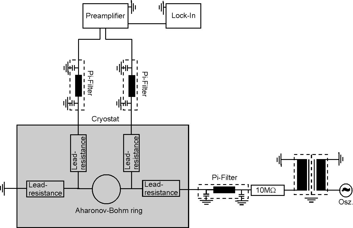
To explore phase coherent phenomena in (Ga,Mn)As we fabricated nanoscale wires, rings and arrays of wires, connected in parallel, from several wafers, always containing a ferromagnetic (Ga,Mn)As layer on top of a semi-insulating GaAs (100) substrate [20]. The magnetic easy axis of all investigated wafers was in plane. The relevant parameters of the samples used are listed in table 1. All investigated samples were fabricated using electron-beam-lithography (a Zeiss scanning electron microscope controlled by a nanonic pattern generator) and dry etching techniques. Ohmic contacts to the samples were made by thermal evaporation of Au and lift-off after brief in-situ ion beam etching for removing the native oxide layer of (Ga,Mn)As. The measurements were performed in a toploading dilution refrigerator (a Oxford Kelvinox TLM), equipped with a 19 T magnet, by standard four probe lock-in technique. The temperature regime accessible with this cryostat system ranges from 1 K to 15 mK. To avoid the heating of charge carriers at very low temperatures careful wiring, shielding and the use of low excitation currents (down to 10 pA) were crucial. Without such measures quantum interference effects in (Ga,Mn)As can not be observed. The schematic experimental set-up is shown in figure 1. As we observe no saturation of the signals for the different effects (UCF, AB-oscillations and WL) at the lowest temperatures we assume that the effective electron temperature is in equilibrium with the bath temperature even at temperatures as low as 20 mK.
In the experiments described below the wires can be treated as quasi one dimensional in the context of phase coherent transport. The relevant parameters for the one dimensional treatment are the phase breaking length and the thermal diffusion length . The phase breaking length gives the length scale an electron can travel without loosing phase information. The thermal diffusion length gives the length scale on which the thermal broadening of energies around the Fermi surface leads to a smearing of the interference effects. The thermal length is given by . Here is the diffusion constant given by , with the Fermi velocity and the momentum relaxation time . So our samples can be treated as quasi one dimensional as long as their width (in our experiments ranging from 18 nm to 42 nm) and thickness (ranging from 42 nm to 50 nm) are smaller than and . The thermal diffusion length of our samples is nm at 20 mK. Below we show that the dephasing length in our samples ranges between 100 nm and 200 nm at 20 mK.
As we deal here with ferromagnetic material the actual value of the magnetic field inside the material requires some attention. In the experiments described below the external magnetic field is always aligned along the growth direction of the (Ga,Mn)As structures, denoted as z-direction. Taking the external magnetic field along this z-direction, the magnetic field inside the (Ga,Mn)As is given by where is the magnetic polarization in z-direction and is the corresponding demagnetization factor. In case of a two dimensional ferromagnetic film, and internal and external field (in z-direction) are identical. In case of wires, explored here, the demagnetization factors are approximated by using cigar shaped ellipsoids with their long axis along the wire axis and the short axes corresponding to wire width/thickness [21]. For aspect ratios relevant here, i.e., a wire length of order 1 m (in x-direction) and wire cross sections of about 40 nm we obtain for the demagnetization factors and . Hence the internal field is . The maximum value of is given by the saturation magnetization of (Ga,Mn)As. Maximum values of our samples’ saturation magnetization are 30 emu/cm3 which translates in SI-system into values of 40 mT (see e.g. [5]). This means that the maximum difference between the externally applied field and the field inside the material is about 20 mT. The difference between and is practically zero at and at most 20 mT at the saturation field. This is only a small correction of the external field in the sense that the difference between internal and external field would hardly be noticeable on the magnetic field axes displayed below. We hence use in the following that .
3 Universal conductance fluctuations in (Ga,Mn)As wires and rings
One of the most straight forward methods of measuring the phase coherence length and its temperature dependency relies on measurements of universal conductance fluctuations in a single mesoscopic wire. Universal conductance fluctuations stem from interference of partial electron (hole) waves, scattered in a disordered mesoscopic conductor ([22] and references therein). If the wire is smaller than in all three spatial dimensions the fluctuation amplitude , where the bracket denotes averaging over [23]. The amplitude of these fluctuations gets, in contrast to AB oscillations, not exponentially damped once the wire length exceeds the dephasing length, but attenuated by a power law [23]:
| (1) |
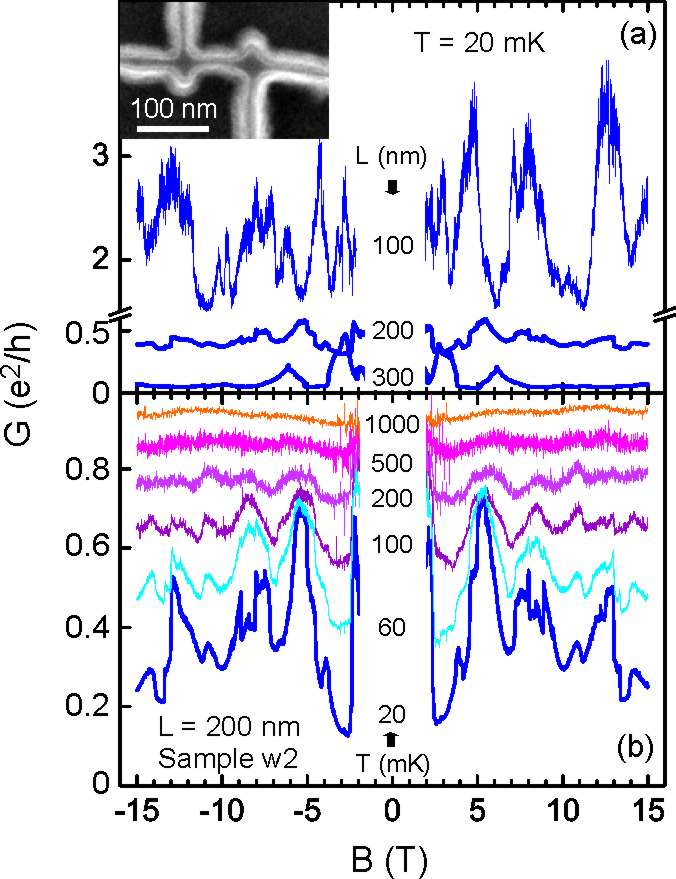
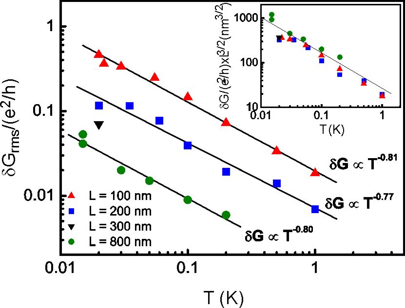
Here, is the wire length and is a constant, with a value close to or smaller than unity, depending, e.g., on the strength of spin-orbit coupling [24] and the applied magnetic field [23]. Equation (1), describing the fluctuation amplitude of one-dimensional (1D) conductors is applicable to extract the phase coherence length as long as is larger than the width and the thickness of the wire, and if the thermal diffusion length is larger than [23]: . Also the temperature dependency of the dephasing length can be extracted by measuring the temperature dependence of the fluctuation amplitude as is . To investigate UCFs in (Ga,Mn)As we fabricated individual nanowires with lengths between 100 nm and 800 nm and measured their resistance in a perpendicularly applied magnetic field . The relevant parameters of the wires, labeled w1-w4, are given in table 1. The conductance was obtained by inverting the resistance: . In figure 2a the conductance of three wires having a length of 100 nm, 200 nm and 300 nm, respectively, is plotted as a function of the perpendicularly applied magnetic field at 20 mK. Here, we focus on the high field region ( T) where the magnetization is saturated and aligned along the external magnetic field. For all three wires aperiodic, well reproducible conductance fluctuations are visible [25]. With increasing wire length not only the conductance of the wires decreases but also the amplitude of the conductance fluctuations drops, showing that at least the 200 nm and 300 nm long wires are longer than the dephasing length . The fluctuation amplitude measured in the 100 nm wire is 0.5 e2/h. Depending on the exact value of the prefactor in equation (1) the dephasing length is close to the wire length of 100 nm at 20 mK. To investigate the temperature dependency of the dephasing length we measured the conductance fluctuations of the wires at different temperatures. The magnetoconductance trace of wire w2 is displayed in figure 2b for different temperatures between 20 mK and 1 K. With increasing temperature the amplitude of the conductance fluctuations is decreasing until they disappear above 200 mK. Plotting the amplitude of the conductance fluctuations versus temperature in a log-log-plot (figure 3) gives a power law for the temperature dependence of the conductance fluctuations: for the 200 nm long wire w2 we obtain . This temperature dependency is similar for all investigated wires with an exponent between -0.77 and -0.81, approximated in the following by -3/4. Assuming a temperature independent prefactor we arrive at the temperature dependency of the dephasing length: . In case is smaller than the same temperature dependency of results. Instead of equation (1), with has to be used [23]. Doing so we again arrive at . The inset of figure 3 shows the amplitude of the conductance fluctuations normalized by the wire length. As all investigated samples lie on one straight line the expected length scaling of UCF, given by equation (1), is experimentally confirmed.
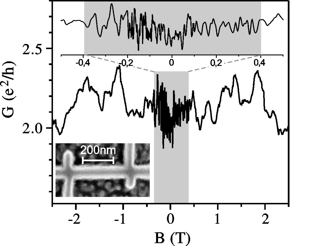
Before discussing this temperature dependence in more detail we address the conductance fluctuations in the low field regime, excluded in the discussion of figure 2. Corresponding data, taken from sample w5 are shown in figure 4. The magnetic field scale on which the conductance fluctuates is much shorter in the low- regime. The grey shaded area in figure 4 corresponds to the magnetic field range where the anisotropic magnetoresistance effect is observed, i.e., the -range where the magnetization is rotated from an in-plane to an out-of-plane orientation by the externally applied magnetic field. The correlation field of the conductance fluctuations is strikingly different in the low and high field regime. Similar behavior was observed in previous experiments on samples with in-plane easy axis [25, 26] and ad hoc ascribed to the formation of domain walls [26]. As in the low field regime the magnetic configuration is continuously changed by the external field, the scattering configuration is altered and the correlation field, which can also be used to extract the phase coherence length [23, 25], is not any more a well defined quantity. The phase coherence length extracted from the amplitude of the conductance fluctuations is, within experimental error, the same for low and high-field fluctuations.
The temperature dependency of the dephasing length has been confirmed by others, also investigating universal conductance fluctuations in (Ga,Mn)As nanowires [26]. Such a relatively weak temperature dependency for the dephasing length is typical for electron-electron scattering as dominating source of dephasing. In case of electron-phonon scattering or electron-magnon scattering one would expect a stronger temperature dependency of [27, 28]: . At low temperatures and reduced dimension electron-electron scattering with small energy transfer, the so called Nyquist scattering, becomes more effective, leading to [29]. However this temperature dependency doesn’t describe our results correctly. A possible candidate for dephasing in (Ga,Mn)As nanowires might be critical electron-electron scattering, describing dephasing in a highly disordered metal near the metal insulator transition [30]. The corresponding phase coherence length depends like on temperature. This is in accord with our results, but the calculations were done for a 3D system. Hence the detailed microscopic origin of dephasing in (Ga,Mn)As wires is still an open issue.
To probe whether electron-electron scattering is the main source of dephasing we investigated universal conductance fluctuations under non equilibrium conditions, meaning that the effective electron temperature is higher than the lattice temperature. To control the effective electron temperature the applied excitation current has been varied. Below we assume that even for our highest excitation currents of 8 nA the lattice temperature is not increased. This current corresponds to a voltage drop of 67 V across the sample and a heating power of W. The cooling power of our dilution refrigerator at 40 mK, on the other hand, is approx. 50 W which is 8 orders of magnitude higher.
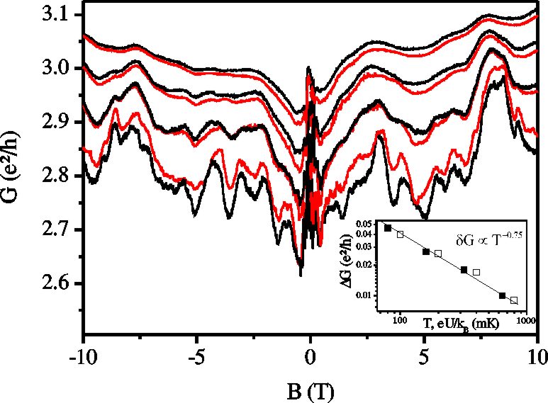
The sample is located in the 3He-4He mixture, so that thermal coupling should be sufficient to keep the lattice in equilibrium with the bath temperature. Figure 5 displays universal conductance fluctuations in a ring with a diameter of 150 nm (sample r1a in table 1). The conductance of this ring didn’t exhibit periodic conductance oscillations due to the Aharonov-Bohm effect, but only aperiodic conductance fluctuations, similar to the ones observed in wires. In figure 5 the fluctuations are successively suppressed by increasing either temperature or current. In one experiment the bath temperature was varied from 80 mK to 640 mK (black lines from bottom to top), while the excitation current was kept at a value where the effective electron temperature is still in equilibrium with the bath temperature (200 pA at 80 mK, 500 pA at 160 mK and 320 mK, and 1 nA at 640 mK. For comparison: 1 nA corresponds here to a voltage drop of 9.5 V across the sample, equivalent to mK). In this regime, the conductance fluctuations do not depend on the excitation current as long as the hole gas and the lattice are in equilibrium. Then we varied the excitation current, at a fixed bath temperature of 40 mK, from 1 nA to 8 nA (red lines from bottom to top). In that case the fluctuation amplitude is depending on the excitation current. As one can see in figure 5 the black and red traces lie quite well on top of each other. Thus we arrive at the same experimental result in two ways, first by increasing the bath temperature and secondly by raising the excitation current. Since the excitation current can’t change the lattice temperature, as argued above, the observed dephasing can’t depend on the lattice temperature. This means that electron-phonon and electron-magnon scattering can be excluded as source of dephasing. This is also consistent with the temperature dependency of the dephasing length, discussed above. The inset of figure 5 shows the average amplitude of the conductance fluctuations in figure 5, both as a function of the bath temperature (solid symbols) and the applied voltage in units of (open symbols), respectively. Both traces display the same slope and lie above each other. This suggest a linear correlation of effective temperature and applied voltage across. Such a linear dependence is only expected if the lattice is decoupled from the electrons [31] and if the effective electron temperature is given by . The dominating parameter for dephasing in the low temperature regime is hence the effective electron temperature and electron-electron scattering is the most likely source of dephasing.
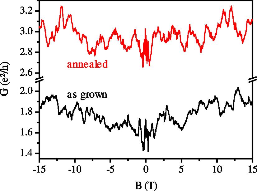
Low temperature annealing of (Ga,Mn)As causes an out diffusion of Mn ions which occupy interstitial lattice sites, act as double donors and couple antiferromagnetically to Mn ions on regular Ga-sites. So low temperature annealing increases the carrier concentration, the Curie temperature and the total magnetic moment of the samples [16]. Has such low temperature annealing of the samples an influence on the phase coherence length? In nonmagnetic metals magnetic impurities strongly reduce the phase coherence length [32]. This poses the question whether Mn interstitials have a similar effect on the dephasing length in (Ga,Mn)As, as they increase the magnetic disorder due to their random distribution. In order to look for effects of low temperature annealing we measured the conductance of a 150 nm diameter ring at 20 mK before (r1) and after annealing (r1a). The corresponding magnetoconductance traces are shown in figure 6 before (black line) and after annealing (red line). As expected the conductance increased significantly after annealing (here by a factor of approx. 2). While the amplitude of the conductance fluctuations is 0.055 e2/h before and 0.080 e2/h after annealing, the corresponding dephasing length, determined by equation (1), is increased by 30 % after annealing. Calculating the dephasing time we find that the dephasing time does not change after annealing. While increases, also the diffusion constant increases by about 75 % since both, the Fermi velocity (increased hole density) and the momentum relaxation time get larger. This means that the dephasing time is essentially not affected by low temperature annealing. The change in coherence length is only due to the change of the diffusion constant. If electron-electron interaction is the source of dephasing one would expect that depends on the carrier concentration. Since in our experiment the change in carrier density was only 15 % the dependency could not be resolved. The main difference of the Mn interstitials in (Ga,Mn)As compared to magnetic impurities in normal metal is the coupling strength. In normal metals the magnetic impurities are uncoupled above the Kondo-temperature and a spin-flip process is energetically accessible for the electrons, leading to a loss of phase information [33]. In (Ga,Mn)As the Mn interstitials are coupled quite strongly [14] and a spin-flip process is not possible. This explains why low temperature annealing does not increase the dephasing time, but only increases the dephasing length by an increase of the diffusion constant.
Spin-orbit (SO) interaction plays an important role in the valence band of (Ga,Mn)As and hence also has an effect on the analysis of UCFs. In equation (1) SO-interaction was not taken into account. Chandrasekhar et al. pointed out that the presence of spin-dependent scattering affects the amplitude of the conductance fluctuations [24]. The amplitude of the conductance fluctuations, determined by equation (1), depends on the ratio of phase coherence length and spin orbit lengths . With increasing the amplitude of the UCFs gets reduced. This means that in the presence of spin orbit interaction the phase coherence length gets larger for a given value of the UCF amplitude. To determine the corresponding factor requires knowledge of the spin-orbit length which can be extracted from weak-antilocalization correction. After we have extracted from weak localization experiments, discussed below, we return to this point again.
4 Aharanov-Bohm effect in (Ga,Mn)As rings
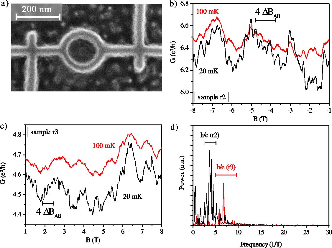
A quite prominent manifestation of phase coherence in mesoscopic conductors is the so called Aharonov-Bohm (AB) effect. In a ring geometry a wave-packet is split into two partial waves propagating along the upper and lower half of the ring perimeter and interfering at the ”exit”. The phase of the partial waves can be tuned by a perpendicular magnetic field so that, as a function of magnetic field strength, constructive and destructive interference of the partial waves can be adjusted. At sufficiently low temperatures the conductance across the ring displays periodic oscillations with a period , were is the area enclosed by the ring and is the flux quantum h/e. Periodic Aharonov-Bohm oscillations have been observed over the last decades in normal metals [34] and in low dimensional electron and hole systems, e.g. [35, 36]. However, the observation of AB-oscillations in ferromagnetic ring-structures is even more challenging and until quite recently it was unclear whether AB-effects can be observed at all in ferromagnets. First observation of AB effects have been reported in FeNi rings in the year 2002 [37]. Measuring the AB effect in (Ga,Mn)As-rings requires that the phase of a wave packet is preserved while traversing the ring. With increasing ring radius the amplitude is damped exponentially, exp [34]. Additionally an aspect ratio close to one (ratio of inner and outer radius of the ring) is needed to avoid smearing of the interference pattern. In (Ga,Mn)As the phase coherence length is about 100 nm at 20 mK. Hence AB oscillation should be visible in rings with diameters of about 100 nm to 200 nm. The conductances of the rings r1 and r1a, discussed above in figure 5 and 6 display no clear AB oscillations. In an attempt to resolve AB-type of oscillations the ring diameter was further reduced to a diameter of only 100 nm [25]. Corresponding magnetoconductance data of this ring clearly containing a contribution of the AB effect, are published in Ref. [25]. However, the associated Fourier spectrum is less clear as it displays no clear peak. One reason for this is the relatively bad aspect ratio of the ring causing a broadening of the Fourier peak. In an attemp to resolve AB oscillations we tried to increase the phase coherence length by increasing the diffusion constant of the (Ga,Mn)As material. We found the maximum diffusion constant of m2/Vs in an optimally annealed wafer containing approx. 5-6 % manganese and having a Curie temperature of 150 K. From this wafer we fabricated a ring with an inner diameter of 120 nm and an outer diameter of 155 nm (sample r2 in table 1). A corresponding electron micrograph is shown in figure 7a. The magnetoconductance of this ring is displayed in figure 7b. At a temperature of 20 mK well pronounced periodic oscillations emerge from the background with a period mT - 370 mT expected for the ring geometry. Also in the Fourier spectra a clear peak is visible at approx. 3.7 T-1 (see figure 7d, black trace). The aperiodic conductance fluctuations in the magnetoconductance arise, as in wires, from interference effects in the individual ring arms. These fluctuations are superimposed on the periodic AB conductance oscillations. From the amplitude of the oscillations we can estimate a phase coherence length of nm by using [34, 38]:
| (2) |
By increasing the temperature to 100 mK these periodic oscillations disappear. This strong sensitivity on temperature is a consequence of the temperature dependency of the phase coherence length and the exponential damping of the oscillations. To prove the dependence of the period on the ring diameter, i.e. the enclosed magnetic flux, we fabricated a ring, labeled r3, with an average diameter of 190 nm. Magnetoconductance data of this ring in a perpendicular applied magnetic field are shown in figure 7c. At 20 mK periodic AB oscillations are again visible but the amplitude is much smaller than the ones observed in the smaller ring. This is expected from the exponential suppression. Here the value of is again nm. The Fourier spectra in figure 7d (red trace) shows a peak at approx. 6.8 T-1 which is in very good agreement with the expected value between 4.8 T-1 and 9.1 T-1. While the lower value corresponds to the value of the inner diameter, the higher one is extracted from the flux through the outer diameter. Also in this ring the AB-oscillations are gone at 100 mK. A contribution of the first harmonic of the Aharonov-Bohm effect, with a period of h/2e, could not be observed in any of the rings investigated. The value of the dephasing length extracted from the Aharonov-Bohm oscillations is nm for both samples (sample r2 and r3) and thus consistent with the value extracted from the universal conductance fluctuations.
5 Weak localization and weak anti-localization in (Ga,Mn)As wire arrays
The effect of weak localization [19] belongs to the class of so called time reversed interference effects. Scattered partial waves of particles on time-reversed closed paths interfere constructively, causing an enhanced probability of backscattering which decreases the conductance. A perpendicular magnetic field destroys the constructive interference and hence the quantum mechanical correction to the conductivity and the resistance returns within a characteristic magnetic field scale towards the Drude value. The resulting negative magnetoresistance is the characteristic hallmark of weak localization. As the maximum area of the closed loops which contribute to weak localization is limited by the phase coherence length, fits of the WL-magnetoresistance provide another means to extract the phase coherence length. In the presence of spin-orbit interaction, the spin part of the wave function needs also to be taken into account.
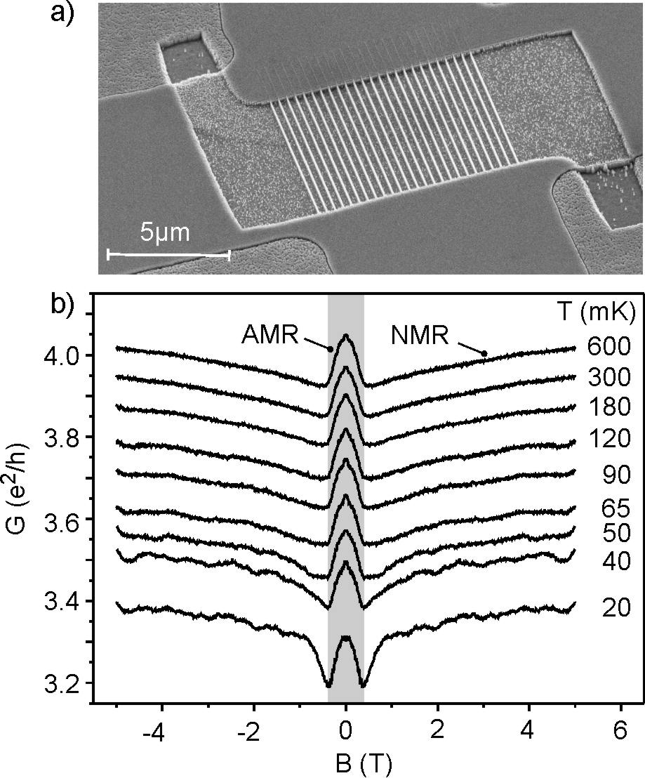
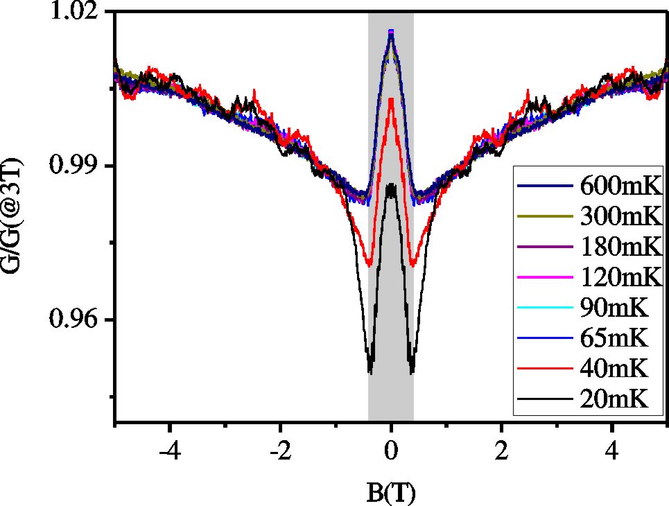
The two partial waves on time-reversed closed paths experience a spin rotation in opposite direction causing (partially) destructive interference [19]. So, SO interaction leads to reduced backscattering and reverses the sign of the WL, hence called weak antilocalization (WAL). A typical signature of WAL is a double dip in the magnetoconductance trace [19]. As a sufficient strong magnetic field removes time reversal symmetry, the question arises, whether weak localization can be observed at all in a ferromagnet. In conventional ferromagnets several experimental works explored this problem [39, 40, 41, 42], but a direct signature of weak localization was not found. The ferromagnetic semiconductor (Ga,Mn)As sheds new light to this question, as the internal magnetic field in ferromagnetic semiconductors is quite weak compared to conventional ferromagnets. To search for weak localization in the ferromagnetic semiconductor (Ga,Mn)As we fabricated arrays of wires connected in parallel (see table 1 sample a1-a2) and measured their resistance in a perpendicular applied magnetic field. By measuring an array of geometrically identical wires universal conductance fluctuations get suppressed by ensemble averaging. Also here the conductance was obtained by inverting the resistance, . In figure 8a an electron micrograph of sample a1 containing 25 nanowires in parallel is shown. The magnetoconductance [43] of sample a1 is shown in figure 8b for temperatures ranging from 600 mK down to 20 mK. We first start with the description of the dominant features observed in experiment. The conductance maximum around zero field is due to the so called anisotropic magneto resistance (marked AMR and grey shaded in figure 8b). Without applied magnetic field the magnetization of the (Ga,Mn)As wires lies in-plane. For such in-plane magnetization the conductance is higher than for an out-of-plane oriented magnetization [13]. Hence in the low- region the magnetization is rotated from in-plane to out-of-plane and causes the negative magnetoconductance. This magnetic field region is highlighted by grey-shading. At higher fields the positive slope of (marked NMR in figure 8b) is ascribed to an increase of magnetic order [44], or to 3D weak localization [45]. At temperatures above 65 mK the different traces are shifted without a noticeable change of their shape and the AMR height scales linearly with the background conductance. This is shown in Fig. 9, where the different traces are normalized to their (3T) value.
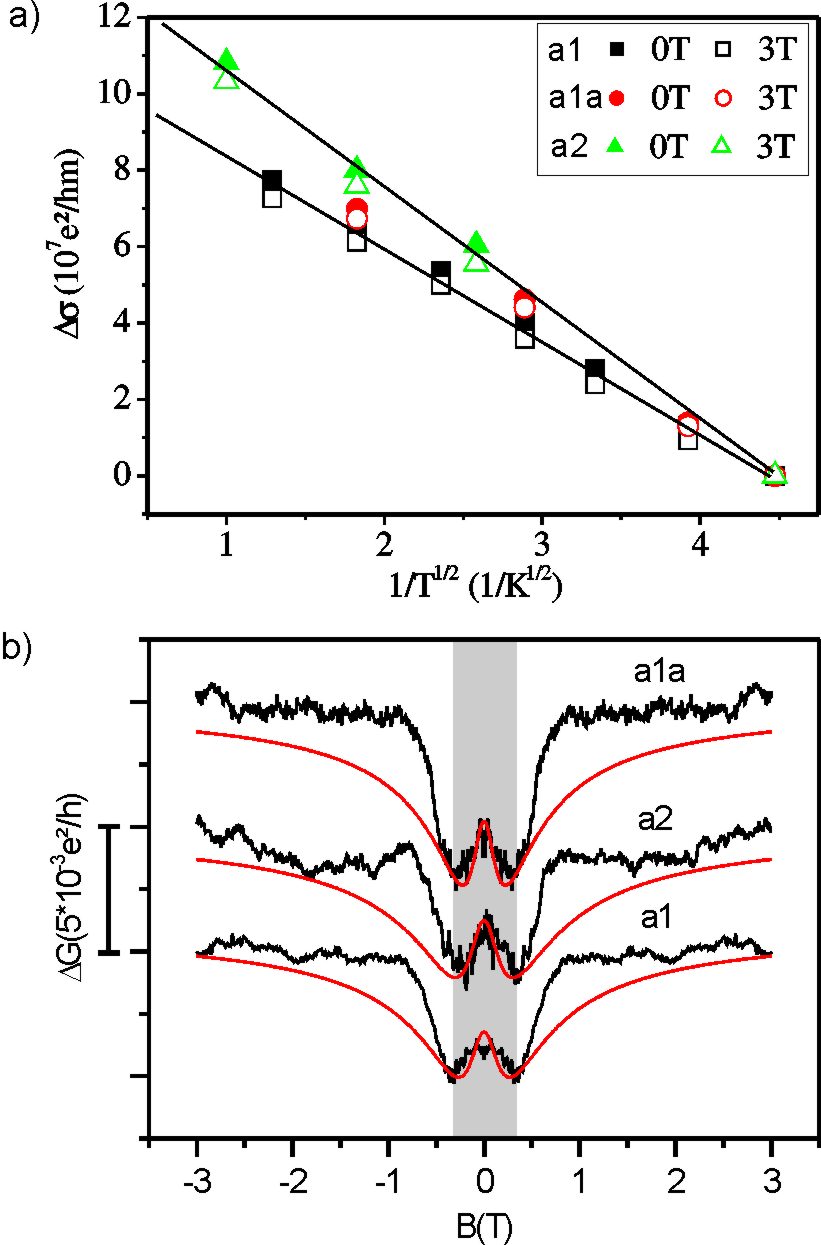
For temperatures between 65 mK and 600 mK all traces lie on top of each other. This means that the conductivity at different temperatures differs only by a constant factor , i.e., . The decreasing conductance with decreasing temperature displayed in figure 8b is due to electron-electron interaction (EEI). In contrast to the one-electron interference of scattered waves which causes weak localization, EEI results from interference of electron-electron interaction amplitudes corresponding to successive electron-electron scattering events in disordered systems [46, 47]. In contrast to WL, EEI is independent of magnetic field. In one dimensional samples the conductance decrease due to EEI follows a dependency [46]. This dependency is shown for the three investigated wire arrays in figure 10a. For all three wire samples the conductivity decrease follows such a dependency. The effect of electron-electron interactions in 1D and 2D (Ga,Mn)As is discussed in more detail in Ref. [48]. Here we only note that EEI is responsible for the shift of the traces at different temperatures in figure 8b. At mK two down cusps start to appear in the magnetoconductance of sample a1 in figure 8b at approx 400 mT and become a prominent feature at 20 mK. This is also seen in Fig. 9, were the different are normalized to their T) value. While the high temperature traces lie all on top of each other, the low temperature traces show two downward cusps with a size becoming comparable to the AMR at 20 mK. To separate this novel effect from the other transport contributions we have to subtract the high temperature background containing AMR and NMR. Here, we assume that the background scales like at temperatures above 50 mK, i.e. that . Here we have chosen the conductance at 120 mK as reference conductance to account for the background. The factor takes the linear scaling of AMR and NMR with the conductance value into account. We notice that the choice of the reference trace, we subtract, has an indiscernible influence on the result as the high temperature traces lie all on top of each other when normalized. The resulting traces which we ascribe to the weak localization correction are shown in figure 10b for all 3 samples (a1 - a2 in table 1). All three traces in figure 10b display a local conductance maxima at = 0 and two conductance minima at mT. Such shape is typical for the effect of weak antilocalization in systems with spin-orbit interaction. To extract the characteristic lengths from the data we utilize existing theory. The correction due to WAL in a quasi 1D system is given by [49, 32]:
| (3) |
where is the spin degeneracy, is the spin orbit scattering length describing the strength of spin orbit interaction, and is the magnetic length. Equation (3) is valid as long as the quasi 1D assumption is justified: .
With the value extracted from previous experiments, discussed above, this is justified for mK and mT. As the valence band in ferromagnetic (Ga,Mn)As is spin split, the holes are highly (but not fully) spin polarized [50]. To account for spin polarization, we approximated either by 1 (fully spin polarized) or by 2 (spin degenerate) as adjustable parameter. As fits with can’t describe the experimental results we resort to below (The fit with for sample a1 is shown in Ref. [51]). Corresponding fits are presented in figure 10b as red lines. The fit parameters are nm and nm for sample a1, nm and nm for sample a1a, and nm and nm for sample a2. While the fits are in good agreement with experiment for mT they are less satisfying at higher fields. The WL or WAL correction is, as a function of increasing , more abruptly suppressed than expected from theory. There is a striking correlation with the magnetic field dependence of the AMR effect. The magnetic field region where the AMR occurs is highlighted by gray shading in figures 8b, 9 and 10b. Within this -field range, the magnetization is rotated from in-plane to out-of-plane. Once the magnetization is out-of-plane, the WL correction drops quickly. At the same magnetic field, the magnetic length matches wire width and thickness, . Hence, the discrepancy between fit and experiment might be associated with dimensional crossover (1D to 3D), if exceeds 400 mT and equation (3) might be inapplicable. We further note that neither the field dependent change of the magnetization direction nor the 3/2-spin of the involved hole states was taken into account as the theory was developed for spin 1/2 electrons in disordered metals. Especially, the latter could add a number of additional interference diagrams not yet treated theoretically.
While weak antilocalization has already been observed in nonmagnetic p-type (Al,Ga)As/GaAs quantum wells [52], the observation in a ferromagnet came as a surprise. A recent theory suggests that the process leading to weak antilocalization is totally suppressed in a ferromagnet due to the spin-splitting which excludes a contribution of the so called singlet Cooperon diagram, responsible for WAL [53]. This theory was calculated for a quite strong ferromagnet with relatively high mean free path. This is not the case for (Ga,Mn)As and the observation of WAL in (Ga,Mn)As is not excluded by this theory [54, 55].
Also in this experiment we measured the magnetoconductance of one sample before and after annealing (Sample a1 and a1a) and compared the resulting phase coherence length. Here, the change of the phase coherence length was 27 %. Again, this change can again be ascribed to a change of the diffusion constant, while the relevant dephasing time stayed nearly unchanged (see table 1). This underlines that the Mn interstitials do not cause dephasing.
With the knowledge of we now can give a more precise value of the dephasing length extracted from the UCF measurement discussed in section 3. The dephasing length is dependent on the fluctuation amplitude , the wire length and a prefactor by . To determine the prefactor knowledge of the ratio of is necessary [24]. For a ratio (taking a spin orbit scattering length of 100 nm and a dephasing length of 150 nm) we get a prefactor of [24]. As we also deal with relatively high magnetic field ( T…15 T) where no weak localization can be observed the prefactor is reduced by a factor of . This factor is due to the absence of the cooperon term at high [23]. Taking this into account we obtain a prefactor of . At 20 mK this leads to dephasing lengths for the samples w1, w2, w3, w4, w5, r1 and r1a ranging from 90 nm to 160 nm (see table 1). These values are in very good agreement with the ones extracted from the amplitude of the Aharonov-Bohm oscillations ( nm) and the ones obtained by fitting the weak localization correction ( nm to 190 nm).
6 Conclusion
We investigated phase coherent transport in the ferromagnetic semiconductor (Ga,Mn)As by measuring universal conductance fluctuations, Aharonov-Bohm oscillations and weak localization. All three methods reveal a phase breaking length of 90-190 nm at 20 mK. By investigating universal conductance fluctuations at different temperatures we found a temperature dependency of . As main source of dephasing electron-electron scattering or in our case hole-hole scattering was identified by investigating the temperature and excitation current dependency of the UCFs. This is consistent with the quite weak temperature dependency of . The Mn interstitials do not cause dephasing; low temperature annealing increases the dephasing length only due to an increase of the diffusion constant, while the corresponding dephasing time stays unchanged. The magnetotransport in arrays of wires is modified by weak localization at temperatures below 50 mK, showing that time reversed interference effects can be observed in a ferromagnet. The existence of weak antilocalization shows that spin-orbit interaction is affecting the transport in (Ga,Mn)As. The corresponding spin orbit scattering length is always shorter than and of order 100 nm.
References
References
- [1] H. Ohno, H. Munekata, T. Penney, S. von Molnár, and L. L. Chang, Phys. Rev. Lett. 68, 2664 (1992).
- [2] H. Ohno, A. Shen, F. Matsukura, A. Oiwa, A. Endo, S. Katsumoto, and Y. Iye, Appl. Phys. Lett. 69, 363 (1996).
- [3] H. Ohno, Science 281, 951 (1998).
- [4] H. Ohno, J. Magn. Magn. Mater. 200, 110 (1999).
- [5] H. Ohno and F. Matsukura, Solid State Commun. 117, 179 (2001).
- [6] T. Dietl, Semicond. Sci. Technol. 17, 377 (2002).
- [7] A. H. MacDonald, P. Schiffer, and N. Samarth, Nat. Mater. 4, 195 (2005).
- [8] H. Ohno, D. Chiba, F. Matsukura, T. Omiya, E. Abe, T. Dietl, Y. Ohno, and K. Ohtani, Nature (London) 408, 944 (2000).
- [9] A. Oiwa, S. Katsumoto, A. Endo, M. Hirasawa, Y. Iye, H. Ohno, F. Matsukura, A. Shen, and Y. Sugawara, Solid State Commun. 103, 209 (1997).
- [10] T. Dietl, A. Haury, and Y. M. d’Aubigné, Phys. Rev. B 55, R3347 (1997).
- [11] T. Dietl, H. Ohno, F. Matsukura, J. Cibert, and D. Ferrand, Science 287, 1019 (2000).
- [12] M. Sawicki, J. Magn. Magn. Mater. 300, 1 (2006) and references therein.
- [13] D. V. Baxter, D. Ruzmetov, J. Scherschligt, Y. Sasaki, X. Liu, J. K. Furdyna, and C. H. Mielke, Phys. Rev. B 65, 212407 (2002).
- [14] T. Jungwirth, Jairo Sinova, J. Masek, J. Kucera, and A. H. MacDonald, Rev. Mod. Phys. 78, 809 (2006).
- [15] T. Jungwirth, K. Y. Wang, J. Masek, K. W. Edmonds, J. König, J. Sinova, M. Polini, N. A. Goncharuk, A. H. MacDonald, M. Sawicki, A. W. Rushforth, R. P. Campion, L. X. Zhao, C. T. Foxon, and B. L. Gallagher, Phys. Rev. B 72, 165204 (2005).
- [16] K. W. Edmonds, P. Boguslawski, K. Y. Wang, R. P. Campion, S. N. Novikov, N. R. S. Farley, B. L. Gallagher, C. T. Foxon, M. Sawicki, T. Dietl, M. Buongiorno Nardelli, and J. Bernholc, Phys. Rev. Lett. 92, 037201 (2004).
- [17] K. Y. Wang, R. Campion, K. Edmonds, M. Sawicki, T. Dietl, C. Foxon, and B. Gallagher, AIP Conf. Proc. 772, 333 (2005).
- [18] A. M. Nazmul, T. Amemiya, Y. Shuto, S. Sugahara, and M. Tanaka, Phys. Rev. Lett. 95, 017201 (2005).
- [19] G. Bergmann, Phys. Rep. 107, 1 (1984).
- [20] M. Reinwald, U. Wurstbauer, M. Döppe, W. Kipferl, K. Wagenhuber, H.-P. Tranitz, D. Weiss and W. Wegscheider, J. Cryst. Growth 278, 690 (2005).
- [21] A. Hubert and R. Schäfer, Magnetic Domains, Springer (Berlin) (1998).
- [22] S. Washburn and R. A. Webb, Rep. Prog. Phys. 55, 1311 (1992).
- [23] P. A. Lee, A. D. Stone, and H. Fukuyama, Phys. Rev. B 35, 1039 (1987).
- [24] V. Chandrasekhar, P. Santhanam, and D. E. Prober, Phys. Rev. B 42, 6823 (1990).
- [25] K. Wagner, D. Neumaier, M. Reinwald, W. Wegscheider, and D. Weiss, Phys. Rev. Lett. 97, 056803 (2006).
- [26] L. Vila, R. Giraud, L. Thevenard, A. Lemaître, F. Pierre, J. Dufouleur, D. Mailly, B. Barbara, and G. Faini, Phys. Rev. Lett. 98, 027204 (2007).
- [27] A. Sergeev and V. Mitin, Europhys. Lett. 51, 641 (2000).
- [28] Y. Takane, J. Phys. Soc. Jpn. 72, 1155 (2003).
- [29] B. L. Altshuler, A. G. Aronov, and D. E. Khmelnitsky, J. Phys. C 15, 7367 (1982).
- [30] P. Dai, Y. Zhang, and M. P. Sarachik, Phys. Rev. B 46, 6724 (1992).
- [31] F. C. Wellstood, C. Urbina, and J. Clarke, Phys. Rev. B 49, 5942 (1994).
- [32] F. Pierre, A. B. Gougam, A. Anthore, H. Pothier, D. Esteve, and Norman O. Birge, Phys. Rev. B 68, 085413 (2003).
- [33] P. Mohanty and R. A. Webb, Phys. Rev. Lett.91, 066604 (2003).
- [34] S. Washburn and R. Webb, Adv. Phys. 35, 375 (1986).
- [35] A. Fuhrer, S. Lüscher, T. Ihn, T. Heinzel, K. Ensslin, W. Wegscheider and M. Bichler, Nature 413, 822 (2001).
- [36] B. Garbić, Renaud Leturcq, Thomas Ihn, Klaus Ensslin, Dirk Reuter, and Andreas D. Wieck, Phys. Rev. Lett. 99, 176803 (2007).
- [37] S. Kasai, E. Saitoh, and H. Miyajima, Appl. Phys. Lett. 81, 316 (2002).
- [38] The conductance shown in figure 7b and 7c is the conductance of the ring and the leads up to the voltage probe. Equation (2) describes only the conductance oscillation of the ring only. This issue has to be taken into account when calculating the phase coherence length.
- [39] M. Brands, A. Carl, O. Posth, and G. Dumpich, Phys. Rev. B 72, 085457 (2005).
- [40] M. Brands, C. Hassel, A. Carl, and G. Dumpich, Phys. Rev. B 74, 033406 (2006).
- [41] T. Ono, Y. Ooka, S. Kasai, H. Miyajima, K. Mibu and T. Shinjo, J. Magn. Magn. Mater. 226, 1831 (2001).
- [42] M. Aprili, J. Lesueur, L. Dumoulin and P. Nédellec, Solid State Commun. 102, 41 (1997).
- [43] In sample a1 and a1a the two voltage leads were fabricated on opposite sites. So, also the Hall conductance was measured. To remove the Hall conductance from the data only the symmetric part of the trace was taken. As this leads to the same result than seen on sample a2, where the voltage leads are on the same side, physics is not changed by this procedure.
- [44] E. L. Nagaev, Phys. Rev. B 58, 816 (1998).
- [45] F. Matsukura, M. Sawicki, T. Dietl, D. Chiba, and H. Ohno, Physica E 21, 1032 (2004).
- [46] P. A. Lee and T. V. Ramakrishnan , Rev. Mod. Phys. 57, 287 (1985).
- [47] T. Dietl, arXiv:0712.1293v2.
- [48] D. Neumaier, M. Schlapps, U. Wurstbauer, J. Sadowski, M. Reinwald, W. Wegscheider, and D. Weiss, arXiv:0711.3278v2.
- [49] B. L. Altshuler and A. G. Aronov, JETP Lett 33, 499 (1981).
- [50] J. G. Braden, J. S. Parker, P. Xiong, S. H. Chun, and N. Samarth, Phys. Rev. Lett. 91, 056602 (2003).
- [51] D. Neumaier, K. Wagner, S. Geißler, U. Wurstbauer, J. Sadowski, W. Wegscheider, and D. Weiss, Phys. Rev. Lett. 99, 116803 (2007).
- [52] S. Pedersen, C. B. Sørensen, A. Kristensen, P. E. Lindelof, L. E. Golub, and N. S. Averkiev, Phys. Rev. B 60, 4880 (1999).
- [53] V. K. Dugaev, P. Bruno, and J. Barnaś, Phys. Rev. B 64, 144423 (2001).
- [54] V. K. Dugaev, private communication (2007).
- [55] S. Sil, P. Entel, G. Dumpich, and M. Brands, Phys. Rev. B 72, 174401 (2005).
