Measurement of the Optical Absorption Spectra of Epitaxial Graphene from Terahertz to Visible
Abstract
We present experimental results on the optical absorption spectra of epitaxial graphene from the visible to the terahertz (THz) frequency range. In the THz range, the absorption is dominated by intraband processes with a frequency dependence similar to the Drude model. In the near IR range, the absorption is due to interband processes and the measured optical conductivity is close to the theoretical value of . We extract values for the carrier densities, the number of carbon atom layers, and the intraband scattering times from the measurements.
Graphene is a single atomic layer of carbon atoms forming a honeycomb crystal lattice dressel ; nov0 . The unusual electronic and optical properties of graphene have generated interest in both experimental and theoretical arenas nov0 ; nov1 ; NovoselovGeimFirst ; zhang ; heer . The high mobility of electrons in graphene has prompted a large number of investigations into graphene based high speed electronic devices, such as field-effect transistors and pn-junction diodes, photonic devices, such as terahertz oscillators, and also low noise electronic and optical sensors NovoselovGeimFirst ; lundstrom ; marcus ; gong ; rana ; chemicalsensor . For many of these applications, knowledge of the optical properties of graphene is critical.
Graphene layers can be obtained via micromechanical cleaving (exfoliation) of bulk graphite followed by careful selection of monolayers by using optical, atomic force, or scanning electron microscopes nov1 . Although this technique results in relatively high quality films, it might not be suitable for large scale production. Recently, epitaxial growth of graphene by thermal decomposition of SiC surface at high temperatures has been demonstrated heer ; grapheneonSiC1 . This technique can provide anywhere from a few monolayers of graphene to several () layers on the surface of a SiC wafer. Graphene layers grown by this technique have demonstrated low temperature carrier mobilities in the few tens of thousand cm2/V-s range heer . In addition, the electronic as well phononic properties of epitaxially grown graphene multilayers have been found to be different from those of bulk graphite and similar to those of a graphene monolayer raman ; stacking1 ; stacking2 ; stacking3 . This observed difference in the properties of epitaxial graphene and bulk graphite has been attributed to a different stacking scheme for carbon atom layers in epitaxial graphene compared to that in bulk graphite in which the layers are stacked according to the Bernal scheme stacking1 ; stacking2 ; stacking3 . Although the band energy dispersion in carbon atom multilayers can exhibit massless Dirac Fermion like behavior at small energies for various different stacking schemes and interlayer couplings, the band energy dispersions at large energies can be significantly different stacking2 ; stacking3 . The exact structure of epitaxial graphene and the nature of interlayer couplings remain active areas of investigation. Measurement of the optical absorption spectra over a wide frequency range can provide useful information about the structure of epitaxial graphene.
In the visible to the mid-IR wavelength range ( m), the optical absorption spectra of exfoliated graphene monolayers has been reported recently stormer ; geimopt ; heinz . In this paper, we report results from measurements of the optical absorption spectra of epitaxial graphene from the visible to the terahertz frequency range for the first time and compare the results with the theoretical predictions for graphene. In graphene, the valence and conduction bands resulting from the mixing of the -orbitals are degenerate at the K (K’) points of the Brillouin zone. Near these points, the tight-binding Hamiltonian in the nearest-neighbor approximation , using the basis consisting of orbitals centered on the and atoms, can be linearized and written as dressel ,
| (1) |
where m/s is the Fermi velocity. This Hamiltonian results in the energy dispersion relation for the conduction and valence bands given by, . The bandgap is equal to and could acquire a non-zero value as a result of any interaction that breaks the symmetry between the and atoms in the unit cell of graphene. Optical absorption in graphene is described by the optical conductivity . It can be written as the sum of the interband conductivity and the intraband conductivity , both of which can be found using the Hamiltonian above and are given below rana ; sharapov .
| (2) | |||||
| (3) | |||||
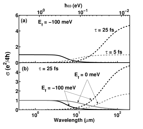
Here, is the Fermi distribution function with Fermi enery , describes the broadening of the interband transitions, and is the momentum relaxation time due to carrier intraband scattering. The frequency dependencies of the real parts of and are depicted in Fig.1, assuming , meV and T=300K. Fig.1(a) shows the conductivities for meV and two different values of the scattering time : 25 fs and 5 fs. Fig.1(b) shows the conductivities for equal to 25 fs and two different values of the fermi energy : 0 meV and -100 meV. At large frequencies, the real part of has a constant value equal to . At small frequencies, the real part of approaches zero because interband optical transitions are blocked due to the presence of electrons and holes near the band edges. The plasmon dispersion and the free-carrier absorption in graphene are described by . Its frequency dependence is similar to that of a Drude model, as it is evident from the pre-factor in Eq.(3). The real part of approaches zero for large frequencies at which carriers are unable to respond. At small frequencies, the real part of approaches the DC conductivity of graphene. Fig.1 (b) shows that the spectral shape of at small frequencies is strongly influenced by the intraband carrier scattering time . The total conductivity has a minimum in the frequency range where both and are small.

The epitaxial graphene samples used in this work were grown on the carbon face of semi-insulating 6H-SiC wafers using the techniques that have been reported in detail previously grapheneonSiC1 . The samples were grown at temperatures of - and pressures of torr. The number of carbon atom layers in each sample were estimated through X-ray photoelectron spectroscopy (XPS) using the Thickogram method thicko . Raman spectroscopy (using excitation wavelength of 488 nm) of the samples showed a single-resonant G peak close to 1580 cm-1, a double-resonant D’ peak close to 2700 cm-1, and also a relatively low intensity double-resonant D peak near 1350 cm-1 raman ; raman1 . The D peak is not allowed in perfect graphene layers since it requires an elastic scattering process, which is made possible by disorder, to satisfy momentum conservation raman . The presence of the D peak, therefore, indicates the presence of disorder in the samples. The ratio of the intensities of the G and D peaks () has been shown to be proportional to the crystal coherence length ramandis . The ratio for samples A, B and C were 13, 17 and2 respectively, indicating that sample C has a much larger level of disorder compared to the other two samples. Ultrafast carrier dynamics in samples A and B have been studied in a previous work dawlaty . Sample C reported in this paper is not the same as the one reported in our earlier studydawlaty .
Three different instruments were used to measure the optical transmission through the graphene samples. In the visible to the near-IR wavelength range (0.4-0.9 m) a grating spectrometer was used. In the near-IR to the mid-IR range (1.4-25 m) a mid-IR Fourier Transform IR (FTIR) spectrometer was used. And in the mid-IR to the far-IR (terahertz) wavelength range (15-200 m) a far-IR FTIR spectrometer was used. The measured transmission spectrum for each sample was normalized to the transmission spectrum of a reference SiC wafer. A small (few mm size) aperture was used to ensure transmission through equal areas of the sample and the reference and also to avoid corruption of data when changing instruments due to possible non-uniformities in the sample. The SiC substrate transmits very little in the 6-14 m wavelength range due to multi-phonon absorption sicbands . As a result, the measured transmission spectra had poor signal-to-noise ratios in this wavelength range. The fringes in the transmission spectra arising from multiple reflections within the SiC substrate were numerically filtered out after normalizing with respect to the transmission spectrum of the reference SiC wafer.


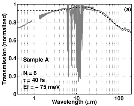
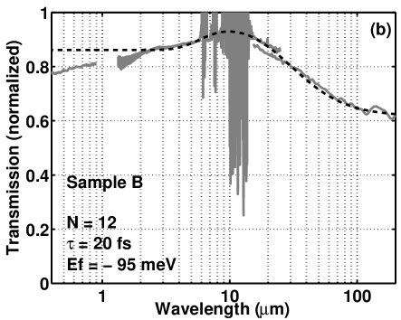
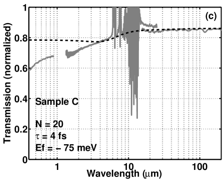
Fig.2 shows the normalized transmission spectra through the epitaxial graphene samples A, B and C. The optical absorption in the graphene layers depends sensitively on the substrate index of refraction. Matching the optical boundary conditions at the air/graphene/SiC interfaces, the optical transmission through graphene layers on a SiC wafer (normalized to the transmission through a plain SiC wafer) can be written in terms of the complex optical conductivity as,
| (4) |
where 2.55 is the refractive index of SiC. For , is related to only the real part of the optical conductivity and can therefore be used to measure the absorption spectra of graphene. We have used Eqs.(2)-(4) to model the measured transmission data using , , as the fitting parameters. The parameters and were assumed to be 10 meV and 0 meV respectively. Changing the values of and by small amounts (much less than ) had little effect on the final results. The dashed black lines in Fig.2 are the theoretical fits to the experimental data (solid gray lines). The values of the fitting parameters are shown in the insets. A 5-10 variation in any one of the parameters, , ,and , produces a noticeable degradation in the quality of the theoretical fit to the data.
The number of graphene layers obtained this way agrees well with the value obtained through XPS. For example, the XPS method gave values of equal to 6 and 11 for samples A and B respectively. The extracted values of the Fermi energy correspond to average carrier densities of cm-2 and cm-2 per layer for samples A and B, respectively. Due to the electron-hole symmetry of the graphene bandstructure near the band edge, both negative and positive signs of the Fermi energy will fit the experimental data equally well. Also note that the experiments only give information on the total conductivity of all the layers, and therefore the extracted value of the Fermi energy should be taken as an average value for all the layers. Recent work on epitaxial graphene suggests that a concentration of carriers larger than the intrinsic value is expected only in the first few carbon atom layers near the SiC interface. Assuming that only the first two layers have non-zero Fermi levels and the remaining layers are intrinsic, values of the Fermi level equal to -150 meV and -290 meV for the first two layers of samples A and B, respectively, provide good fits to the measured data. As mentioned earlier, Sample C is significantly more disordered than Samples A and B. The transmission spectra of Sample C shows a distinctly different shape in the THz region (Fig.2c), which can be fitted well with a very short carrier scattering time of 4 fs.
It has been recently pointed out that the first few graphene layers in epitaxially grown graphene could acquire a bandgap as a result of interaction with the atoms in the SiC substrate heer2 . Although a value of equal to zero was found to fit our measured data well, a value of much smaller than would be difficult to detect in our measurements. A non-zero value of the bandgap in the mid-IR to far-IR range, where the intraband contribution to the conductivity dominates, would have little effect on the transmission spectra. If the value of the bandgap is in the near-IR to the mid-IR range, its effects at room temperature would be hard to distinguish from the reduction in the interband conductivity at small frequencies due to band filling effects (see Fig.1(b)). Also, in multilayer graphene structures the optical response is dominated by the large number of layers that are not close to the substrate and do not have a bandgap.
The short wavelength end of the measured transmission spectra in Fig.2 deviates from the theoretical predictions for wavelengths shorter than m. The deviation is minimum for sample B and corresponds to 50 more absorption at 0.4 m compared to the theory. The reasons for this deviation are not clear. Two factors could be responsible for this behavior: (i) the band energy dispersion and interband optical matrix elements at large energies are different from those obtained from the Hamiltonian given in Eq.(2), and (ii) increased light scattering may be expected from the sample at shorter wavelengths as the wavelength approaches the crystal coherence length (50-100 nm). Using a full-band tight-binding model for a graphene monolayer that includes second and third neighbor interactions tbaccurate , and using the method for calculating the interband optical matrix elements described by Johnson et. al. dressel2 , we obtain values of the optical interband conductivity that deviate from only for wavelengths shorter than 1.5 m and are only larger than at wavelengths close to 0.4 m. Therefore, effects related to trigonal warping and deviation of bands from linearity cannot be completely responsible for the observed discrepancy. The band energy dispersion in epitaxial graphene at large energies could also be affected by the nature of the interlayer couplings. Note that the deviation of the measured transmission spectra from the theory is not the same for the three samples indicating that disorder might also have a role to play. More work is needed to investigate the nature of this discrepancy.
In conclusion, we have measured the optical absorption spectra of epitaxial graphene from the terahertz to the visible frequencies. The experimental results have been shown to be in agreement with the theory except at short wavelengths. Our results confirm the Drude-like frequency dependence of the intraband conductivity of graphene in the THz frequency range. The results presented here indicate that absorption spectroscopy can be used as a noninvasive technique to characterize graphene films and find the values of parameters, such as the Fermi energy and the carrier density, carrier intraband scattering time, and the number of graphene layers. The authors acknowledge support from the National Science Foundation, the Air Force office of Scientific research contract No. FA9550-07-1-0332 (contract monitor Dr. Donald Silversmith) and Cornell Material Science and Engineering Center (CCMR) program of the National Science Foundation (cooperative agreement 0520404).
References
- (1) R. Saito, G. Dresselhaus, M. S. Dresselhaus, Physical Properties of Carbon Nanotubes, Imperial College Press, London, UK (1999).
- (2) A. H. Castro Neto, F. Guinea, N. M. R. Peres, K. S. Novoselov, A. K. Geim, Submitted to Rev. Mod. Phys. (2007). Also available at cond-mat/0709.1163 (2007).
- (3) K. S. Novoselov, A. K. Geim, S. V. Morozov, D. Jiang, M. I. Katsnelson, I. V. Grigorieva, S. V. Dubonos, A. A. Firsov, Nature, 438, 197 (2005).
- (4) K.S. Novoselov, A.K. Geim, S.V. Morozov, D. Jiang, Y. Zhang, S. V. Dubonos, I.V. Grigorieva, A.A. Firsov, Science, 306, 666 - 669 (2004).
- (5) Y. Zhang, Y. Tan, H. L. Stormer, P. Kim, Nature, 438, 201 (2005).
- (6) C. Berger, Z. Song, X. Li, X. Wu, N. Brown, C. Naud, D. Mayou, T. Li, J. Hass, A. N. Marchenkov, E. H. Conrad, P. N. First, W. A. de Heer, Science, 312, 1191 (2006).
- (7) G. Liang, N. Neophytou, D. E. Nikonov, M. S. Lundstrom, IEEE Trans. Elec. Dev., 54, 657 (2007).
- (8) J. R. Williams, L. DiCarlo, C. M. Marcus, Science, 317, 638 (2007).
- (9) G. Gu, S. Nie, R. M. Feenstra, R. P. Devaty, W. J. Choyke, W. K. Chan, M. G. Kane, Appl. Phys. Lett., 90, 253507 (2007).
- (10) F. Rana, IEEE Trans. Nanotechnology, 7, 91-99 (2008).
- (11) F. Schedin, A.K. Geim, S.V. Morozov, E.W. Hill, P. Blake, M.I. Katsnelson, K.S. Novoselov , Nature Materials 6, 652 (2007).
- (12) C. Berger, Z. Song, T. Li, X. Li, A. Y. Ogbazghi, R. Feng, Z. Dai, A.N. Marchenkov, E.H. Conrad, P.N. First, W.A. de Heer , J. Phys. Chem. B 108, 19912 (2004).
- (13) C. Faugeras, A. Nerriere, M. Potemski, A. Mahmood, E. Dujardin, C. Berger, W. A. de Heer, cond-mat/0709.2538 (2007).
- (14) J. Hass, F. Varchon, J. E. Millan-Otoya, M. Sprinkle, W. A. de Heer, C. Berger, P. N. First, L. Magaud, E. H. Conrad, cond-mat/0706.2134 (2007).
- (15) S. Latil, V. Meunier, L. Henrard1, Phys. Rev. B, 76, 201402(R) (2007).
- (16) J. M. B. Lopes dos Santos, N. M. R. Peres, A. H. Castro Neto, Phys. Rev. Lett., 99, 256802 (2007).
- (17) Z. Q. Li, E. A. Henriksen, Z. Jiang, Z. Hao, M. C. Martin, P. Kim, H. L. Stormer, D. N. Basov, Nature Physics, 4, 532 (2008).
- (18) R. R. Nair, P. Blake, A. N. Grigorenko, K. S. Novoselov, T. J. Booth, T. Stauber, N. M. R. Peres, A. K. Geim, Science, 320, 1308 (2008).
- (19) K. F. Mak , M. Sfeir , Y. Wu , C. H. Lui , J. Maultzsch , S. Rosenblatt , M. Hybertsen , T. Heinz, Bul. of Am. Phys. Soc. 53, L29.3 (2008).
- (20) V. P. Gusynin, S. G. Sharapov, J. P. Carbotte2, Phys. Rev. Lett., 96, 256802 (2006). V. P. Gusynin, S. G. Sharapov, J.P. Carbotte, J. Phys. Cond. Matt., 19 026222 (2007).
- (21) A. C. Ferrari, J. C. Meyer, V. Scardaci, C. Casiraghi, M. Lazzeri, F. Mauri, S. Piscanec, D. Jiang, K. S. Novoselov, S. Roth, A. K. Geim, Phys. Rev. Letts., 97, 187401 (2006).
- (22) J. M. Dawlaty, S. Shivaraman, M. Chandrashekhar, F. Rana, M. G. Spencer, Appl. Phys. Lett., 92 42116 (2008)
- (23) P. J Cumpson, Surface and Interface Analysis, 29, 403 (2000).
- (24) A. S. Bakin, S. I. Dorozhkin, A. S. Zubrilov, Proc. 4th Int. High Temp. Elec. Conf. (HITEC), 253-256 (1998).
- (25) A. C. Ferrari, J. Robertson, Phys. Rev. B, 61, 14095 (2000).
- (26) S. Reich, J. Maultzsch, C. Thomsen, P. Ordejon, Phys. Rev. B., 66, 035412 (2002).
- (27) L. G. Johnson, G. Dresselhaus, Phys. Rev. B, 7, 2275 (1973).
- (28) S.Y. Zhou, G. H. Gweon, A. V. Fedorov, P. N. First, W. A. de Heer, D. H. Lee, F. Guinea, A. H. Castro Neto, A. Lanzara, Nature Materials, 6, 770 (2007).