Trapping molecules on a chip in traveling potential wells
Abstract
A microstructured array of over electrodes on a substrate has been configured to generate an array of local minima of electric field strength with a periodicity of m about m above the substrate. By applying sinusoidally varying potentials to the electrodes, these minima can be made to move smoothly along the array. Polar molecules in low field seeking quantum states can be trapped in these traveling potential wells. This is experimentally demonstrated by transporting metastable CO molecules in mK deep wells that move at constant velocities above the substrate.
pacs:
37.10.Mn, 37.10.Pq, 37.20.+j, 33.57.+cThe manipulation of ultracold atoms above a microchip using magnetic fields is currently a very active area of research. Although initially motivated by the strong confinement that results from miniaturization of guides and traps, chip technology also enables multiple tools and devices to be integrated into a single compact structure. Today, atom chips are therefore discussed in a far more general context and are, for instance, used for matter-wave interferometry and precision force sensing Fortagh-RMP-2007 . Via miniaturization, strong electric field gradients can be produced as well. This has been used to push atoms along a magnetic guide on a chip Kruger-PRL-2003 and to demonstrate ac electric trapping of atoms in a microscopic volume Kishimoto-PRL-2006 . The strong electric field gradients are also ideal for the precise manipulation of polar molecules on a chip. Such precision is required, for instance, for proposed schemes of quantum computation that use polar molecules as qubits DeMille-PRL-2002 ; Andre-NP-2006 .
Compared to atoms, molecules are more difficult to load and detect on a chip. The methods to produce the required dense samples of cold molecules are less matured. As molecules in general lack a closed two-level system, efficient detection using absorption or laser induced fluorescence is not possible. These difficulties have hindered experiments with molecules on chips, and thus far, only reflection of a slow beam of ammonia from a microstructured electrostatic mirror has been demonstrated Schulz-PRL-2004 .
In this Letter, we present the loading of polar molecules from a supersonic beam into traveling potential wells on a chip. Metastable CO molecules are captured in approximately mK deep wells and transported at velocities around m/s along the full cm length of a chip, and they are detected after leaving it. The operation principle of this “supersonic electric conveyor belt” on a chip is detailed, and its potential as decelerator is considered.
To explain the operation principle of the electric conveyor belt, we start by discussing the electric field distribution that can be generated above an array of equidistant, parallel electrodes. The width of the electrodes is taken to be m and the center-to-center distance between adjacent electrodes is m, the parameters used in the experiments described later. In Figs. 1(a)-1(c) contour lines of equal electric field strength are shown in the plane, in kV/cm intervals. The axis is perpendicular to the substrate, whereas the axis is along the substrate, perpendicular to the electrodes, which are indicated by horizontal black bars. The potentials applied to the electrodes are indicated directly above them (in volts). Calculations are performed for the two-dimensional case; i.e., the extension of the electrodes along the axis is taken to be infinite. Since the actual length of the electrodes used in the experiments is mm (), this approximation is justified. The strength of the electric field generated above the electrode array generally falls off rapidly with increasing height above the substrate. At specific locations above the substrate, however, local minima of the electric field are created. This is similar to the minima in magnetic field that can be created above an arrangement of four current carrying wires Dekker-PRL-2000 , and can be most easily understood when inspecting the electrode arrangement near the center of Fig. 1(a). With the potentials applied as shown, the electrodes at and m create an electric field that is parallel to the axis, in the direction of negative values, for any point along the vertical line at m. The electrodes at and m create an electric field that is pointing in the opposite direction for any point along this line. For short distances above the substrate, the field due to the two nearest electrodes dominates, whereas for distances further away, the field due to the next nearest electrodes is most important. It is clear, therefore, that at some point above the substrate, at a typical height on the order of , a zero of the electric field strength will be generated on the m axis. In this particular case, this minimum occurs at a height of m above the substrate.
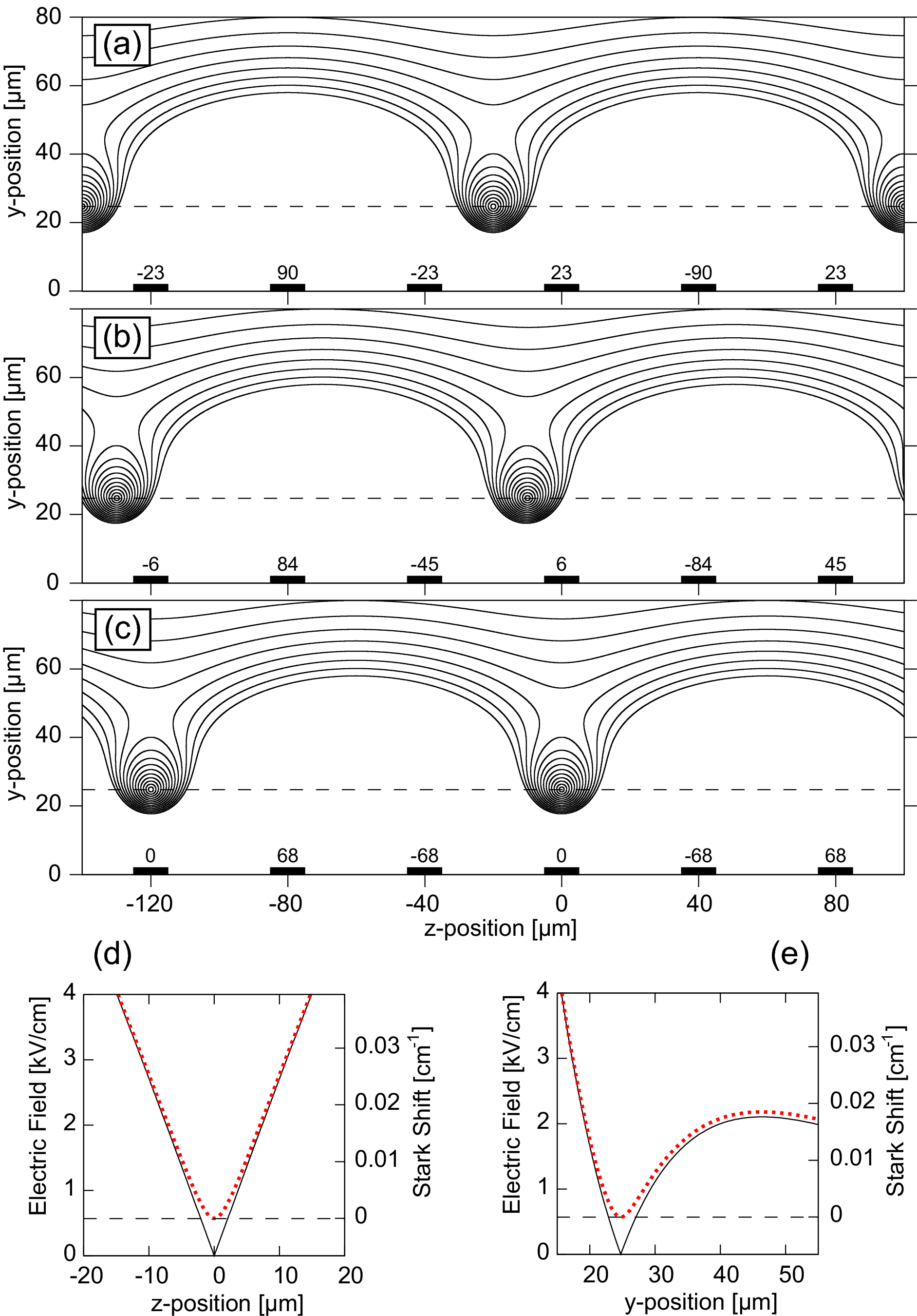
Rather than using static voltages, the potentials applied to all the electrodes are sinusoidally varying in time with an angular frequency , which is in the MHz range for our experiments. In each of the panels (a)-(c) the situation is shown at a given time ()-(), respectively, with (-) = (-) = . The different panels therefore show the instantaneous voltages and the resulting electric field distributions at phases of the rf cycle that are separated by . The voltage applied to the electrode from the left in Fig. 1(a) is given by , with V and equal to , , and , for , , and , respectively. For the nd, th, and th electrodes in Fig. 1(a), these voltages are , with equal to , , and , respectively. In this way, the potential on any given electrode is always equal in magnitude but opposite in sign to the potential on the electrodes that are three positions further. The six electrodes shown in Fig. 1(a) then form one full period and create two minima of the electric field strength above the substrate that are separated by , or m. Figures 1(b) and 1(c) are contour plots taken and later in the rf cycles, respectively. It can be seen from these three contour plots that the minima have almost the exact same shape and are located at an almost constant height above the substrate in any phase of the rf cycle. The calculated maximum difference in height when the minima move from the position between two electrodes to a position centered above an electrode is less than m. As a function of time the minima therefore move smoothly along the substrate, with a velocity given by .
Figures 1(d) and 1(e) show one-dimensional cuts through the electric field minimum above the electrode centered at m in panel (c). Along the axis, the electric field strength increases linearly with distance from the center at , like in an ideal quadrupole electric trap. Along the axis, the electric field strength has the same quadrupole behavior close to the minimum. For distances further away from the substrate, however, there is a slower increase followed by a saddle point of the electric field strength, limiting the overall depth of this electric trap to about kV/cm. The right vertical axes of Figs. 1(d) and 1(e) indicate the Stark shift that metastable CO () molecules in the low-field seeking component of the level experience in these electric fields Jongma-CPL-1997 . Because of the doubling, the Stark shift is quadratic for small values of the electric field. It is concluded that, above the array of electrodes, a traveling potential well with a depth of almost mK is created for these CO molecules. The shape of this potential well in the plane is approximately circular with a diameter of about m.
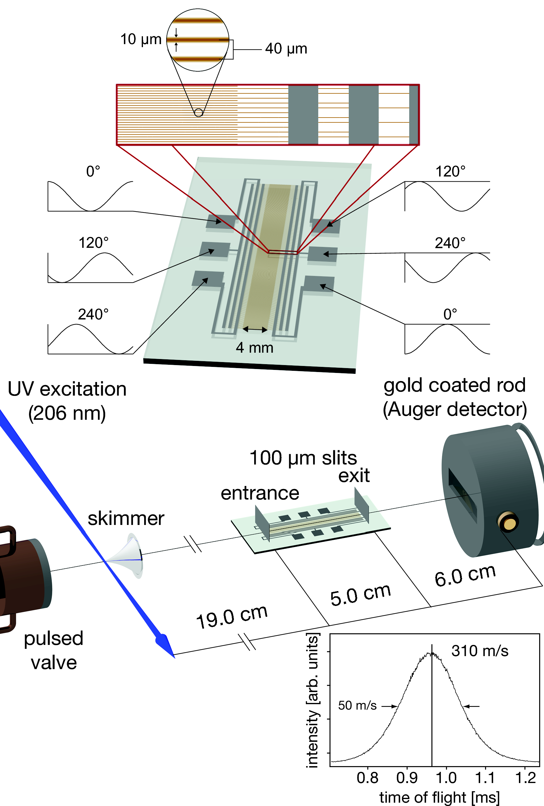
The actual implementation of the microstructured electrode array (micro resist technology GmbH) is shown in the upper part of Fig. 2. The m wide and approximately m thick gold electrodes are patterned on a glass substrate via lithographic etching. In total there are electrodes at a center-to-center distance of m, making for a total length of the structure of cm. As indicated, the “active region” in which all electrodes are equidistant extends over mm. The six different time-varying potentials that need to be applied to the electrode array are coupled in via the three macroscopic pads that are seen on either side of the structure. The three stripes that run along the long axis on each side of the active region and that supply the voltages to every sixth electrode, are actually at a slightly different height than the gold electrodes. A nm thin protecting and insulating intermediate layer prevents short circuits of the electrodes when they cross. This same layer, which has an electrical permittivity of , also covers the whole microstructured electrode array to reduce the risk of electrical breakdown. Its influence, as well as that of the glass substrate, has been taken into account in the calculated electric field distributions shown in Fig. 1.
A scheme of the experimental setup is shown in the central part of Fig. 2. A pulsed beam ( Hz) is formed by expanding a mixture of % CO in xenon into vacuum through a cooled solenoid valve. In the molecular beam, only the lowest rotational levels in the electronic and vibrational ground state of CO are occupied, and molecules in these levels interact only very weakly with external electric fields. Metastable CO () molecules, which experience a strong interaction with electric fields, are prepared in the low-field seeking component of the level via pulsed laser excitation on the transition of the band around nm. The radiative lifetime of this particular level is ms Gilijamse-JCP-2007 , sufficiently long for the experiments presented here. At the same time, this finite lifetime permits the recording of some laser induced phosphorescence signal just after the molecules have passed through the mm diameter skimmer into the second chamber; i.e., it allows for monitoring the beam intensity. About cm downstream from the laser excitation point, the molecules pass through an approximately m high entrance slit and then travel closely above the microstructured electrode array over the full cm length of the array. The molecular beam axis is thus parallel to the axis in Fig. 1, and it passes over the center of the mm electrodes. When no voltages are applied to the electrodes, a significant fraction of the metastable CO molecules that have passed through the entrance slit also passes through the about m high exit slit. Time-resolved detection of the metastable CO molecules, which have eV of electronic energy, is performed by recording the Auger electrons that are released from the central mm long area of a gold-coated rod when these molecules impinge on it. In the lower right corner of Fig. 2, the thus recorded arrival time distribution of the metastable CO molecules over the cm flight distance is shown. As the metastable CO molecules are produced by the weakly focused laser beam ( ns duration) in an about mm long region along the axis, the time on the horizontal axis can be directly related to the velocity. The peak velocity of the CO molecules is about m/s, and with a full-width-at-half-maximum (FWHM) of m/s the velocity spread is rather large.
When voltages are applied to the electrodes, the metastable CO molecules that pass through the entrance slit interact with the electric fields while flying closely above the substrate. Most of the molecules are in regions where the electric field gradient is predominantly perpendicular to the substrate, and these molecules are efficiently deflected away from the substrate Schulz-PRL-2004 . Consequently, these molecules no longer pass through the exit slit and will not be detected. Only the small fraction of the metastable CO molecules that happens to be near the minima of the electric field can be transported along the array to the other end. From purely geometrical arguments, this fraction is expected to be about . In addition, the molecules must have the right initial velocity to be captured in one of the traveling potential wells. At a given frequency , only an ensemble of molecules with a FWHM velocity spread of about m/s around the central velocity will be accepted.
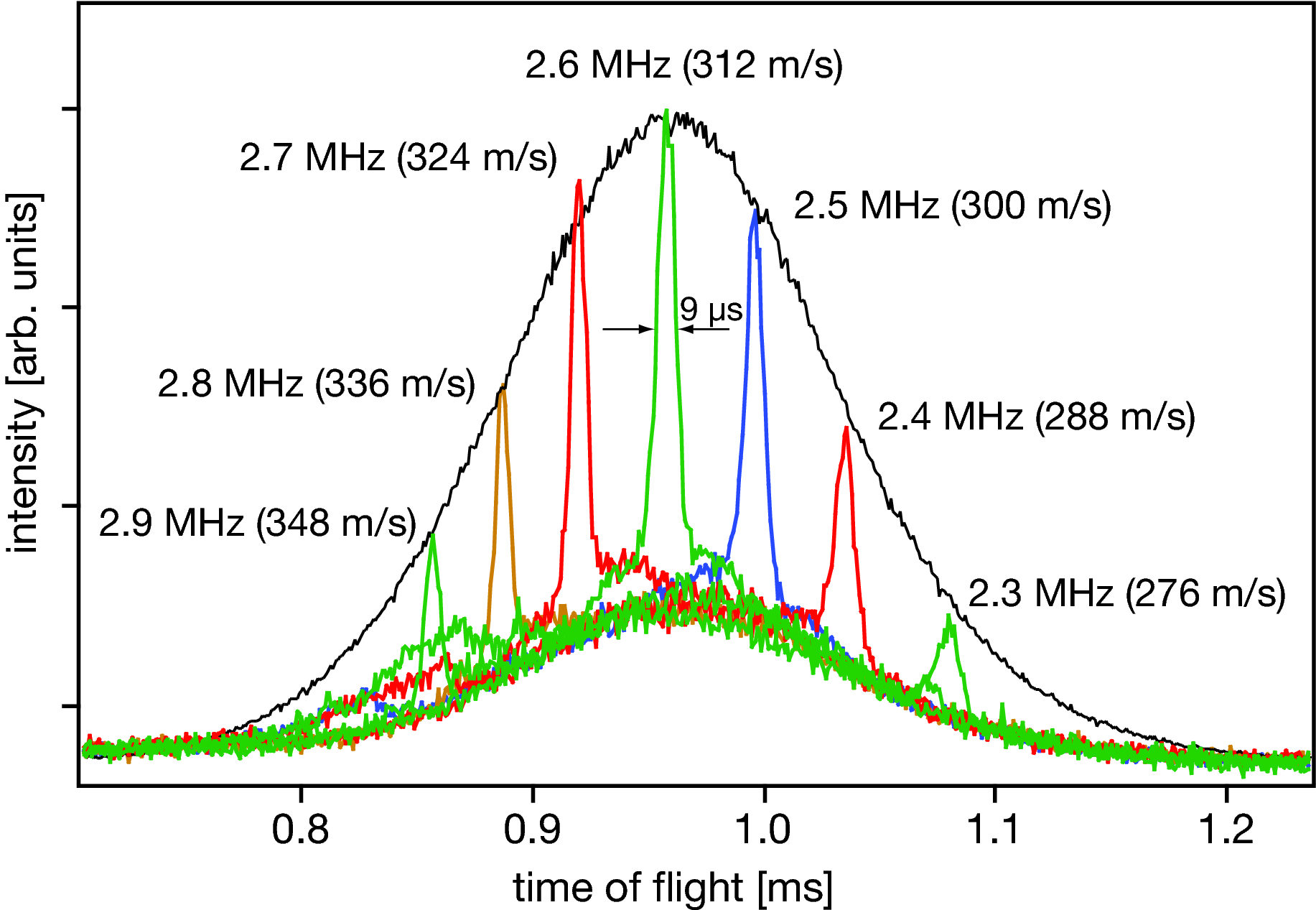
In Fig. 3, the measured arrival time distributions of metastable CO molecules are shown for seven different frequencies . The corresponding velocities of the traveling potential wells are indicated in brackets. For each frequency, a narrow peak with a FWHM of about s is observed on top of a broad pedestal. The narrow peaks originate from those metastable molecules that are actively transported along the microstructured electrode array. The width of this peak is mainly determined by the velocity spread of about m/s, corresponding to a longitudinal translational temperature of mK of the sample of guided molecules. The pedestal might be due to metastable CO molecules in low-field seeking states that pass high over the substrate and are not sufficiently deflected. It might also originate from the small fraction of metastable CO molecules in the component of the upper -doublet level in the beam, which experiences only a weak interaction with the electric field Jongma-CPL-1997 . The peak intensities of the transmitted signals for the different frequencies are determined by the intensities of the corresponding velocity groups in the original beam. This is evident from the comparison with the enveloping curve, which shows the arrival time distribution of the molecules in free flight (scaled down by more than a factor of for this comparison). The integrated intensity of the molecules guided by the MHz waveforms is count per pulse. With an estimated detector efficiency of %, this represents about metastable CO molecules from each pulse being guided in some separate minima.
The data presented here demonstrate that polar molecules from a supersonic molecular beam can be coupled into traveling potential wells on a chip. This electric conveyor belt is similar to the magnetic conveyor belt demonstrated for atoms Hansel-PRL-2001 . The six-electrode design outlined here – the analogue of which could also be implemented with magnetic fields – enables a very smooth movement of the potential wells over the chip. By decreasing the frequency of the applied waveforms while the molecules are on the chip, molecules can be decelerated and brought to a standstill. Calculations indicate that metastable CO molecules can be decelerated over a distance of mm from m/s to a standstill, a process that takes less than ms. The molecules will then be trapped in stationary potential wells above the chip. In the present design of the microstructured electrode array, the molecules are able to escape along the axis, but these holes can be plugged using additional electrodes. Once trapped, the metastable CO molecules can either be visualized using spatially resolved imaging of their phosphorescence, or they can be accelerated off the chip and detected externally. Alternatively, single molecule detection on a chip using micro-cavities can be pursued Trupke-PRL-2007 .
The operation principle of this Stark decelerator on a chip is similar to that of the Stark decelerator demonstrated originally Bethlem-PRL-1999 . However, in that configuration the electric fields are abruptly switched between two different static configurations, creating only an effective traveling potential well Bethlem-PRL-2000 ; Gubbels-PRA-2006 . The guiding and deceleration scheme presented here uses a genuine traveling potential well. This has the advantage that the molecules only experience relatively low electric fields. A scaled-up version of this structure might therefore be useful for decelerating molecules that are only low-field seeking at low electric fields, such as heavy diatomics Bethlem-JPhysB-2006 and atoms and molecules in Rydberg states Vanhaecke-JPhysB-2005 ; Softley-JESRP-2005 .
Acknowledgements.
We acknowledge discussions with S. A. Schulz during the early stages of this project. The design of the electronics by G. Heyne, V. Platschkowski, and T. Vetter and the mechanical design by H. Haak have been crucial for this work. H. L. Bethlem acknowledges financial support from the Netherlands Organisation for Scientific Research (NWO) via a VENI-grant.References
- (1) J. Fortágh and C. Zimmermann, Rev. Mod. Phys. 79, 235 (2007), and references therein.
- (2) P. Krüger, et al., Phys. Rev. Lett. 91, 233201 (2003).
- (3) T. Kishimoto, H. Hachisu, J. Fujiki, K. Nagato, M. Yasuda, and H. Katori, Phys. Rev. Lett. 96, 123001 (2006).
- (4) D. DeMille, Phys. Rev. Lett. 88, 067901 (2002).
- (5) A. André, et al., Nature Physics 2, 636 (2006).
- (6) S. A. Schulz, H. L. Bethlem, J. van Veldhoven, J. Küpper, H. Conrad, and G. Meijer, Phys. Rev. Lett. 93, 020406 (2004).
- (7) N. H. Dekker, et al., Phys. Rev. Lett. 84, 1124 (2000).
- (8) R. T. Jongma, G. von Helden, G. Berden, and G. Meijer, Chem. Phys. Lett. 270, 304 (1997).
- (9) J. J. Gilijamse, et al., J. Chem. Phys. 127, 221102 (2007).
- (10) W. Hänsel, J. Reichel, P. Hommelhoff, and T. W. Hänsch, Phys. Rev. Lett. 86, 608 (2001).
- (11) M. Trupke, J. Goldwin, B. Darquié, G. Dutier, S. Eriksson, J. Ashmore, and E. A. Hinds, Phys. Rev. Lett. 99, 063601 (2007).
- (12) H. L. Bethlem, G. Berden, and G. Meijer, Phys. Rev. Lett. 83, 1558 (1999).
- (13) H. L. Bethlem et al., Phys. Rev. Lett. 84, 5744 (2000).
- (14) K. Gubbels, G. Meijer, and B. Friedrich, Phys. Rev. A 73, 063406 (2006).
- (15) H. L. Bethlem, et al., J. Phys. B: At. Mol. Opt. Phys. 39, R263 (2006).
- (16) N. Vanhaecke, D. Comparat, and P. Pillet, J. Phys. B: At. Mol. Opt. Phys. 38, S409 (2005).
- (17) T. P. Softley, S. R. Procter, Y. Yamakita, G. Maguire, and F. Merkt, J. Electron Spectrosc. Relat. Phenom. 144, 113 (2005).