Ab initio study of transport properties in defected carbon nanotubes: an O(N) approach
Abstract
A combination of ab initio simulations and linear-scaling Green’s functions techniques is used to analyze the transport properties of long (up to one micron) carbon nanotubes with realistic disorder. The energetics and the influence of single defects (mono- and di-vacancies) on the electronic and transport properties of single-walled armchair carbon nanotubes are analyzed as a function of the tube diameter by means of the local orbital first-principles Fireball code. Efficient O(N) Green’s functions techniques framed within the Landauer-Büttiker formalism allow a statistical study of the nanotube conductance averaged over a large sample of defected tubes and thus extraction of the nanotubes localization length. Both the cases of zero and room temperature are addressed.
pacs:
73.63.Fg,72.10.Fk,73.23.-b1 Introduction
Carbon nanotubes[1, 2] are one of the most promising materials for future nanoelectronics due to their unique electrical transport properties [3]. In perfect single-walled carbon nanotubes (SWCNTs), ballistic electron conduction has been observed [4] provided inelastic processes can be neglected. In this coherent regime, however, the presence of defects, dopants or other impurities will particularly affect the performance of the device [5], as it will determine the transport in nanotubes from a ballistic regime to either weak or even strong localization regimes, where the resistance will increase exponentially with the length of the system.
To fully achieve control on the properties of carbon nanotubes, it is thus essential to perform accurate analyses of realistic disorder on carbon nanotubes-based devices. Although simulation tools based on Density Functional Theory (DFT) provide great accuracy and are particularly suitable for the study of defects in a wide range of materials, their applicability is limited by their poor scaling, which leads to a huge computational effort when the number of atoms in the system is larger than a few hundred. This prevents from using standard ab initio techniques to analyze directly the properties of electronic devices in the mesoscopic scale.
To overcome this limitation, we have combined the use of standard (no linear-scaling) first principles methods to extract the electronic properties of single defects in carbon nanotubes with the use of O(N) Green’s functions techniques to study the transport properties of long tubes with a random distribution of those defects. This approach allows to calculate characteristic transport lengths such as the localization length for different densities of defects, providing an interesting tool to tune the transport properties of carbon nanotubes, for instance, by a controlled creation of the defects [6] through irradiation, and was able to predict the existence of the Anderson localization regime in these carbon systems at room temperature as long as the electronic phase coherence is preserved [6, 7]. The emergence of the Anderson localization phenomenon in chemically doped carbon nanotubes has been theoretically predicted in other works [8, 9], in which a similar approach based on a tight-binding modeling from ab initio calculations of single B or N impurities was used to characterize the transition between different transport regimes.
2 Theoretical framework
Our analysis of the transport properties of the defected carbon nanotubes was separated into two steps. First, we studied the perturbation that single, isolated defects cause –at zero temperature– on the geometry and the electronic properties of an otherwise ideal tube. In a further step, a study of the transport properties of nanotubes with a more realistic disorder has been performed, calculating the conductance along the nanotubes, both at zero and finite temperature, for a statistically meaningful sample of nanotubes with different concentrations of randomly distributed defects.
Our approach combines first-principles calculations to obtain the effective one-electron Hamiltonian for the defected nanotubes with non-equilibrium Green’s functions techniques, which allow the calculation of the conductance for very long –up to microns– tubes.
2.1 Geometry optimization
In our calculations we have used the ab initio Fireball’96 code [10, 11, 12], that provides fast and accurate molecular dynamics calculations of the geometries and electronic properties for a wide range of systems. This method uses localized orbitals, generated by solving the atomic problem within the DFT-LDA and the pseudopotential approximations. Norm-conserving pseudopotentials are used, as well as the Ceperly-Adler form of the exchange-correlation potential as parametrized by Perdew and Zunger [13]. The forces on each atom are calculated by means of a variation of the Hellmann– Feynman theorem, and molecular dynamics are used to obtain the lowest-energy atomic configuration. A self-consistent implementation of the Harris functional allows to avoid the much time-consuming calculation of the electronic charge density , which is substituted by the calculation of the orbital occupancies of the ‘fireball’ orbitals , defined by
| (1) |
This approach allows us to optimize the electronic charge density according to the chemical environment of the atoms. The different values of are then obtained by imposing a self-consistent condition on the orbital occupancies.
In the simulations with Fireball’96 an -basis set of orbitals was used with a cut-off radius of 2.15 Å. The supercell contained 12, 10 and 6 unit cells for the , and nanotubes, respectively (the unit cell containing 20, 28 or 40 atoms for each tube). Four special k-points uniformly distributed along the first Brillouin zone of the nanotubes have been included. Convergence of the calculations is achieved for forces acting over each atom being less than 0.01 eV/Å and changes on the total energy of the system are below 10-3 eV; the time step was 0.5 fs.
2.2 Transport formalism
The calculation of the conductance has been performed within the Landauer-Büttiker formalism, more concretely in the Keldysh (non-equilibrium Green’s functions) formalism, which is particularly convenient when using a localized basis set. The differential conductance between two systems in the limit of zero temperature and low voltages is given by [14, 15]
| (2) |
where Tr[] represents the trace of operator ; describes the coupling between systems 1 and 2; and are the density of states matrices associated with the decoupled ( = 0) systems 1 and 2. Multiple scattering effects are included by means of the retarded and advanced denominator functions :
| (3) |
We are interested in calculating the conductance of a defected nanotube, but we are not including in this analysis the effect of realistic contacts. The simulation geometry will thus consist of a device region where the nanotube containing the defects is connected to two semi-infinite perfect tubes (L and R) that act as left and right electrodes (see Figure 1); the density of states of the electrodes is calculated using standard decimation techniques. The conductance along the defected region of the nanotube is calculated by an iterative procedure, starting on the left electrode L, and including at each step a random number of ideal layers of nanotube (shown as ‘…’ in Figure 1) as well as the block (supercell) of the nanotube containing the defect, and whose most stable reconstruction has been obtained using Fireball’96 (labeled as and in the same figure).

After the inclusion of a new defect, the conductance between the ‘left side’ of the system (consisting of the left lead and the increasing number of ideal and defected layers of nanotube) and the right electrode (which remains invariable during the process) is calculated. In this way, we can calculate the conductance as a function of the number of defects included (and thus of the length of the tube) for different random configuration of defects distributed along the nanotube with a given mean distance d between them. The length L of the tubes is obtained from , where is the number of defects in the nanotube.
The main advantage of this linear-scaling numerical procedure is the fact that the size of the matrices we need to invert at each step does not increase with the size of the system, but remains constant and equal to the size of the defected region of the nanotube. In this way, we can calculate the conductance for mesoscopic-size tubes with different concentrations of defects without a very expensive computational effort.
The hopping or coupling between the layers of nanotube is assumed to be the coupling between the bulk layers of ideal nanotubes. For this reason, it is essential that the number of layers included in the supercell of the ab initio simulations is large enough so that the surface layers of the supercell are not being affected by the perturbation caused by the defect and can be regarded as ‘ideal’ bulk layers.
At zero temperature, the conductance for an infinitesimal voltage is calculated just by the evaluation of the differential conductance at the Fermi level . However, at finite T there will be more states accessible to the electrons and the calculation of the conductance will be performed by means of the following expression [16]:
| (4) |
where
| (5) |
is the Fermi distribution function. In this way, the total conductance at a given temperature is calculated as the total contribution from all the electronic states included in the thermal energy window opened by the finite temperature.
3 Analysis of a single defect
Theoretical simulations [17, 18] suggest that Ar+ irradiation on carbon nanotubes will mainly create monovacancies and divacancies along the nanotube. We have therefore studied the monovacancy and the two possible orientations of the divacancy, which we will refer to as vertical (if the orientation of the chain of missing atoms is perpendicular to the nanotube direction) and lateral (if the orientation is partially parallel to the tube axis).
3.1 Monovacancies
The structural and electronic properties of vacancies-related defects in CNTs and other graphene-based materials have been extensively analyzed in the literature (see, for instance, [19, 20, 21, 22, 23, 24]). The extraction of one single atom in the nanotube leads to a metastable state, that propitiates recombination of nearest neighbors to fill the empty space left by the vacancy.
3.1.1 Effect on the geometry
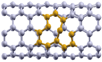
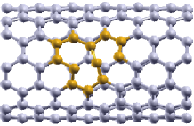
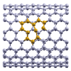
After the relaxation, we found that new bonds are formed between the neighbors of the extracted atom, favoring three-atoms against two-atoms coordination. This well-known recombination of atoms is found in the three types of armchair CNTs analyzed in this work.
The tube diameter is also affected by the extraction of the single atom. It decreases in the zone of the defect and reaches its maximum value at a distance of 5 Å from the defect, recovering the diameter of the ideal tube at the surface layer of the supercells used in our simulations. Table 1 shows diameter () for ideal tubes as well as minimum and maximum diameter for defected ones.
3.1.2 Energetics
The analysis of the energetics of the monovacancy has been performed for each CNT by means of the following difference of total energies, that allow us to compare total energies for systems containing a different number of atoms:
| (6) |
where is the total energy for an ideal tube calculated for a supercell containing the same number of layers than the supercell for the defected tube, is the total energy of the relaxed nanotube containing the monovacancy, and is the energy for the free atom. for each tube is also shown in Table 1.
| CNT | (Å) | (Å) | (Å) | (eV) |
|---|---|---|---|---|
| 6.97 | 6.56 | 7.34 | 16.62 | |
| 9.76 | 9.36 | 10.20 | 17.41 | |
| 13.89 | 13.86 | 14.76 | 17.42 |
3.2 Divacancies
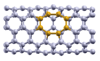
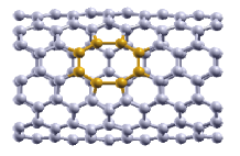
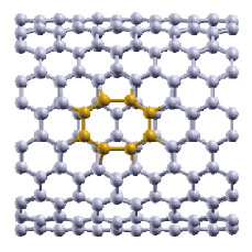
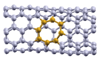
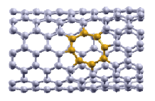
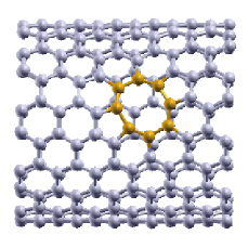
Divacancies are created extracting a second atom form the nanotube, leading to two possible orientations of the divacancy depending on which atom is extracted: removing the atom placed just above (or below) the first atom extracted will create a vertical divacancy (Figure 3), whereas the lateral divacancy is formed by the extraction of the atom located to one side of the monovacancy (Figure 4).
We have found a similar reconstructed geometry for the three CNTs analyzed: atomic relaxation leads to a new geometry formed by two pentagons and an octagon. As for the monovacancy case, the diameter decreases locally at the zone containing the defect, but the effect is much more pronounced for the case of the lateral divacancy (see Table 2).
3.2.1 Effect on the geometry
3.2.2 Energetics
The energy formation of the divacancies has been calculated in a similar way to the one performed in the case of the monovacancy. Now,
| (7) |
According to the calculated energy formation, lateral divacancies are about 2 eV more stable than vertical ones for all the analyzed nanotubes.
We can also estimate the energy for an ideal system with two monovacancies infinitely separated using
| (8) |
Comparing this energy difference with the previously calculated
| (9) |
we have found that formation of a lateral divacancy is between 6 and 7 eV more stable, for all CNTs studied, than formation of two monovacancies. Energy formation of vertical divacancies is for all tubes between 4 and 5 eV smaller than that of the lateral one when compared to the case of two isolated monovacancies. Thus, lateral divacancies formation on CNTs is preferred over that of vertical ones, and especially than formation of isolated monovacancies. Results are summarized in Table 2.
| CNT | (Å) | (Å) | (Å) | (eV) |
|---|---|---|---|---|
| vertical divacancy | 6.97 | 6.99 | 7.19 | 4.3 |
| lateral divacancy | 6.97 | 6.64 | 7.28 | 6.5 |
| vertical divacancy | 9.76 | 9.72 | 9.99 | 4.8 |
| lateral divacancy | 9.76 | 9.36 | 10.02 | 6.7 |
| vertical divacancy | 13.89 | 13.88 | 14.07 | 4.2 |
| lateral divacancy | 13.89 | 13.72 | 14.65 | 6.7 |
3.3 Scattering of a single defect at zero temperature
Although a large number of theoretical works have been performed to analyze the scattering produced by single defects (either topological or substitutional impurities), it is worth mentioning that a full relaxation of the atomic region around the defect is particularly important in the case of vacancies, where the energetically more stable reconstructed vacancy will present a different electronic structure than the ideal (non-reconstructed) one, leading to a very different behavior of the conductance and other transport properties, especially for energies close to the Fermi level.
In the case of a tight-binding model [25], a monovacancy in an armchair CNT will produce a drop of almost one conductance quantum, G, right at the Fermi level, with the electron-hole symmetry fully preserved. The conductance of a single ideal monovacancy, that is, in the metastable non-reconstructed state, will as well lead to a drop of almost , not at the Fermi level but somewhat below at the valence band, as shown in Figure 5 (where the Fermi energy has been set to zero). This result agrees with previous ab initio calculations [26, 27].
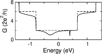
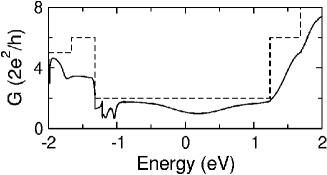
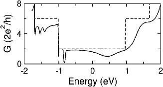
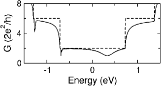
However, the situation is very different in the case of the most stable reconstruction. Figure 6 shows the conductance as a function of the energy for the , and nanotubes with a single monovacancy after relaxation. Rearrangement of atoms has propitiated the saturation of dangling bonds, and the reconstructed nanotube presents a conductance much more similar to the ideal case for low energy than that of the metastable monovacancy. Particularly, there is a very small drop in the conductance for energies in the vicinity of the Fermi level, and the narrow peaks in the conduction band due to the unsaturated bonds that are present for the non-reconstructed geometry have disappeared.
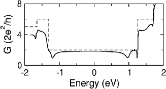
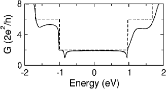
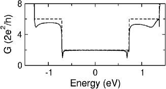
As expected, the drop in the conductance decreases with increasing diameter of the nanotubes, being practically negligible for the tube. This is in good agreement with previous calculations [28, 27]
The drop of the conductance is much larger for both orientations of the divacancy. In all cases a maximum drop of about one conductance quantum is found for the two orientations of the divacancy. This is also in agreement with previous works [23].
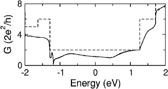
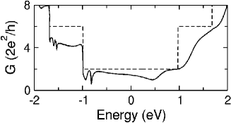
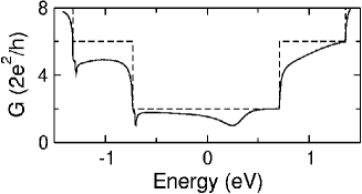
As lateral divacancies are much more stable than the vertical ones, and due to small drop in the conductance caused by monovacancies, the results we present include only lateral divacancies.
4 Statistical analysis
Once the transport properties of the isolated defects in the infinite nanotube have been characterized, we are interested in calculating the conductance along a more realistic nanotube in which defects can be randomly distributed along and around the axis of the tube. Lateral divacancies are distributed along the tube with the distance between consecutive defects presenting a uniform random distribution between 0 and 2d –d thus being the mean distance between defects for a particular defect density. The calculation of the resistance (as the inverse of the differential conductance) for each particular random distribution of defects has been performed as explained in Section 2.2.
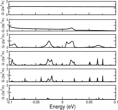
For each particular distribution of defects we can calculate the conductance as a function of energy according to (4). In Figure 9 we plot the conductance around a small energy region around the Fermi level for the nanotube and a mean distance between defects of d = 10.1 nm for different number of defects included in the nanotube. The nanotube conductance presents strong fluctuations, with a maximum value close to the conductance quantum and a minimum that becomes smaller for an increasing number of divacancies. In fact, conductance never crosses the critical value of one conductance quantum once a certain number of defects have been included. This result can be very clearly seen in Figure 10, where the conductance never reaches values higher than 1 G0 after N = 5 [7].
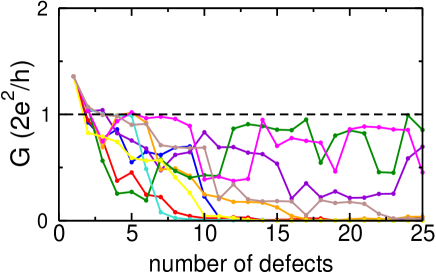
To clarify this issue, we have diagonalized the transmission matrix [30] to calculate the conductance for each one of the two conduction channels existing for energies around the Fermi level. According to this, only one of the two conduction channels is contributing to the total conductance once a number of 5-9 divacancies are presented in the nanotube. The origin of this channel suppression remains, however, unclear.
The appropriately averaged resistance –according to the theory of disordered one-dimensional systems [29]– for a statistically significant number of random configurations of defects (up to 100 in the case of zero temperature, and up to 15 for the room temperature case, where the dispersion with respect to the mean value is much smaller) has been calculated for mean distances d between 10.1 nm and 75.5 nm.
Figure 11 shows the resistance, for the CNT, of a selected number of the calculated random distributions of defects at both zero and room temperature. Curves with the same color in (left) and (right) plots correspond to the same configuration of defects.
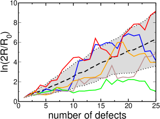
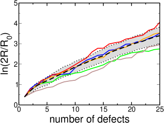
At zero temperature, the resistance for each defect realization strongly fluctuates along the nanotube length, showing the characteristic behavior of disordered 1D system. The average resistance, however, presents a clear exponential behavior as a function of the length, which is a typical feature of strongly localized systems. At room temperature, resistance fluctuations disappear for increasing values of T, leading to very smooth curves when a critical temperature (scaling with 1/d) is reached, but preserving the exponential behavior. This fact confirms the presence of the Anderson localization regime at room temperature for the defected nanotubes studied. This result has been confirmed by experimental data [6, 31].
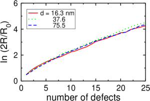
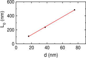
Figure 12 shows the averaged resistance for different mean distances at room temperature for the nanotube. For all defect densities studied we have found the strongly localized regime and the exponential increase of the resistance as a function of the tube length. We can then fit the average resistance for every d to the expression
| (10) |
where L is the length of the nanotube calculated as L = N d and L0 is the localization length. In this way we can calculate the localization length L0 for every defect density. These results for the nanotube are summarized in Figure 12 (right). A detailed analysis of the methodology and theoretical results obtained at different temperatures, as well as the experimental data supporting these conclusions, can be found in references [6, 7] for the and in [31] for the .
5 Conclusions
In summary, we have analyzed, by means of a combination of ab initio simulations and linear-scaling Green’s functions techniques, transport properties of armchair , and carbon nanotubes with realistic disorder, namely mono- and di-vacancies. In a first step, first-principles simulations for each defect have been performed in order to determine the most stable reconstructions. The conductance profile for every defect has been then analyzed. Our results show that reconstructed monovacancies present an almost negligible drop of the nanotube conductance at the Fermi level compared to that of divacancies. As the lateral orientation of the divacancy is found to be about 2 eV more stable than the vertical one for all the nanotubes considered, only lateral divacancies have been included in our analysis of long tubes with different defect densities. Using an O(N) recursive procedure based on standard Green’s functions techniques we have calculated the localization length for several defect densities, predicting the existence of the Anderson localization regime for defected carbon nanotubes at room temperature.
References
References
- [1] S. Iijima, Nature 354, 56 (1991)
- [2] J.-C. Charlier, X. Blase and S. Roche, Rev. Modern. Phys. 79, 677 (2007) and references therein.
- [3] F. Banhart, Rep. Prog. Phys. 62, 1181 (1999); M. P. Anantram and F. Léonard, Rep. Prog. Phys. 69, 507 (2006);
- [4] W. Liang, M. Bockrath, D. Bozovic, J.H. Hafner, M. Tinkham and H. Park, Nature 411, 665 (1991); S. Frank, P. Poncharal, Z.L. Wang and W.A. de Heer, Science 280, 1744 (1998); A. Bachtold, C. Strunk, J.-P. Salvetat, J.-M. Bonard, L. Forró, T. Nussbaumer and C. Schönenberger, Nature 397, 673 (1999); A. Javey, J. Guo, Q. Wang, M. Lundstrom and H.J. Dai, Nature 424, 654 (2003); J.Y. Park, S. Rosenblatt, Y. Yaish, V. Sazonova, H. Ustünel, S. Braig, T.A. Arias, P.W. Brouwer and P.L. McEuen, Nano Lett. 4, 517 (2004);
- [5] M. Bockrath, W. Liang, D. Bozovic, J.H. Hafner, C.M. Lieber, M. Tinkham, and H. Park, Science 291, 283 (2001); A. Hashimoto, K. Suenaga, A. Gloter, K. Urita, S. Iijima, Nature 430, 870 (2004)
- [6] C. Gómez-Navarro, P.J. de Pablo, J. Gómez-Herrero, B. Biel, F.J. García-Vidal, A. Rubio and F. Flores, Nature Mat. 4, 534 (2005)
- [7] B. Biel, F.J. García-Vidal, A. Rubio and F. Flores, Phys. Rev. Lett. 96, 266801 (2005)
- [8] S. Latil, S. Roche, D. Mayou, and J.-C. Charlier, Phys. Rev. Lett. 92, 256805 (2004);
- [9] R. Avriller, S. Latil, F. Triozon, X. Blase and S. Roche Phys. Rev. B 74, 121406 (2006)
- [10] O.F. Sankey and D.J. Niklewski, Phys. Rev. B 40, 3979 (1989)
- [11] A. Demkov, J. Ortega, O.F. Sankey and M.P. Grumbach, Phys. Rev. B 52, 1618 (1995)
- [12] J. Ortega, Comput. Mat. Sci. 12, 192 (1998)
- [13] J. Perdew and A. Zunger Phys. Rev. B 23, 5048 (1981)
- [14] A. Martín-Rodero, F. Flores and N. H. March, Phys. Rev. B 38, 10047 (1988)
- [15] N. Mingo, L. Jurczyszyn, F. García-Vidal, R. Sáiz-Pardo, P. de Andrés, F. Flores, S. Wu and W. More, Phys. Rev. B 54, 2225 (1996)
- [16] M. Büttiker, Y. Imry, R. Landauer and S. Pinhas, Phys. Rev. B 31, 6207 (1985)
- [17] A.V. Krasheninnikov, K. Nordlund, M. Sirvio, E. Salonen and J. Keinonen, Phys. Rev. B 63, 245405 (2001)
- [18] A.V. Krasheninnikov, K. Nordlund and J. Keinonen, Phys. Rev. B 65, 165423 (2002)
- [19] P.M. Ajayan, V. Ravikumar, J.-C. Charlier, Phys., Rev. Lett. 81, 1437 (1998);
- [20] C.P. Ewels, M.I. Heggie and P. R. Briddon, Chem. Phys. Lett. 351, 178 (2002)
- [21] A.J. Lu and B.C. Pan, Phys., Rev. Lett. 92, 105504 (2004);
- [22] J. Kotakoski, A.V. Krasheninnikov and K. Nordlund, Phys. Rev. B 74, 245420 (2006)
- [23] R.G. Amorim, A. Fazzio, A. Antonelli, F.D. Novaes and A.J.R. da Silva, Nano Lett. 7, 2459 (2007)
- [24] H. Amara, S. Latil, V. Meunier, Ph. Lambin and J.-C. Charlier, Phys. Rev. B 76, 115423 (2007)
- [25] L. Chico, L. X. Benedict, S.G. Louie and M.L. Cohen, Phys. Rev. B. 54, 2600 (1996)
- [26] H.J. Choi, J. Ihm, S. G. Louie and M. L. Cohen,, Phys. Rev. Lett. 84, 2917 (2000)
- [27] Y.W. Son, M.L. Cohen and S.G. Louie, Nano Lett. 7, 3518 (2007)
- [28] M. Brandbyge, J.-L. Mozos, P. Ordejón, J. Taylor and K. Stokbro, Phys. Rev. B 65, 165401 (2002)
- [29] J.B. Pendry, Adv. Phys. 43, 461 (1994)
- [30] P. Jelínek, R. Pérez, J. Ortega and F. Flores, Phys. Rev. B 68, 085403 (2003)
- [31] F. Flores, B. Biel, A. Rubio, F.J. García-Vidal, C. Gómez-Navarro, P.J. de Pablo and J. Gómez-Herrero, J. Phys: Condens. Matter (in press)