Quantum fluctuations in ultranarrow superconducting nanowires
Abstract
Progressive reduction of the effective diameter of a nanowire is applied to trace evolution of the shape of superconducting transition in quasi-one-dimensional aluminum structures. In nanowires with effective diameter 15 nm the dependences are much wider than predicted by the model of thermally activated phase slips. The effect can be explained by quantum fluctuations of the order parameter. Negative magnetoresistance is observed in the thinest samples. Experimental results are in reasonable agreement with existing theoretical models. The effect should have a universal validity indicating a breakdown of zero resistance state in a superconductor below a certain scale.
pacs:
74.25.Fy, 74.40.+k, 74.78.-w, 74.62.-c
I
Introduction
The ability to carry a dissipationless electric current is a fundamental attribute of a superconductor. One might naively expect that this property is preserved at reduced dimensions. Unfortunately, inevitable fluctuations result in momentary suppression of superconductivity leading to energy dissipation. Being integrated in time, this effect manifests itself as finite resistance. Of particular interest are quasi-one-dimensional (quasi-1D) systems, with effective diameter smaller than the superconducting coherence length , where there is only one parallel channel of supercurrent. In such objects, due to fluctuations of the order parameter, the effective resistance is never strictly equal to zero. However, a measurable resistance at temperatures well below the critical temperature can be observed only in samples with rather small diameters. Early experiments R(T)of tin whisker confirmed that in narrow superconducting channels the shape of the transition can be explained by thermal fluctuations Langer . Recent experimental Giordano - Altomare and theoretical Duan - Pesin discoveries claim the existence of an additional (non thermal) mechanism of finite resistance in 1D systems. The issue is of vital importance for the development of superconducting nanoelectronic elements designed to carry a dissipationless electric current.
The finite resistance of a 1D channel can be understood that for sufficiently longs system of length there is always the finite probability of a fluctuation to drive instantly a fraction of the wire of volume into a normal state. The energy required for this process is the corresponding superconducting condensation energy , where is the critical magnetic field. If thermal effects solely contribute to the fluctuations, it has been shown Langer that the effective dc voltage is proportional to the probability of these events , where is the Boltzman constant:
| (1) |
is the temperature-dependent critical current, and with being the superconducting flux quantum. The current dependence is determined by the term and the term under the exponent, responsible for the effective reduction of the potential barrier by the finite current . An exact form of the pre-factor has been proposed Langer . Though the function also contains temperature- and current-dependent terms, it contributes negligibly compared to the strong exponential dependence. Formally the above process can be described as the thermally activated transition of a superconducting system from a local potential minimum to a neighboring one separated by in phase space: so called, thermally activated phase slip (TAPS). One can make a formal analogy with a ”classical jump” of a particle over the barrier stimulated by the thermal energy .
An alternative mechanism has been proposed associated with tunneling through the energy barrier in phase space Giordano . Such tunneling to a state of lower energy, also called quantum phase slip (QPS), should provide an additional (to TAPS) channel of energy dissipation in a current carrying system. For conventional type-I superconductors estimations show that measurable deviations from the TAPS mechanism are expected in samples with effective diameter 10 nm. There have been a few experiments, claiming observation of QPS phenomenon in various superconducting materials: In, Pb and Pb-In Giordano , Pb, Sn and Pb-Bi Sharifi , MoGe Bezryadin , Sn and Zn Tian , Al Zgirski NanoLett , Altomare . Various models consider non-thermal mechanisms of the finite resisitivity of a 1D superconductor Saito - Pesin . In spite of the intensive research in the field, the matter is far from being settled. From an experimental point of view, to some extent, the inhomogeneity of a nanowire might lead to a broad superconducting transition which can be erroneously associated with the QPS mechanism Zgirski PRB limitation . Another source of misinterpretation might come from insufficient filtering from environmental RF noise. The resulting parasitic overheating can shift the superconducting transition to lower temperatures, distorting the shape of the dependence.
Our motivation was to perform experiments eliminating the uncertainty related to the uniqueness of each particular nanostructure. We were able to trace the crossover from the TAPS mechanism to QPS in the same sample , successively reducing its diameter between measurements, thereby evidencing for a solely size dependent origin of the phenomenon. The experiments performed on multiple sets of aluminum nanowires reduced by ion sputtering down to sub-10 nm scales showed quantitatively similar behavior. In all structures with effective diameter 15 nm the dependences deviate from the predictions of the TAPS model Langer , while the QPS scenario Zaikin provides a reasonable fit to the data.
II
Experiment
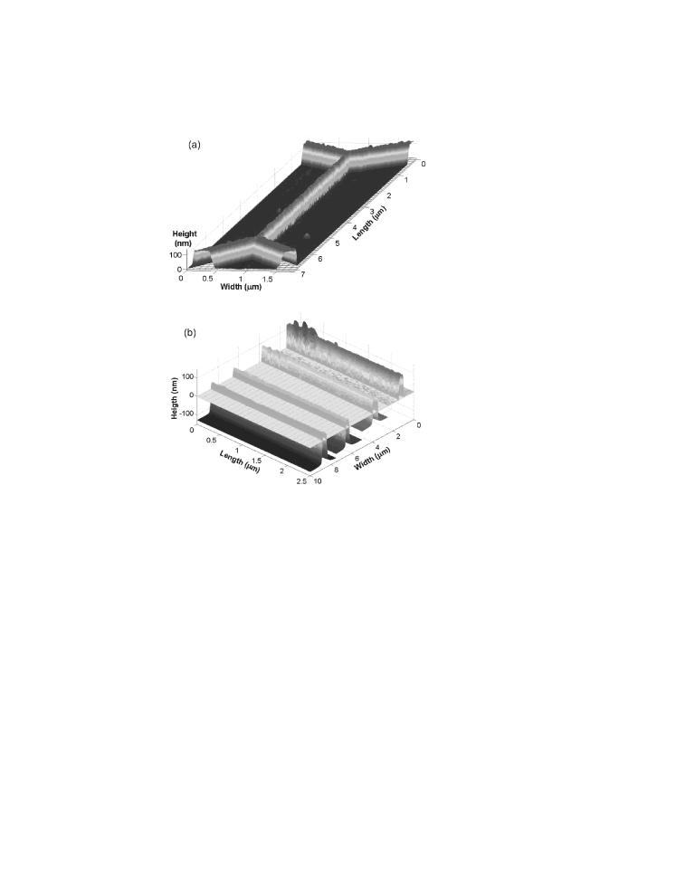
In our earlier work ion sputtering we demonstrated that low energy ion sputtering progressively and non-destructively reduces nanostructure dimensions. The penetration depth of ions into an matrix at acceleration voltages of 500 eV is about 1.5 nm and is comparable to the thickness of naturally formed oxide. The accuracy of the effective diameter determination from the normal state resistance, scanning electron microscope (SEM) and scanning probe microscope (SPM) measurements is about 2 nm. Only those samples which showed no obvious geometrical imperfections were used for further experiments. While reducing the nanowire diameter, the low energy ion sputtering also provides ”polishing” removing surface roughness inevitable after a lift-off process Zgirski NanoLett (Fig. 1). In this work the method ion sputtering , Zgirski Nanotechnology 2008 was applied to lithographically fabricated 99.999 % pure nanowires with initial cross-section of about 100 nm x 100 nm. During measurements the structures were immersed into a directly pumped bath with base temperature of about 0.95 K. Contrary to Refs. Bezryadin , Tian , Altomare , we used a four-probe configuration, eliminating necessity to consider the contribution of the electrodes. We obtained exact quantitative agreement between data measured with dc and ac currents using extensive multistage rf filtering. The results are reproducible and do not suffer from hardware-related artifacts.
III
Results and discussion
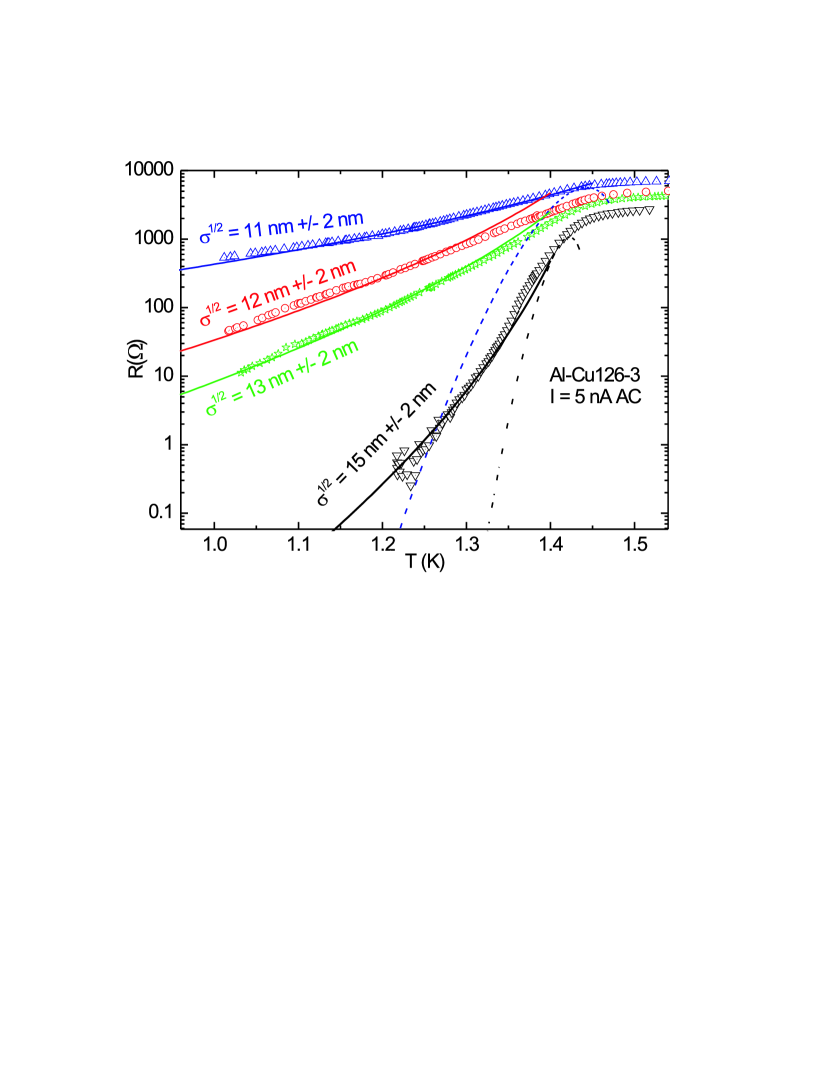
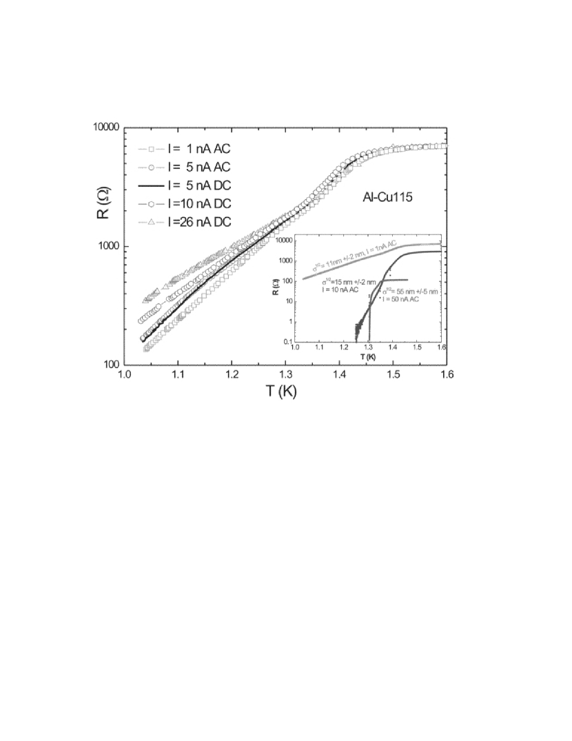
After a sequence of sputterings [alternated with measurements] the wire cross section is reduced down to 20 nm, where deviations from TAPS behavior become obvious (Fig. 2). Similar results were obtained on several sets of aluminum nanowires with length equal to 1 , 5 and 10 . For larger diameters (e.g., Fig. 3, insert, 55 nm wire) the shape of the R(T) dependence can be qualitatively described by the TAPS mechanism. Notice that a size dependent variation of the critical temperature of a nanowire Shanenko , especially pronounced in aluminum Zgirski NanoLett , results in a broadening of the transition and significantly reduces straightforward applicability of the TAPS model Zgirski PRB limitation . Confidence in assigning our results to the manifestation of a new (non-thermal) mechanism comes from the experimental observation that in aluminum nanowires (films) the critical temperature increases with a decrease of the wire diameter (film thickness) Shanenko , Zgirski NanoLett . It means that the broadening of the dependencies below the bulk value 1.2 K cannot be explained by a geometrical imperfection (e.g., constriction) of an aluminium nanowire. Below a certain limit 20 nm fits by the TAPS model fail to provide any reasonable quantitative agreement with experiment even assuming the existence of unrealistically narrow constrictions not observed by SPM (Fig. 2).
Though several theoretical approaches Saito - Pesin were proposed to describe the non-TAPS mechanism of finite resistance in 1D superconducting channels, not all models are suitable for direct comparison with experiment, lacking a clear expression for the resistance (voltage) as a function of temperature. Where possible, we tried to compare our data with the models and found the best agreement with renormalization theory Zaikin . The full version of the model for systems of an arbitrary length is rather sophisticated, requiring knowledge of parameters not easily deductible from experiment. However, if the wire is short enough that only one phase slip event can happen at a time, one can neglect the effects of the interaction between the phase slips. In this limit the simplified expression for the rate of QPS activation is
| (2) |
where the action , with being a numerical constant, 6.47 and is the characteristic response time of a superconducting system which roughly determines the duration of each QPS Zaikin . The effective (time averaged) voltage due to the fluctuations can be found using the Josephson relation Langer . Finally, for the effective resistance of a quasi-1D superconducting nanowire one gets
| (3) |
Contrary to TAPS Langer , the QPS contribution has a rather weak temperature dependence far from the critical temperature and should produce a finite resistance even at for sufficiently narrow wires Zaikin . One can achieve reasonable agreement between the model [Eqs. 2 and 3] and the experiment (Fig. 2). There are four fitting parameters: critical temperature , normal state resistance , mean free path [to re-calculate the dirty limit coherence length ], and the numerical parameter of the order of unit Zaikin . The critical temperature and the normal state resistance can be trivially deduced from experimental dependences. Roughly the mean free path can be estimated from the normal state resistivity , as the product is a well-tabulated value for dirty-limit aluminum. In our ultra-narrow nanowires the cross-section is known from SPM measurements with 2 nm accuracy. Hence, there is some freedom in the selection of the mean free path. As a rule of thumb for all our nanowires with effective diameter 20 nm the best-fitted mean free path (at low temperatures) was found to be roughly equal to one-half of the diameter (Fig. 2, caption). The observation is quite reasonable, taking into consideration that at these scales and temperatures electron scattering is mainly determined by the sample’s physical boundaries. For all aluminum nanowires the best-fitted value for the parameter was found to be equal to 0.15. As the value of cannot be calculated within the model Zaikin with the required accuracy, we believe that the correspondence between the simplified ”short wire” model and the experiment can be considered as good.
No Coulomb blockade has been observed on characteristics, indicating good homogeneity of the wires (absence of tunnel barriers). Below the critical temperature dependences show behavior similar to both TAPS [Eq. 1[] and renormalization Zaikin models. At sufficiently small currents 20 nA one might expect a linear response, while at much higher currents trivial overheating is observed. However, there exist an intermediate regime between linear and strongly non-linear regimes: the top part of the transition is not shifted, while the slope of the bottom part decreases with an increase of the measuring current (Fig. 3). We associate this peculiarity with the reduction of the potential barrier by a finite current [Eq. 1], which is qualitatively similar for thermal Langer and quantum Zaikin mechanisms.
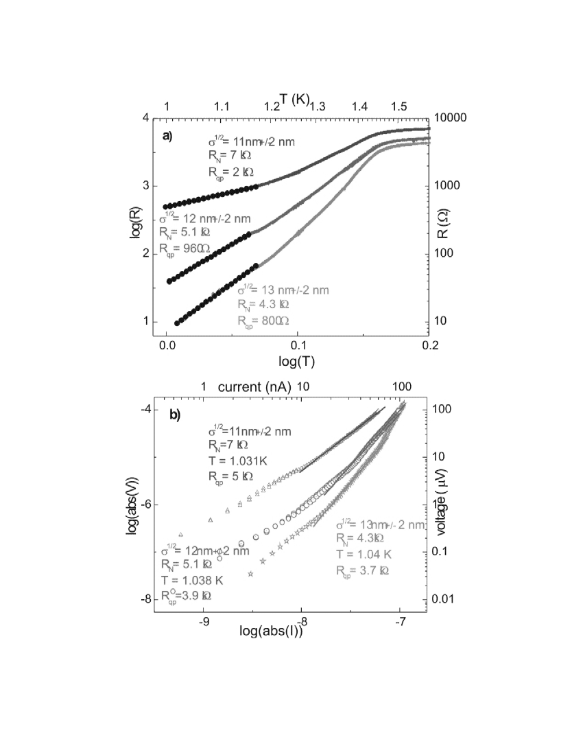
At certain limits the renormalization model Zaikin predicts the same functional dependence of the effective resistance on temperature and current. In the high temperature limit , , and in the high current limit , . The dimensionless conductance is related to the effective ”quasiparticle” resistance , being associated with dissipation provided by the quasiparticle channel. can be considered as a fitting parameter and should be of the order of the normal state resitance . In the metallic phase, when quantum fluctuations dominate the behavior of the system, the residual resistance at should correspond to Zaikin . The results of fitting of our and dependences to the above relations are presented in Fig. 4. One may obtain satisfactory agreement with experimental data, allowing the quasiparticle resistance to be smaller than the normal state resistance of the nanowire. For each sample, the deviation of the fitting parameter from is less pronounced for characteristics. Probably, this discrepancy is the result of the experimental difficulty to satisfy the applicability condition , while the temperature should be noticeably below the critical temperature , where the whole concept of phase slippage is valid.
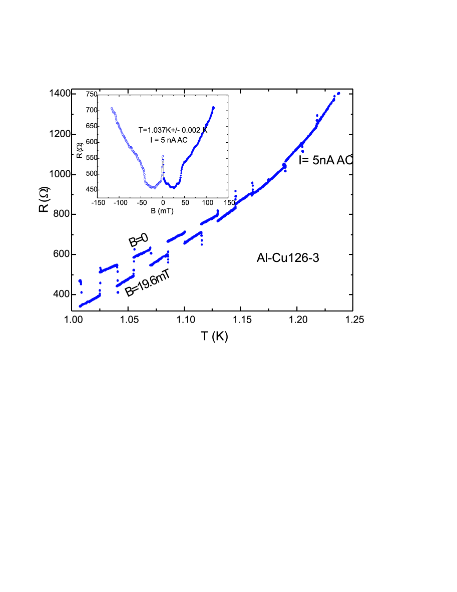
Application of a magnetic field perpendicular to the plane of the structures reveals a rather unusual effect. At sufficiently small temperatures a pronounced negative magnetoresistence (nMR) is observed (Fig. 5, inset), resulting in a ”sharpening” of the transitions in magnetic fields 25 mT (Fig. 5). nMR is observed only in the thinest samples 20 nm and only at temperatures well below the onset of superconductivity. A similar effect has been reported for ultrathin 1D lead strips Sharifi . Aluminum is known to be immune to the creation of localized magnetic moments provided by the majority of magnetic elements. Our samples were e-beam evaporated from 99.999 % pure aluminum target in an UHV chamber where magnetic materials have never been processed. Hence, the residual concentration of magnetic ions should be negligible. Even if we were to assume their presence, magnetic fields where nMR is observed are too small to polarize them. Additionally, we do not see an enhancement of related to the onset of superconductivity, which would be the consequence of suppression of the Kondo mechanism by a magnetic field. As the presence of localized magnetic moments in our samples is not obvious, a recently developed model of nMR Ref. Bezryadin nMR is not applicable. nMR has been predicted in disordered superconducting wires Pesin . However, the main result of that model is an exponentially small addition to the TAPS effective resistance. This conclusion contradicts our main observation (Fig. 2) and, hence, the applicability of the whole model Pesin to our experiments is questionable. For the moment we do not have a solid explanation for the nMR effect. The phenomenon might be related to an interplay between two field-dependent contributions: barrier reduction and suppression of the superconducting energy gap . The first process provides an expected increase of the observed resistance, while the second one leads to a reduced quasiparticle resistance due to thermal activation of extra quasiparticles resulting in lower effective resistance . There might be a region of magnetic fields where the second mechanism ”wins” reducing the influence of quantum fluctuations leading to nMR Zaikin . Another explanation of the nMR might be related to the formation of a charge imbalance region accompanying each phase slip event Arutyunov nMR . This non-equilibrium region provides dissipation outside the core of a phase slip. The corresponding Ohmic contribution can be effectively suppressed by the magnetic field, resulting in nMR. However, so far the validity of the charge imbalance concept was only demonstrated at temperatures sufficiently close to and its applicability to QPS at temperatures well below the critical one is not obvious. A quantitative comparison with the experiments requires further elaboration of the theory.
IV
Conclusions
The homogeneity of the wires is the central point in an interpretation of data related to phase slip mechanisms: thermal or quantum. The existence of trivial structural or geometrical imperfections as constrictions, boundaries and contact regions might broaden the dependences Zgirski PRB limitation and can be erroneously interpreted as a ”new physic”’. The specially developed method of ion beam sputtering ion sputtering , Zgirski Nanotechnology 2008 to a large extent allowed us to study the evolution of the size phenomenon, eliminating artifacts related to the uniqueness of samples fabricated in independent processing runs. The ion beam treatment polishes the surface of the samples, removing the inevitable roughness just after fabrication (Fig. 1). If there were no detectable geometrical imperfections in the original (thick) wires, they cannot be introduced while reducing the diameter by the low energy ion sputtering. Formally, it cannot be excluded that in the original structures there were ”hidden” undetectable structural defects (e.g., highly resistive grain boundaries) which did not contribute to conductivity, being shunted by the bulk. When the diameter of the wire is reduced below a certain scale, this type of imperfections might determine the behavior of the quasi-1D system. However, the absence of Coulomb blockade and/or gap structure on characteristics rules out the presence of the highly resistive tunnel barriers.
The extensive SPM and SEM analysis indicates that after several sessions of ion beam sputtering the surface of our nanowire is flat with few nm accuracy Zgirski Nanotechnology 2008 . This is quite small in absolute terms, particularly keeping in mind that the lattice constant in aluminum is 0.4 nm. However, approaching the 10 nm scale, a few nm roughness means a lot in relative terms. Hence, we cannot exclude the possibility that the specified average effective diameter of our nanowires is not very representative: the phase slippage might happen in the weakest (thinnest?) parts. To eliminate completely this uncertainty one should study infinitely long atomically flat structures, which are quite problematic to fabricate. Nevertheless, the main conclusion of the present paper is still valid even assuming the presence of inevitable imperfection of the samples. At all realistic parameters characterizing the geometry of the possible constrictions, the thermal activation scenario Langer fails to explain the broad dependences observed in sub-15 nm nanowires, while the QPS mechanism Zaikin provides good agreement with the experiment (Fig. 2).
In conclusion, we have traced the evolution of the shape of the superconducting transition in quasi-one-dimensional aluminum nanowires with progressive reduction of their cross-sections. For relatively thick samples 20 nm the shape of the transitions can be qualitatively explained in terms of wire inhomogeneity and the model of thermally activated phase slips (TAPS). While in nanowires with effective diameter 15 nm the dependences are much wider and no reasonable set of fitting parameters can account for the TAPS mechanism. The phenomenon is associated with manifestation of quantum fluctuations of the order parameter. The results are in good agreement with renormalization theory Zaikin . The effect of quantum fluctuations should have a universal validity, indicating a breakdown of the zero resistance state in quasi-one-dimensional superconductors, setting fundamental limitations on miniaturization of nanoelectronic components designed to carry a dissipationless supercurrent.
V
Acknowledgments
The authors would like to acknowledge C. N. Lau, A. Bezryadin, D. Golubev, L. Pryadko, A. Zaikin, and D. Vodolazov for their helpful discussions. The work was supported by the EU Commission FP6 NMP-3 project 505457-1 ULTRA-1D ”Experimental and theoretical investigation of electron transport in ultranarrow 1-dimensional nanostructures”.
References
- (1) Lukens, J. E., Warburton, R. J. and Webb, W.W. ,Phys. Rev. Lett. 25, 1180-1184 (1970); R. S. Newbower, M. R. Beasley and M. Tinkham, Phys. Rev. B 5, 864-868 (1972).
- (2) Langer, J.S. and Ambegaokar, V. Phys. Rev. 164, 498-510 (1967); McCumber, D.E. and Halperin, B.I., Phys. Rev. B 1, 1054-1070 (1970).
- (3) N. Giordano, Phys. Rev. Lett. 61, 2137 (1988), N. Giordano and. E.R. Schuler , Phys. Rev. Lett. 63, 2417 (1989), N. Giordano, Phys. Rev. B. 41, 6350 (1990), Phys. Rev. B. 43, 160 (1991), Physica B 203, 460-466 (1994).
- (4) Sharifi, F., Herzog, A.V., and Dynes, R. C., Phys. Rev. Lett. 71, 428 (1993); A. V. Herzog, P. Xiong, F. Sharifi, and R.C. Dynes, Phys. Rev. Lett. 76, 668 (1996); P. Xiong, A. V. Herzog, and R.C. Dynes Phys. Rev. Lett. 78, 927 (1997)
- (5) Bezryadin, A., Lau, C.N., Tinkham, M., Nature 404, 971(2000); C. N. Lau, N. Markovic, M. Bockrath, A. Bezryadin, and M. Tinkham, Phys. Rev. Lett. 87, 217003 (2001); M. Tinkham and C. N. Lau , Appl. Phys. Lett. 80, 2946 (2002); M. Tinkham, C. N. Lau, N. Markovic, Physica E 18, 308 (2003); N. Markovic, C.N. Lau, M. Tinkham, Physica C 387, 44 (2003); A.T. Bollinger, A. Rogachev, M. Remeika, and A. Bezryadin, Phys. Rev. B 69, 180503 (2004); A. Rogachev, A.T. Bollinger, and A. Bezryadin, Phys. Rev. Lett. 94, 017004 (2005).
- (6) Mingliang Tian,Jinguo Wang, Joseph Snyder, James Kurtz, Ying Liu, Peter Schiffer, Thomas E. Mallouk, and M. H. W. Chan, Appl. Phys. Lett. 83, 1620 (2003); Mingliang Tian, Jinguo Wang, James S. Kurtz, Ying Liu, and M. H. W. Chan, Theresa S. Mayer, Thomas E. Mallouk, Phys. Rev. B 71, 104521 (2005); Mingliang Tian, Nitesh Kumar, Shengyong Xu, Jinguo Wang, James S. Kurtz, and M. H. W. Chan, Phys. Rev. Lett. 95, 076802 (2005).
- (7) M. Zgirski, K. P. Riikonen, V. Touboltsev, and K. Arutyunov, Nano Lett. 5, 1029 (2005).
- (8) Fabio Altomare, A. M. Chang, Michael R. Melloch, Yuguang Hong, and Charles W. Tu, Phys. Rev. Lett. 97, 017001 (2006).
- (9) S. Saito and Y. Murayama, Phys. Lett. A 153, 55 (1989).
- (10) J.-M. Duan, Phys. Rev. Lett. 74, 5128 (1995).
- (11) A.D. Zaikin, D. S. Golubev, A. van Otterlo, and S. T. Zimanyi, Phys. Rev. Lett. 78, 1552 (1997); Usp. Fiz. Nauk 168, 244 (1998); D. S. Golubev and A.D. Zaikin, Phys. Rev. B 64, 014504 (2001).
- (12) Y. Chang, Phys. Rev. B 54, 9436 (1996).
- (13) Y. Oreg and A. M. Finkel’stein, Phys. Rev. Lett. 83, 191 (1999).
- (14) R. A. Smith, B. S. Handy, and V. Ambegaokar, Phys. Rev. B 63, 094513 (2001).
- (15) G. Refael, E. Demler, Y. Oreg, D. S. Fisher, Phys. Rev.B 68, 214515 (2003).
- (16) H.P. Buchler, V. B. Geshkenbein, and G. Blatter, Phys. Rev. Lett. 92, 067007 (2004).
- (17) S. Sachdev, P. Werner, and M. Troyer, Phys. Rev. Lett. 92, 237003 (2004).
- (18) S. Khlebnikov, Phys. Rev. Lett. 93, 090403 (2004); S. Khlebnikov and L. Pryadko, Phys. Rev. Lett. 95, 107007 (2005).
- (19) D.A. Pesin and A. V. Andreev, Phys. Rev. Lett. 97, 117001 (2006)
- (20) M. Zgirski and K. Yu. Arutyunov, Phys. Rev. B, 75, 172509 (2007).
- (21) Savolainen, M., Touboltsev, V., Koppinen, P., Riikonen, K.-P., and Arutyunov., K. Appl. Phys. A 79, 1769 (2004).
- (22) A. A. Shanenko, M. D. Croitoru, M. Zgirski, F. M. Peeters, and K. Yu. Arutyunov, Phys. Rev. B 74, 052502 (2006).
- (23) A. Rogachev, T.-C. Wei, D. Pekker, A. T. Bollinger, P.M. Goldbart, and A. Bezryadin, Phys. Rev. Lett. 97, 137001 (2006); T.-C. Wei, D. Pekker, A. Rogachev, A. Bezryadin and P. M. Goldbart, Europhys. Lett. 75, 943 (2006).
- (24) K. Yu. Arutyunov, arXiv:0708.2602v2. To be published in Physica C (2008), http://dx.doi.org/10.1016/j.physc.2007.08.027.
- (25) M.Zgirski, K-P. Riikonen, V. Tuboltsev, P. Jalkanen, T. T. Hongisto and K. Yu. Arutyunov, Nanotechnology 19, 055301 (2008).