Charge transfer in heterostructures of strongly correlated materials
Abstract
In this manuscript, recent theoretical investigations by the authors in the area of oxide multilayers are briefly reviewed. The calculations were carried out using model Hamiltonians and a variety of non-perturbative techniques. Moreover, new results are also included here. They correspond to the generation of a metallic state by mixing insulators in a multilayer geometry, using the Hubbard and Double Exchange models. For the latter, the resulting metallic state is also ferromagnetic. This illustrates how electron or hole doping via transfer of charge in multilayers can lead to the study of phase diagrams of transition metal oxides in the clean limit. Currently, these phase diagrams are much affected by the disordering standard chemical doping procedure, which introduces quenched disorder in the material.
pacs:
73.20.-r, 73.40.-c, 73.23.-b1 Introduction
The study of heterostructures involving strongly correlated materials have attracted considerable attention recently [1]. One of the main subjects of interest is the possibility of stabilizing new phases at the interface between two transition metal oxides. In general, these two materials will have different work functions creating a situation of non-equilibrium. The electronic system reacts to the mismatch of the work functions by generating an inhomogeneous charge distribution at the interface resulting in some electronic charge being transferred between the two materials. The electrostatic potential created by the inhomogeneous charge distribution compensates the difference in the work functions.
In principle, this physics appears to be quite similar to that found in interfaces of semiconductors. However, strongly correlated materials have complex phase diagrams with very different competing phases as the electronic charge density, pressure, temperature, and external fields are varied [2]. From this perspective, interfaces of oxides have considerable potential to create novel physics.
The goals of this paper are the following: (1) first, we will briefly review previous theoretical work by the authors in the area of modeling and computer simulations, addressing the effect of the charge transfer in several on these oxide heterostructures. In particular, we will focus on the possibility of electronic doping in these heterostructures, namely reaching electronic densities intermediate between those of insulators, in a region of the material which is chemically homogeneous. Electronic doping, as opposed to chemical doping, does not induce structural or Coulombic defects in the material. Thus, effects of quenched disorder can be studied, raising the possibility of reaching higher critical temperatures in heterostructures than in chemically-doped bulk materials. (2) The second goal of this paper is to present new results related with the mixture (in multilayer geometries) of insulating antiferromagnets. It is observed that this mixture can lead to a metal with very different magnetic properties than the constituents. A simple model and calculation illustrates the physics that induces this interesting behavior.
The outline of this paper is the following. In sections 2 and 3, we briefly review the charge transfer at interfaces of Ti oxides and Cu/Mn oxides. In section 4, new results are presented. Here, we study the charge transfer that takes place in a heterostructure formed by alternating layers of two insulators described by the Hubbard and Double Exchange (DE) models. We analyze the case when the layers are thin enough to allow the charge to be transferred all throughout the heterostructure, leading to a metallic state.
2 Electronic reconstruction at Mott-insulator/band-insulator heterostructures
In this section, we review the theoretical work that explained the existence of a metallic phase at the interface of two Ti-oxide materials. At present, it is widely recognized that interfaces between different correlated electron systems can generate new electronic phases that are different from the bulk. Let us discuss this rather general concept, namely electronic reconstruction, by using a model heterostructure. Specifically, we consider a [001]-type heterostructure in which a Mott insulator and a band insulator with cubic perovskite structure ABO3 are grown along the direction. This corresponds to the LaTiO3/SrTiO3 heterostructures reported by Ohtomo et al. [1]. We define a model heterostructure by placing +1 point charges at some of the A sites. The charge +1 corresponds to the charge difference between a rare-earth ion (charge +3) and an alkaline-metal ion (charge +2). Electrons are assumed to move between nearest-neighbor B sites involving transition-metal -shells. They suffer an on-site Hubbard interaction , long-range repulsive Coulomb interactions with electrons on different sites, and also attractive interactions with the +1 charged A ions. The total electron number is determined by the neutrality condition; areal densities of electrons and +1-charged A ions are equal. Thus, A+2BO3 (no electrons) is a band insulator characterized by an empty conduction band above the Fermi level. On the other hand, when the on-site interaction is substantially strong, A+3BO3 (one electron per site) becomes a Mott insulator characterized by Hubbard bands centered at separated by a Mott gap.
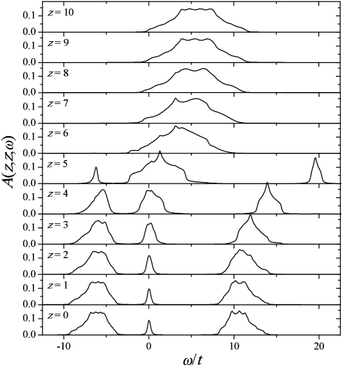
Dealing simultaneously with strong correlations and spatial inhomogeneity is a theoretical challenge. For this purpose, we generalized the dynamical mean field theory (DMFT) [5] to a multilayer geometry [3, 6], and solved the self-consistency equations with a Hartree approximation for the long-range part of the Coulomb interactions. Figure 1 shows a numerical result for the spatially-resolved spectral function of electrons, for a model Mott-insulator/band-insulator heterostructure [3]. Layers at and at correspond to a Mott-insulating region and band-insulating regions, respectively, and the layer at is the interface. At layers , the spectral function is essentially identical to that of a bulk band-insulator. Approaching the Mott-insulating region by reducing , the spectral function evolves fairly continuously. Eventually, the conduction band turns into a sharp quasiparticle band at the Fermi level, dominating the spectral weight at the interface layer . The existence of finite spectral weight at the Fermi level indicates the metallic property of the heterostructure. Penetrating into the Mott-insulating region , the quasiparticle bands loses its weight exponentially. These behaviors contrast with a simple band-bending picture for interfaces between two band insulators with a finite band offset.
The metallic behavior of such Mott-insulator/band-insulator heterostructures was actually reported experimentally in early work by Ohtomo et al. [1]. Furthermore, recent photoemission experiments on LaTiO3/SrTiO3 superlattices have confirmed the appearance of a quasiparticle band at the Fermi level, in agreement with the theoretical prediction [7].
The essential physics controlling the properties described above is the charge transfer between the two insulators. This creates intermediate filling regions, in between the fillings of the two insulators, which are responsible for the metallic behavior of the heterostructure. Therefore, even if the on-site interaction is strong enough to produce a bulk Mott insulator, metallic behavior survives at the interface. More realistic model calculations including orbital degeneracy and electron-lattice couplings further predicted interesting spin and orbital orderings that are different from bulk materials [3]. Electronic reconstruction, which is the appearance of new electronic phases that are different from the bulk electronic phases, at interfaces of correlated electron systems is a quite general phenomenon. Interesting novel electronic phases may result at the interface of properly chosen oxides. We will discuss such interface reconstructions in other models in the following sections.
3 Interfaces of manganites and cuprates
The simple setup and results of the previous section show that the transfer of charge between complex oxides should be a very general phenomenon. In this section, recent theoretical efforts in this context carried out by Yunoki et al. [4] are briefly reviewed (for more details the reader should consult the original publication). The main result of Ref. [4] was the prediction that a transfer of charge could occur from a manganite to the upper Hubbard band of some undoped cuprates (high-Tc parent insulators). Since electronic doping of some Cu oxides has led to superconductivity, potentially the manganite-cuprate multilayers discussed in [4] could also become superconducting.
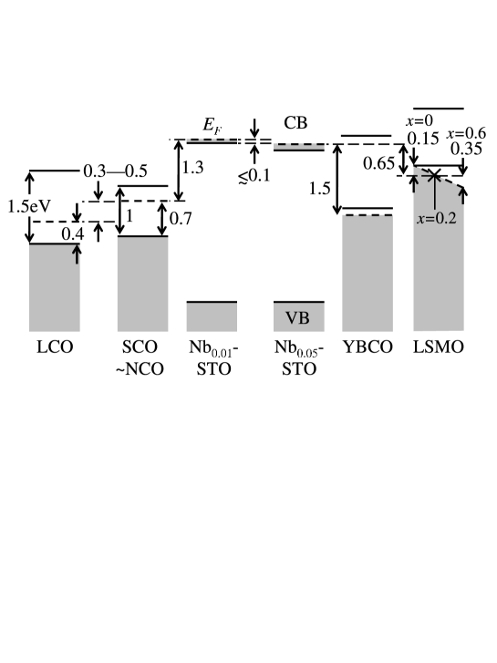
One of the main results of [4] is the discussion of a band alignment study of several oxides, which is illustrated in Fig. 2. Using experimental information, such as the work functions of oxides, the relative positions of the Mott gaps and the chemical potentials were (crudely) predicted. This plot suggests that the mixture of a manganite, such as La1-xSrxMnO3 (LSMO), and a doped superconducting cuprate, such as YBa2Cu3Oy (YBCO), should lead to the transfer of charge from LSMO to YBCO. This is in agreement with recent experimental results [8], giving confidence to the qualitative validity of the analysis. Moreover, new predictions can be made. For instance, mixing LaMnO3 (LMO) with Sm2CuO4 (SCO) should lead to the transfer of charge from LMO to the upper band of SMO, and probably to an electron-doped superconductor, as already mentioned. While more details about this particular case can be found in [4], here the main issue to remark is that by the procedure outlined in this section and [4], it is possible to make qualitative predictions for the direction of charge transfer at interfaces. This is of fundamental importance for the guidance of experimental efforts, since the number of combinations of oxides is enormous and theory must predict which of those combinations are potentially the most attractive for the fabrication of superlattices.
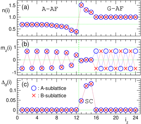
The intuitive picture based on the work functions, and the possible development of superconductivity in some cuprates via a proximity with the manganites, was further substantiated in [4] by actual numerical calculations. For example, Fig. 3 illustrates the results of a simple mean-field approximation. The upper panel shows the electronic density vs. position along the chain, for the case of an interface between an A-type AF state (simulating an undoped manganite) and a G-type AF state (simulating an undoped cuprate), after a Poisson equation iterative procedure is carried out. Details can be found in [4]. The middle panel illustrates the magnetic properties. The spin arrangement away from the interface is either A or G, as expected by construction. However, near the interface on the G-AF side (which simulates the undoped cuprate) an accumulation of electronic charge takes place due to the different chemical potentials of the two materials. This region is electron doped, reducing drastically the spin G-type AF tendencies. Concomitant with this reduction of antiferromagnetism, the lower panel shows the expected development of superconductivity. Thus, the theoretical calculations are in agreement with the simple picture based on the work functions. However, note that more sophisticated calculations, beyond the mean-field approximation, are needed to fully confirm these tendencies.

The possibility of generating an electron doped superconductor via charge transfer from other oxides may help in unveiling the true phase diagram of the high temperature superconductors. According to phenomenological calculations by Alvarez et al. [10], in the absence of quenched disorder (clean limit) the phase diagram of cuprates should have either a first-order transition separating the competing states or a region of local coexistence of both orders (actually, stripes are a third more exotic possibility, see [10]). None corresponds to the true (experimental) phase diagram of LSCO. The clean-limit proposed and actual experimentally observed phase diagrams are in Fig. 4. The key idea of [10] was the observation that the LSCO true phase diagram can be obtained from the clean limit phase diagram by merely adding quenched disorder. This opens a window in the phase diagram between the competing phases and induces an intermediate glassy state. If this observation is correct, then quenched disorder fundamentally affects the cuprate’s phase diagrams. Then, the possibility of doping Cu-oxide parent insulators via charge transfer in multilayers becomes a possible path to reveal the real clean-limit phase diagrams of the cuprates, which at present may be much distorted by the chemical doping procedure.
4 Superlattices of insulating materials can lead to a metal
Besides containing a brief review of recent work on interfaces of correlated electrons, this manuscript also includes new results that are described in this section. The goal here is to illustrate, with a simple example, how an array (multilayer) of thin layers (thin meaning just a few lattice spacings in width) can have properties drastically different from those of the bulk constituents. In particular, the cases of the Hubbard and DE models will be investigated. In both examples, the “building blocks”, namely the isolated layers, are insulating. However, it will be shown that the ensemble becomes metallic due to transfer of charge.
4.1 Superlattices in the Hubbard model
In this subsection, the results for a superlattice described by the well-known Hubbard model are presented. The heterostructure studied here is formed by alternating layers of two different materials, labeled A and B, which are chosen to be insulating and chemically homogeneous. In the simple Hubbard electronic Hamiltonian, each material can be parametrized by selecting its electronic density, which in the bulk locally matches the charge of the positive ions for an homogeneous system. Let us assume that only one band is relevant to determine the properties of the material under study: then the system can be described by the (single-orbital) Hubbard model defined by
| (1) |
where is the creation operator for an electron with spin projection at site , is the hopping integral between neighboring sites, and denotes nearest neighbors; gives the number of electrons at site , is the on-site Coulomb repulsion, and is the electronic potential (discussed in more detail later) that will take into account effects related to the charge redistribution. is the chemical potential, while and are site potentials. Finally, to simplify the numerical task, without altering the qualitative aspects of the conclusions, a one-dimensional arrangement will be studied. The simplicity of the results described below lead us to believe that the conclusions are valid in higher dimensions as well.
Note that has contributions coming from both the ionic and electronic charges. While the ionic part can be easily calculated, the dependence on the electronic densities makes a complicated operator. In the continuum limit, should be determined by the Poisson equation. Therefore, we can use an iterative procedure to calculate the ground state properties of the Hamiltonian (1) [11]. For a given iteration it, we assume that we have a guess for the electronic charge distribution that is used to calculate by solving the discretized Poisson equation:
| (2) |
where , is the dielectric constant, is the charge of the electron , and is the lattice constant. The right-hand-side of the equation is a lattice discretized version of the second derivative operator. The ground state of the Hamiltonian (1), , is calculated via the DMRG algorithm [12] using . The value for the next iteration is calculated as , where and . The procedure is repeated until the set converges.
To calculate the ground state we typically keep 200 states per DMRG block. We perform enough number of DMRG sweeps between two consecutive solutions of the Poisson equation to verify that each is converged for the used. In practice, typically and . We have found empirically that the iterative procedure is particularly difficult to converge for , if .
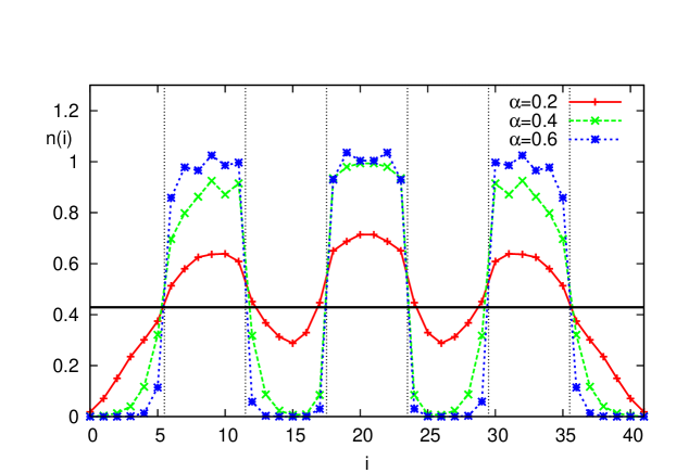
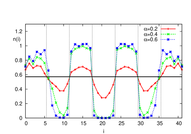
Typical results are shown in Fig. 5 where the charge density profile along the chain, parametric with the reciprocal value of the dielectric constant , is given for the case of two insulating materials with =1 and =0, and in the realistic limit where is much larger than (namely, when a robust Hubbard gap develops at half-filling; is an atomic coupling in the range of a few eVs, while is just a fraction of eV). From the figure, it can be easily observed that the long-range Coulomb interaction, considered via the Poisson equation, alters qualitatively the charge profile from a highly inhomogeneous insulating state for large (with electrons following the positive charge density of the bulk materials) to a nearly homogeneous metallic state for small . This last observation is the main result of this section: the fact that the multilayer system is made out of thin layers allows the electronic charge to be redistributed all along the heterostructure. From previous investigations of the Hubbard model, it is known that this model with electronic density 0.5 is metallic. Thus, by mixing insulators, a metal emerges in the multilayer geometry for sufficiently thin layers, a remarkable result.
4.2 Superlattices in the Double Exchange model
The previous Hubbard model results could be used for interfaces involving a Mott insulator and a band insulator. However, if one of the building blocks is a manganite, then the DE model should be employed. This DE model takes into account that the electrons that form the bands close to the Fermi level are in partially filled -orbitals. The degeneracy of the -orbitals is usually removed by the crystal field created by the underlying crystalline structure. This results in the appearance of a gap between the different representations of the -orbitals in the symmetry group of the ionic lattice, for example between the and orbitals in the case of the perovskite tetragonal structure. The filled sub-band can be described by a localized spin. In the case of interest here (LaMnO3 (LMO) and SrMnO3 (SMO)), the sub-band is higher in energy than the sub-band, which is filled and it is represented by a localized -spin (usually assumed classical for simplicity). Then, a manganite system can be described by the DE Hamiltonian [9]:
| (3) | |||||
where now creates an -electron at site with spin projection . For simplicity, here only one band in the manifold is used, a widely used approximation. is the hopping integral between neighboring sites for the electrons in this sub-band; is the Hund coupling between the electrons in the sub-band; and is the antiferromagnetic exchange interaction between neighboring localized spins, which takes into account the virtual hoppings in the sub-band. are Pauli matrices, and is a classical localized spin at site i () representing the spins. More details about this model and the physics of manganites in general can be found in [9].
The considerations related to the long-range portion of the electrostatic potential used in the previous subsection remain valid here as well, and a similar iterative procedure is also used. The difference is that the ground state of the Hamiltonian (3) is solved by the numerical Monte Carlo method, instead of the DMRG technique. The Hamiltonian is separated in spin and electronic components. The electronic portion is treated exactly via library subroutines. The localized spins are treated in the classical approximation using a Monte Carlo algorithm [9].
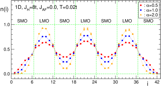
Regarding the distribution of electronic charge, the results are qualitatively similar to those in the case of the Hubbard model. A typical case is shown in Fig. 7 at low temperature. Once again, as is reduced the charge spreads, and its value is far from the nominal 1 and 0 of the building blocks. Clarifications are here in order: (1) The coupling =8 is realistic, as widely discussed in previous literature [9]. In fact, is estimated to be a few eV’s, while the hopping is always just a fraction of eV. Note that is a local on-site ferromagnetic interaction, and it is not the actual parameter directly regulating the strength of the critical temperature. The latter arises from an effective double-exchange coupling between nearest neighbors spins. (2) The limit =0 is chosen for simplicity. It is already well-known [9] that at =0, and with one -electron per site in the one-orbital model, the ground state is antiferromagnetic. Then, LMO is properly described. Regarding SMO, a better description would have needed 0, to represent the antiferromagnetism present in the limit of zero carriers. However, this approximation does not at all affect the conclusions (see below) of our effort.
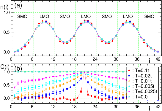
For the case of the DE model, the magnetic properties are more interesting than for the Hubbard model. The reason is that together with the metallicity induced by charge transfer in a multilayer structure, the magnetic properties change from antiferromagnetic (for the bulk components LMO and SMO) to ferromagnetic (in the multilayer). This is illustrated in Fig. 8, for =1. The upper panel shows the charge density, which is not changing much in the range of temperatures investigated. However, the lower panel, with the spin-spin correlations, indicates clearly the development of ferromagnetism upon cooling. The reason is simple. The electronic density is no longer 1 or 0, as in the LMO and SMO limiting cases, but at every site this density becomes an intermediate number between 1 and 0. This charge doping leads to ferromagnetic tendencies, since the well-known DE mechanism becomes active upon doping [9]. In fact, it is known from previous investigations that the tendencies toward ferromagnetism are the strongest at electronic density 0.5, and they survive in a wide range of dopings. From this perspective, the results are easy to understand: (1) the long-range Coulomb interaction spreads the charge, effectively doping LMO with holes and SMO with electrons; (2) in hole or electron doped manganite antiferromagnets, the DE mechanism leads to ferromagnetism. However, there is an important difference between multilayers and bulk compounds: the chemical doping procedure usually employed to dope oxides, for instance substituting La by Ca, is now replaced by a mere spreading of the charge in the vicinity of the interface. Then, the influence of quenched disorder is reduced by this procedure, as already discussed in the case of superconductors in previous sections.
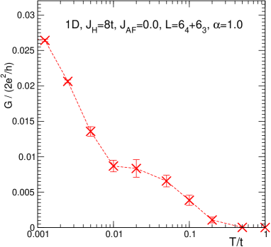
The ferromagnetism goes together with metallicity, as shown in Fig. 9 where the conductance is given as a function of temperature. Similarly as it occurs in bulk DE models, the appearance of ferromagnetism also leads to a substantial increase in the conductance. The conductance increase with reducing temperature signals the existence of a metal in the multilayer system that is made out of antiferromagnetic insulators, which is a conceptually interesting result. Novel properties arise in the multilayer structure as a whole that are not present in the individual materials that form the multilayer.
5 Conclusions
In this manuscript, recent investigations by the authors in the area of interfaces of complex oxides, using modeling techniques and numerical simulations, were briefly reviewed. In addition, new results corresponding to multilayers of insulating antiferromagnets (in a 1D arrangement for simplicity) were also presented. The spreading of charge between the two materials involved in the multilayer is sufficiently strong to generate a metallic state, which in the case of the manganites is ferromagnetic due to the DE effect. These simple examples illustrate the potential of working with oxide multilayers: they provide us with a novel procedure to tune properties of materials by adjusting the width and the nature of the components themselves. The number of combinations is huge and this field of research is in its early stages. The experimental effort clearly needs theoretical guidance to establish which are the most interesting combinations of oxides to investigate. This new “playground” for correlated electrons surely will provide several surprises in the near future, which not only may influence on fundamental research in complex oxides by generating new interfacial phases, but may also be of potential relevance in devices in the growing field of oxide electronics.
References
References
- [1] A. Ohtomo, D. A. Muller, J. L. Grazul, and H. Y. Hwang, Nature 419, 378 (2002). See also A. Ohtomo and H. Y. Hwang, Nature 427, 423 (2004); N. Nakagawa, H. Y. Hwang, and D. A. Muller, Nature Materials 5, 204 (2006); S. Thiel, G. Hammerl, A. Schmehl, C. W. Schneider, and J. Mannhart, Science 313, 1942 (2006).
- [2] E. Dagotto, Science 309, 257 (2005), and references therein.
- [3] S. Okamoto and A. Millis, Nature 428, 630 (2004); S. Okamoto and A. J. Millis, Phys. Rev. B 70, 075101 (2004); S. Okamoto and A. J. Millis, Phys. Rev. B 70, 241104(R) (2004); S. Okamoto, A. J. Millis, and N. A. Spaldin, Phys. Rev. Lett. 97, 056802 (2006).
- [4] S. Yunoki, A. Moreo, E. Dagotto, S. Okamoto, S. S. Kancharla, and A. Fujimori, Phys. Rev. B 76, 064532 (2007).
- [5] A. Georges, B. G. Kotliar, W. Krauth and M. J. Rozenberg, Rev. Mod. Phys., 68, 13 (1996).
- [6] M. Potthoff and W. Nolting, Phys. Rev. B 59, 2549; 60, 7834 (1999); S. Schwieger, M. Potthoff, and W. Nolting, Phys. Rev. B 67, 165408 (2003).
- [7] M. Takizawa, et al., Phys. Rev. Lett. 97, 057601 (2006).
- [8] J. Chakhalian, J. W. Freeland, H.-U. Habermeier, G. Cristiani, G. Khaliullin, M. van Veenendaal, and B. Keimer, Science 318, 1114 (2007). See also E. Dagotto, Science 318, 1076 (2007).
- [9] E. Dagotto, T. Hotta, and A. Moreo, Physics Reports 344, 1 (2001).
- [10] G. Alvarez, M. Mayr, A. Moreo, and E. Dagotto, Phys. Rev. B 71, 014514 (2005). See also M. Mayr, G. Alvarez, A. Moreo, and E. Dagotto, Phys. Rev. B 73, 014509 (2006).
- [11] T. Oka and N. Nagaosa, Phys. Rev. Lett. 95, 266403 (2005).
- [12] S. R. White, Phys. Rev. Lett. 69, 2863 (1992). S. R. White, Phys. Rev. B 48, 10345 (1993).
- [13] Additional results in 1D structures can be found in S. S. Kancharla and E. Dagotto, Phys. Rev. B 74, 195427 (2006).