Quasiparticle Trapping In Three Terminal Ferromagnetic Tunneling Devices
Abstract
Hybrid Superconductor/Ferromagnet structures have been investigated recently to address the interplay between ferromagnetism and superconductivity. They also open up new routes for the investigation of out of equilibrium superconductivity. Here, we show how it is possible for out of equilibrium excitations produced in a superconducting thin film (S) to be localized in a ferromagnetic trap (F). Specifically, a ferromagnetic nano-volume in good contact with S represents a potential well for the quasiparticles (QPs) at the gap edge. As the superconducting proximity effect is highly suppressed in F, QPs get efficiently trapped and they share their energy with the free electrons in the trap. The electronic temperature in the trap can be increased by up to from the bath temperature at mK as measured by tunneling spectroscopy using a second junction.
pacs:
PACS numbers: 74.45.+c, 75.50.+rI Introduction
Superconductor/Ferromagnet (S/F) hybrid nanostructures open up new routes to study the interplay between superconductivity and ferromagnetism. The main advantage is that unlike in bulk materials, in nanostructures despite the fact that superconducting gap () and ferromagnetic exchange energy () are not comparable, superconductivity and ferromagnetism do not exclude one another. This is because these two antagonistic ground states influence each other only near the interface. Nonequilibrium superconductivity in such structures is a new topic. After a superconductor absorbs energy, excess quasiparticles (QPs) with non- thermal distribution are created. Their energy relaxation occurs via two different mechanisms: electron-electron (-) and electron-phonon (-) interactions. The timescale for energy relaxation depends on the respective scattering rates ( and ), both of them rapidly increasing with the excitation energy. ref1 The Fermi-Dirac energy distribution of QPs is reached on a timescale larger than , while in the limit of strong - relaxation, QP temperature becomes equal to the lattice temperature. ref2
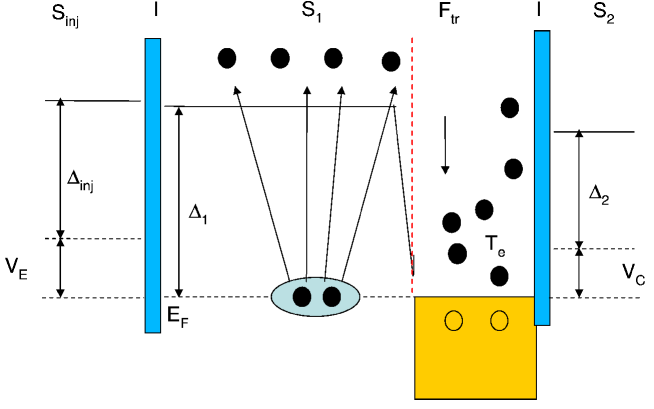
To be more specific, when a superconductor absorbs energy , within a few picoseconds it goes into a nonequilibrium state, consisting of broken Cooper pairs and high energy phonons with energies close to the cutoff Debye energy. ref3 In a fast nanosecond cascade, energy is distributed over an increasing number of QPs and phonons, decaying until it reaches the gap edge. Both excess QPs and phonons have limited lifetimes. Quasiparticles may recombine into Cooper pairs, diffuse, get scattered by impurities, or get trapped and frozen, while phonons can get scattered or escape into the substrate. The characteristic timescale of QP recombination into Cooper pairs goes from the ns until a few depending on material parameters. ref1 If the superconductor is coupled to another superconductor via a tunnel junction, excess carriers can tunnel through the barrier. At low temperatures (, where is the superconducting critical temperature), recombination time is longer than the tunneling time, ref2 ; ref4 therefore majority of QPs can tunnel, creating current through a tunnel junction. As the magnitude of current from a detector tunnel junction is inversely proportional to the volume of the source superconductor , ref5 in order to enhance the readout signal, Booth proposed the idea of QP trapping in a small volume layer that can be either a superconductor with a smaller gap than that of or a normal metal. ref6 We show a typical quasiparticle trapping device on Fig.1. The current is injected into the device via a tunnel junction from superconductor , and detected through another tunnel junction with superconducting electrode .
We have considered a ferromagnetic trap () and investigated the energy confinement produced by downconversion of QPs coming from into . As no gap is induced in by proximity effect, a ferromagnetic trap allows QPs to relax their energy in a volume much smaller than that of a normal trap, increasing the QP accumulation and hence the local energy density. We have fabricated three terminal Josephson tunnel devices of different sizes and geometries. QPs are injected into from a tunnel junction, they relax at the gap edge and then they are trapped in where through - interaction they locally raise the electron temperature . The temperature of these nonequilibrium carriers in is probed by tunneling spectroscopy, measuring the current-voltage characteristics of a second tunnel junction connecting layer and . We show that in mesoscopic devices, ferromagnetic trapping is efficient in raising the local electronic temperature from the bath temperature of mK up to mK.
The paper is organized as follows. In section II, we describe the principle of quasiparticle trapping. In section III we present the principle of operation of three terminal tunnel junction devices using a ferromagnetic trapping layer. In section IV we describe our three terminal macroscopic device consisting of two stacked tunnel junctions and present its characterization in terms of conductance variation with QP injection. In section V we present our planar mesoscopic three terminal device, consisting of two tunnel junctions connected with a sub-micrometric S/F bilayer. We also measure conductance as a function of steady-state current injection. In section VI we discuss the results and trap heating in terms of a simple non equilibrium model.
II Principle of Quasiparticle Trapping
As first proposed by Booth, ref6 trapping of excitations in a small junction has been considered as an alternative to fabrication of large area detectors, whose high capacitance limits both the frequency response and the energy resolution. Excess QPs created by either Cooper pair breaking or injection (see Fig.1) diffuse from to the trap, where they relax their energy and are confined. From this intuitive physical picture, it is clear that the trap layer has two crucial functions: it prevents back diffusion of QPs, and with its smaller volume it increases the magnitude of the readout signal, since the density of out of equilibrium quasiparticles , for a fixed energy, is proportional to the inverse of the trap volume , where is the injected current, the trap volume and the time spent in the trap before relaxation. However, if the volume is too small, phase coherence is preserved in the trap resulting in a superconducting proximity effect. The induced gap in the density of states in the trap reduces the number of QPs available to relax the energy, and hence heating.
The choice of materials for the Superconductor/Trap () bilayer is, therefore, crucial for correct operation. Firstly, will be chosen for long QP lifetimes and high QP diffusion velocities to ensure that QPs reach the trap before recombination. Secondly, it is important that interfaces between and are clean, to facilitate the diffusion. Thirdly and most importantly, we need a small superconducting proximity effect in the trap layer. We should make a trap layer sufficiently thin in order to get a high density of nonequilibrium QPs, but not too thin as it should remain in the normal state in contact with through a highly transparent interface. Despite considerable efforts in several laboratories, the right compromise between these constraints is still under investigation.
N.E. Booth et al. ref7 and Ullom et al. ref8 ; ref9 have extensively studied normal trap efficiency, defined as the ratio between detected and injected power, in a system consisting of an Al superconducting reservoir , and Ag as the normal metal trap. They used a three terminal device following the diagram shown in Fig.1. Tunneling through a detector junction determines the dwell time and the speed of the detector, both of the order of . Ullom et al. described the QP diffusion in terms of a renormalized, energy dependent diffusion coefficient , where is the QP group velocity that drops to zero at the gap edge, is the superconducting gap, the Fermi velocity, the energy measured from the Fermi level and is the bulk diffusion coefficient. They have measured at mK up to efficiency. Because of the large device size (), QP losses were mainly due to recombination. In another series of experiments with excitations produced in In crystals by a low power pulsed laser, Goldie et al. ref5 studied trapping into Al and Cu thin films ( to nm) deposited on In always finding a minigap induced in the Cu by the proximity effect. Pepe et al. ref10 reported nonequilibrium measurements under steady state current injection in a stacked double superconducting tunnel junction device with middle electrode consisting of an Nb/Al bilayer where the Nb is the superconductor and the Al the trap. They found that the nm thick Al trap layer was strongly proximised by a nm thick Nb film. They also found that the proximity effect is reduced as a function of the injection current, without any appreciable modification of the interface transparency. Zehnder ref11 has studied how external energy is stored for different junction materials. He found losses mainly due to the presence of the sub-gap phonons in the trapping layer. Efficiency scales inversely with the mean free path of the material. He also pointed out that for large area () Nb/Al structures the density of states is spatially dependent. As a consequence, the trapping process becomes local, and hence both QP lifetime and trapping rate.
In the present work we propose a new direction, the reduction of the trap volume using a ferromagnet . The superconducting proximity effect extends in the ferromagnet over a coherence length given by that varies between and nm and is almost times smaller than the coherence length of a normal metal with the same diffusion constant, . This extremely reduced proximity effect provides a more efficient energy localization. So, a hybrid, mesoscopic S/F heterostructure seems to be a unique candidate to obtain the smallest, not proximised trap.
III Three terminal device operation
Here we describe the working principle of our realization of the ferromagnetic quasiparticle trapping transistor (FQTT) based on the description proposed by Booth et al. ref13 The ferromagnet is a alloy. ref14 We choose this alloy because: . the small ferromagnetic coherence length (nm); . Pd has an almost filled band, and the large density of states at the Fermi level provides more conduction electrons available in the trap; . electronic specific heat is high ( orders of magnitude higher than pure Copper, for example), ref15 which means that energy is ”stored” in the electron gas, with substantially longer - relaxation time. It is worthwhile to point out that long - relaxation time leads to a small bandwidth.
The principle of operation of our devices can be obtained considering a simple static balance of power flow into the layer. To do this, we borrow the common semiconductor transistor terminology. We call / bilayer the base, the emitter, and the collector. Current is passed through the first junction emitting quasiparticles. The net power injected into is , where is the average injected QP energy, which depends on the voltage across the tunnel junction. A part of the incoming power is lost via thermal interaction with the phonon lattice, . It can be calculated using the so called -T nonequilibrium model, ref16 in which different temperatures and and specific heats and are assigned to the electron and phonon systems, which are considered to be decoupled at low temperatures. The energy transfer rate from electrons to phonons in the / bilayer is given by , where is a material-related parameter (varying in the range of - and is the volume of the trap. Here we explicitly assume that the phonon system is at the external bath temperature. This hypothesis, as we shall see later, depends on the details of the film geometry and coupling to the substrate, via the Kapitza interface conductance.ref17 Injected power is also evacuated via the detector tunnel junction, by cooling through tunneling. This happens when a NIS junction is biased at a voltage lower than the superconducting gap, so that only the hot electrons from the tail of the Fermi distribution can tunnel from the normal to the superconducting electrode. Self cooling, by removing high energy electrons, causes a progressive transfer of energy out of the normal film.ref18 The cooling power of the junction when polarized at the gap edge is given by , ref19 where is the normal state resistance of the junction. In the experiments described below the cooling power can be neglected and hence as we shall see below all the injected energy is lost by phonon interactions:
which yields:
| (1) |
If high energy QPs are injected with ), the most efficient mechanism for energy redistribution within the electron subsystem becomes the emission of Debye phonons. The mean free path of these phonons is very small, and they efficiently excite additional electrons and break Cooper pairs in the reservoir. Nonequilibrium vibrations isotropically propagate through the whole system, mixing and coupling the electronic and phononic subsystems. As a result, delocalized heating takes place and energy confinement is no longer possible. Therefore it is important to work at energies near the gap edge in order to avoid phonon losses (which multiply with the increase of the injection energy) and transfer the injected energy solely to the electronic system.
IV Stack junction device
We have fabricated two kinds of three terminal structures with different geometries and sizes. In both we chose Al as superconductor for its long recombination timeref20 . ref1
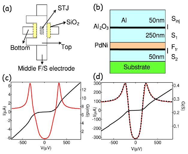
The first macroscopic device that we shall present consists of two stacked junctions (area of ). We put electric contacts so that we can bias each junction independently. The stacked structures used for the experiment described in the following are sketched in Fig. 2 in a top (a) and cross-section (b) view. Four stacked junctions are fabricated simultaneously on a single Si wafer, with common bottom electrode. All layers were fabricated in situ using thin film evaporation, in an ultra high vacuum system with a base pressure of . The fabrication procedure is as follows. On a Si substrate we evaporated through a metallic mask the first nm-thick Al layer. This layer will be the bottom electrode of the device, common to all the junctions of the sample. Then we oxidize the Al layer by plasma at about pressure. The junction area is defined by evaporating nm-thick orthogonal striplines of SiO in order to define a square of . Then, a layer of PdNi ( Ni) is evaporated as ferromagnetic trap . We have varied the thickness (, , nm) of the (PdNi) layer. The trap volume is for nm of PdNi. Then we evaporated nm of Al as superconducting layer . We repeated the oxidation and SiO deposition in order to make a second tunnel barrier, and finally evaporated nm of Al as layer .
The junctions quality was systematically checked by measuring the current-voltage characteristics and the tunnel conductance with the standard ac modulation technique. All the measurements were carried out at mK in a cryostat. In Fig.2 (c) and (d) are shown two typical I-V curves and tunnel conductance spectra of an (SIS) junction and an - (SIF) junction, respectively. Quasiparticle current is suppressed below , i.e. twice the Al gap for the upper SIS junction, while for the bottom SIF junction we measure a voltage gap of showing no proximity effect in F. The tunneling spectrum of the bottom junction is well fitted by the conventional BCS density of states (dashed line), instead the upper junction shows that the Al on the PdNi has not fully recovered its BCS density of states and states in the gap are partially occupied. Normal resistances are for SIS and for SIF junction. The critical temperature of the PdNi/Al bilayer is .
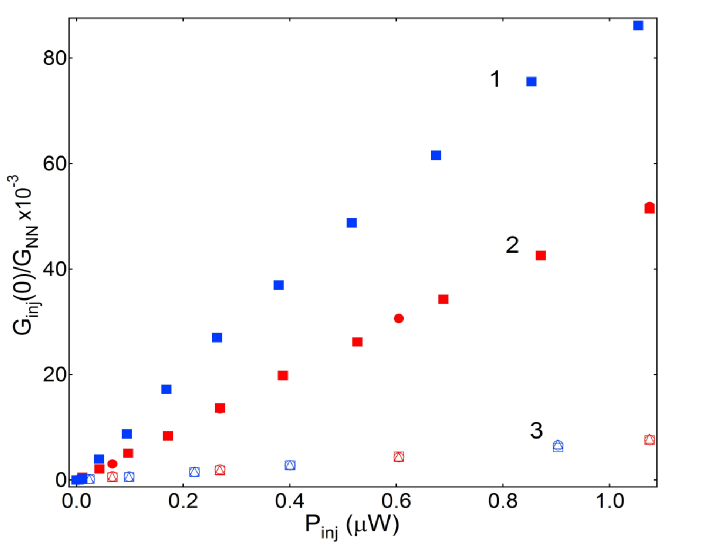
We measured the dynamical conductances of the bottom junction under injection of current between and from the top junction. We did not observe any enhancement in the detection spectra at energies close to the gap, while at energies or even times larger, zero bias conductance increases linearly in power (variations of about of the normal state conductance are measured) due to hot electrons. We have also reversed the roles of the junctions. The injected power is of the order of in both configurations. As shown in Fig. 3, marker groups (1) and (2) refer to the injection and detection in the same stack. Markers (1) corresponds to injection from the SIF and detection at the SIS and markers (2) to the inverse. As , phonon emission drives the relaxation process, we measure twice higher signal when injecting from the SIF (1) rather than the SIS (2) junction because of the double convolution by the QP density of states of the two superconducting electrodes.
Markers (3) refer to injection and detection between junctions of different stacks. All marker groups (3) are practically superimposed, regardless of the direction of injection. No differences are observed in the detector as a function of the distance from the injector. Therefore even though energy is not localized in , the lack of accumulation is not due to the out diffusion of the QPs away from the detector junction area into the surroundings. Indeed, from the recombination time ref1 which sets the upper limit for QP diffusion, we found diffusion length , which is small compared to the dimensions of our device. Moreover, we did not register any difference between the injection from the top/bottom junction of the stack and detection with the bottom junction of the neighboring stack. This implies, as the bottom electrode is geometrically common to all the junctions of the sample, that the tiny raise in the tunneling conductance (i.e. markers (3)) is mainly due to a small rise in the substrate temperature (we also did not measure any thermal gradient between neighboring junctions). Let us consider the power balance and the dynamics of excitations in the PdNi trap. We calculate specific heat of electron and phonon subsystems: , where the linear contribution is due to electrons and cubic to phonons. From the molar volume of the trap () we have: and and hence: while at mK. We found that the electron-phonon conductance () at mK is and the electron-phonon scattering time () is . Once thermal excitation is transferred to the lattice, energy can flow by thermal conductance to the substrate. This transfer is limited by thermal boundary resistance, the Kapitza resistance, . Typically, . Thus the effective conductance will be:
There are two boundaries to consider: PdNi to Al bottom electrode, and bottom electrode to substrate. We neglect the boundary between the surface oxide on the substrate and the single crystal Si wafer. So, taking as area a larger value of about and considering the series of two interfaces, we obtain , which implies about a factor larger than . The phonon temperature is uniform on the sample. This implies that our substrate has very good coupling to the / bilayer.
We now discuss why the ferromagnetic trap is not working properly. The trap works at the gap edge and, in our case, at that energy the flow of injected QPs is too small. In fact, the density of out of equilibrium QPs in the trap must be higher than that in the thermal equilibrium, , for the trap to be effective. This condition imposes a lower bound on the lifetime of the out of equilibrium excitations in the trap as and , where is the injected current (typically of about at the gap edge with our resistance values), is the trap volume, and is the density of electron states at the Fermi level. We estimated that of about is required to accumulate excitations with a number higher than . This time is much larger than any characteristic timescale and in particular , thus excitations out of equilibrium created by injection are practically lost via phonons. The trap is inefficient and the conductance at zero bias independent of injection at energy comparable with the Al gap edge.
The first obvious solution is to increase the injected current density.
V Mesoscopic planar device
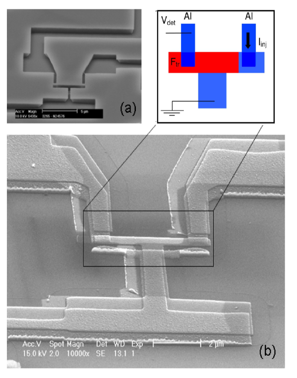
We fabricate a new type of mesoscopic planar device to get smaller volumes and higher trap efficiency. This type of device is represented in the photo of Fig. 4(b). Two sub-micrometric tunnel junctions are separated by middle, double layered Al-PdNi common electrode, the trap.
The fabrication is as follows. We used a trilayer suspended mask consisting of nm of polymer polyether sulphone (PES), nm layer, and nm PMMA layer. The mask is patterned by electron beam lithography and the pattern transferred to the layer by plasma reactive ion etching at a pressure of mbar for about seconds. Then the PES is etched with plasma at a pressure of mbar for minutes, which gives an undercut of about nm. The SEM photo of the mask is shown on Fig. 4(a). Our samples were fabricated by angle evaporation in an ultrahigh vacuum system with a base pressure of about . First nm of Al were evaporated. The Al was oxidized in pure flux at a pressure of . Then a nm-thick Al layer was evaporated, followed by a nm-thick PdNi layer. Four devices are fabricated on the same wafer. The schematic of the device is shown in Fig. 4(c). The first, right-side junction is separated by another junction of the same area by a long Al layer which is partially () recovered by a thinner ferromagnetic PdNi layer. The magnetic layer is used to suppress superconductivity by inverse proximity effect and it defines the trap. Trap volume is i.e. about times smaller than the trap used in the stacks.
Note that the F layer plays a slightly different role in this device, since the QPs coming from the Al superconducting electrode tunnel into the Al and then diffuse lateraly into the PdNi/Al bilayer made up of the same Al. As the reservoir and the trap are made of the same material, matching of the Fermi velocities is optimal and so is the QP transmission. Furthermore, in this planar structure we deal with lateral trapping, which allows to avoid back tunneling of QPs, responsible for reduced cooling power. ref21
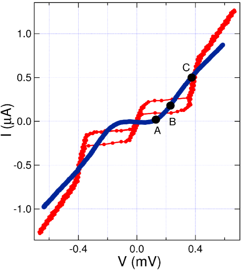
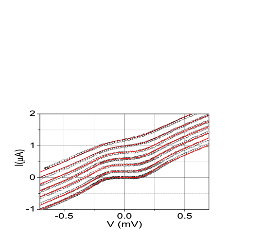
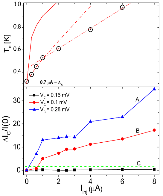
In Fig. 5, the I-V curves of the (SIS) and the (SI/SF) junctions are shown. The normal state resistances are about and respectively. Junction resistances higher than those measured in the stacks result in reduced injected power (now ranging from pW to nW). The gap voltages are and , as expected for inverse proximity effect. Moreover, the I-V curve of the SI/SF junction is well fitted by integrating the BCS density of states with an Al energy gap of and a base temperature of mK (see Fig. 6). The SIS junction is hysteretic with critical current of nA and retrapping current of nA. The finite resistance at zero bias is due to the bilayer trap resistance in series with the junction. The principle of the experiment is the same as that described above. Out of equilibrium excitations are collected in the SF trap rising the electron temperature , which is measured by tunneling spectroscopy. Different conductance spectra were measured while increasing the DC injection current through the SIS junction from to , as shown in Fig. 6. We obtain from the BCS fits also shown in Fig. 6 as red curves. The electron temperature as a function of the injected current is plotted in Fig. 7, top panel, markers. The temperature rises rapidly up to K, and then reaches K more slowly, resulting in two different slopes. Unlike stack junctions, the temperature in the planar trap increases significantly for the injection of QPs with energy comparable with the superconducting gap energy. Furthermore, the crossover between these two regimes is set by a voltage bias corresponding to the gap edge as expected because trapping, and hence energy localization, are more efficient below the gap edge. As injection energy increases ( times more for ), out of equilibrium phonons are emitted before the QPs reach the trap. High energy relaxation occurs mainly by phonons and phonon losses reduce the energy localized in the trap, resulting in a smaller temperature increase.
VI Trap heating
For quasiparticle energy relaxation in the trap is possible because, firstly, at K the trap size is larger than , secondly, the electron-phonon scattering time is much longer than ns and thirdly, the trap is located at a distance of about a micrometer from the SIS junction. This distance is much smaller than the recombination length as estimated above. An estimation of the electron-phonon scattering time from the electron-phonon conductance and the specific heat gives . The effective surface trap area evaluated from the SEM image is about and it gives Kapitza conductance from the phonon bath to the substrate. As , the phonons in the device are thermalized at the phonon base temperature. The bandwidth of the device is limited by the smallest between thermal tunneling and electron-phonon time. ref13 In Table I are summarized all the relevant physical parameters that determine QP trapping, for both stacks and mesoscopic devices investigated here.
In Fig. 7 (top panel, full line) we report the temperature increase as estimated from Eq. (1) considering negligible cooling by tunneling. (An estimate gives about pW, a factor hundred smaller than the injected power.) The actual temperature increase is lower than that obtained considering only cooling by phonons (solid line). Instead, we found good agreement by introducing a QP thermal loss (dotted-dashed line), , where is the thermal conductivity of the Al leads whose normal state resistance is .
Now let us discuss the current gain. The excess current of the SI/FS junction normalized to the value for zero injected current, , for three different voltage bias values, is shown in Fig. 7, bottom panel. When biasing well above the gap voltage (curve C on Fig. 7 corresponding to point C on Fig. 5, ), no excess current is measured. This range corresponds to the high energy tails of the QP DOS and it is almost independent of injection. When we approach the gap voltage we measure more pronounced variations of the collected current. When we polarize the detector junction at (i.e. below the gap voltage, point A on Fig. 6) we measure an increase of the tunnel current up to times. As expected, it is at energies near the gap that the increase of current is maximum: at , point B on Fig. 6, the collected current is up to times . It is important to note that the trapping mechanism not only controls the number of out of equilibrium QPs, but also the direction of the energy flow.
If we reverse the roles of the junctions, injecting from the SI/SF and detecting at the SIS, we do not register any increase of output current. All the current values detected in the reversed configuration fall below the dashed line in Fig. 7, low panel. Therefore, the ferromagnetic trap introduces a strong asymmetry in the device. Good isolation is very interesting for applications. However the amplification parameter as defined by Booth, ref13 , where and are, respectively, the collected and injected currents, normalized to the current gap values , is for detection at constant normalized voltage . Higher amplification may be achieved at lower temperature and highly thermally isolated traps.
VII Conclusion
We have investigated a three terminal device consisting of two superconducting tunnel junctions coupled via an S/F bilayer. The ferromagnetic layer is used to localize and multiply QPs injected from the base junction. QP excess current is measured through the second detecting tunnel junction. We measured conductance spectra of the detecting junction as a function of the injected power for two types of structures fabricated with the same S/F materials: a stacked macroscopic and a planar mesoscopic device. We have found efficient trapping in the mesoscopic device, where it is possible to increase the local electronic temperature by up to of the base temperature. We have also found that input is well isolated from the output as a consequence of using the ferromagnetic trap, making the device attractive for transistor-like operation. However the gain at mK is .
Acknowledgements.
This work was partially done at the Quantum Physics Laboratory at the ESPCI and it was supported by the ESPCI and the ESF through the ”Pi-Shift” project. It has also been partially supported by MIUR under the Project PRIN 2006 ”Macroscopic Quantum Systems-Fundamental Aspects and Applications of Unconventional Josephson Structures. N. Booth, J. Lesueur, B. Leridon, B. Reulet, G. P. Pepe and A. Barone are gratefully acknowledged for several ideas and discussions. We also thank S. Collin for technical assistance and J. Y. Prieur for a critical reading of the manuscript.| Device | Macroscopic stacked | Mesoscopic planar |
| Trap volume [] | ||
| 200 | 0.02 | |
| 5 | 0.5 | |
| 2.2 | 0.01 | |
| 700 | 0.07 | |
| Injected power [nW] | 1000 | 1 |
References
- (1) S. B. Kaplan, C. C. Chi, D. N. Langenberg, J. J. Chang, S. Jafarey, and D. J. Scalapino, Phys. Rev. B 14, 4854 (1976).
- (2) R. Cristiano in Superconducting detectors (Proceedings of 5th SceNet School, Spain, 2004).
- (3) A. Zehnder, Phys. Rev. B 52, 12858 (1995).
- (4) Nonequilibrium Superconductivity, Phonons, and Kapitza Boundaries, edited by K. E. Gray (Plenum, New York, 1981).
- (5) D. J. Goldie, N. E. Booth, C. Patel and G. L. Salmon, Phys. Rev. Lett. 64, 954 (1990).
- (6) N. E. Booth, Appl. Phys. Lett. 50, 293 (1987).
- (7) J. N. Ullom, P. A. Fisher and M. Nahum, Nucl. Instr. and Meth. A 370, 98 (1996).
- (8) J. N. Ullom, P. A. Fisher and M. Nahum, Phys. Rev. B 58, 8225 (1998).
- (9) J. N. Ullom, P. A. Fisher and M. Nahum, Phys. Rev. B 61, 14839 (2000).
- (10) G. P. Pepe, G. Peluso, R. Scaldaferri, A. Barone, L. Parlato, R. Latempa, and A. A. Golubov, Phys. Rev. B 66, 174509 (2002).
- (11) A. Zehnder, Ph. Lerch, S. P. Zhao, T. Nussbaumer, E. C. Kirk and H. R. Ott, Phys. Rev. B 59, 8875 (1999).
- (12) S. E. Shafranjuk and I. P. Nevirkovets, IEEE Trans. on Appl. Sup. 15, 1051 (2005).
- (13) N. E. Booth, P. A. Fisher, M. Nahum and J. N. Ullom, Supercond. Sci. Technol. 12, 538 (1999).
- (14) A. W. Overhauser and A. I. Schindler, J. Appl. Phys. 28, 544 (1957).
- (15) G. Chouteau, R. Fourneaux, R. Tournier and P. Lederer, Phys. Rev. Lett. 21, 1082 (1968).
- (16) V. E. Gusev and O. B. Wrigth, Phys. Rev. B 57, 2878 (1998).
- (17) E. T. Swartz and R. O. Pohl, Rev. Mod. Phys. 61, 605 (1989).
- (18) F. Giazotto, T. T. Heikkila, A. Luukanen, A. M. Savin and J. P. Pekola, cond-mat/0508093 v4.
- (19) M. M. Leivo, J. P. Pekola, and D. V. Averin Appl. Phys. Lett. 68 1996 (1996)
- (20) K. Segall, C. Wilson, L. Li, L. Frunzio, S. Friedrich, M. C. Gaidis and D. E. Prober, Phys. Rev. B 70, 214520 (2004).
- (21) J. Jochum, C. Mears, S. Golwala, B. Sadoulet, J. P. Castle, M. F. Cunningham, O. B. Drury, M. Frank, S. E. Labov, F. P. Lipschultz, H. Netel, and B. Neuhauser, J. Appl. Phys. 83, 3217 (1998).