Multiscale theory of valley splitting
Abstract
The coupling between valleys in the conduction band of a Si quantum well arises from phenomena occurring within several atoms from the interface, thus ruling out a theoretical description based on pure effective mass theory. However, the complexity and size of a realistic device precludes an analytical atomistic description. Here, we develop a fully analytical multiscale theory of valley coupling, by combining effective mass and tight binding approaches. The results are of particular interest for silicon qubits and quantum devices, but also provide insight for GaAs quantum wells.
pacs:
73.21.Fg,73.20.-r,78.67.De,81.05.CyThe two-dimensional electron gas formed at a silicon heterointerface underpins the modern electronics industry. But in spite of its ubiquity, the silicon interface exhibits phenomena that are not fully understood, and cannot be explained by the conventional effective mass theory. In the emerging field of nanoelectronics, quantum degrees of freedom like spin form the basis for novel technologies, such as spintronics zutic04 and quantum computation loss98 ; kane98 . An alternative degree of freedom is associated with the low-lying features in the conduction band structure, known as valleys, for Si and other indirect gap semiconductors ando82 . The degeneracy of the low-lying valley states is 2-fold for both Si[001]/SiO2 and Si[001]/SiGe interfaces, due to mass anisotropy and strain effects, respectively. For quantum devices, where valley physics has been studied most extensively goswami07 , the valley states may either be “frozen out,” in favor of the spin degree of freedom friesen03 , or utilized as qubits smelyanskiy05 . In either case, a complete understanding of the valley physics is essential.
One main concern is the origin and the magnitude of valley coupling, which lifts the valley degeneracy. The two approaches previously applied to this problem involve continuum theories like effective mass (EM) kohn ; ohkawa77 ; sham79 ; friesen05 ; ahn05 ; friesen07 , and atomistic theories like tight binding (TB) boykin04 ; boykin04b . While the former provides intuition because of its analytical nature, it cannot fully account for the fundamentally discrete and atomistic nature of the valley coupling. On the other hand, atomistic theories give an accurate description of the valley splitting from first principles, but they cannot provide analytical results, except in the simplest geometries boykin04 . In this letter, we bridge the gap between microscopic and macroscopic theories through a multiscale technique, and we provide theoretical justification for an intuitive extended EM theory. We show how atomic scale corrections near an interface lead to significant improvements in the EM description, even for direct gap semiconductors like GaAs.
It is well known that the conventional EM theory of electron confinement in a semiconductor crystal breaks down near a sharp confining potential, like a quantum well ando82 . For direct gap materials, the resulting errors are typically small and may be treated perturbatively in the long-wavelength EM theory burt92 . For indirect gap materials like Si, the atomic scale physics of the interface, which is absent from the EM theory, is also responsible for valley splitting, corresponding to an energy scale ( meV) that is comparable with other energies of interest for quantum devices. Perturbative treatments should therefore be undertaken with caution. Here, we describe a multiscale approach that efficiently captures the atomic scale corrections by means of an effective interface potential, . The approach is fully analytical, and can be applied to general quantum well geometries.
For concreteness, we consider the case of a SiGe/Si/SiGe symmetric square well. The EM wavefunction is written as kohn
| (1) |
where are the valley composition factors (of no importance here), are the positions of the valley minima in the Brillouin zone, are periodic Bloch functions, and is the long wavelength envelope. Note that we have only included contributions from the two valleys, as appropriate for [001] strained quantum wells. The short wavelength physics is contained in the fast phase oscillations and the Bloch functions. Note that the silicon valley minima are located near the Brillouin zone boundaries, with boykin04 for a Si cubic unit cell of width Å, consisting of four atomic planes along .
We have previously argued that the atomic scale physics of valley coupling can be incorporated into the long wavelength theory by means of a -function potential at the quantum well interface friesen05 . Similar arguments have also been put forth in Refs. foreman05 ; nestoklon06 , leading to a coupled set of envelope equations of the form friesen07 ; fritzsche ; twose
| (2) | |||
Here, is the longitudinal effective mass, is the vertical confinement from the conduction band offset of , and are the two quantum well interfaces. The term couples the valleys. Since is constant away from the interface, the solutions for the ground state envelope function are given by
| (3) |
Conventionally, the unknown parameters in Eq. (3) are determined by matching the envelope function and its first derivative on either side of the interface daviesbook . However, the latter matching condition must be modified in the presence of a -function interface potential. Integrating Eq. (2) over an infinitesimal range about the interface, we obtain the new matching condition,
| (4) |
where () correspond to right-hand (left-hand) derivatives. Note that a similar discontinuity in also occurs at any heterojunction with two different effective masses daviesbook . This effect is unrelated to valley coupling, and we ignore it below. Indeed, for silicon-rich SiGe materials, the mass variations are small and inconsequential for our main results.
We now construct a multiscale theory for . To begin, we note that the conventional EM theory remains valid and accurate, except within about one atom distance from the quantum well interface. In the vicinity of the interface, the EM theory should be replaced by an atomistic one. The simplest TB theory that can describe valley coupling was derived in Ref. boykin04 . The model involves two bands, with nearest and next-nearest neighbor tunneling parameters, and , respectively. An additional onsite parameter describes the confinement potential of the quantum well. Although these parameters may vary with position, depending on the alloy composition, the variations are small for SiGe and we ignore them here. The tight-binding coupling parameters are then given by boykin04
| (5) |
Near the top interface, the TB Hamiltonian is given by
| (6) |
(Diagonal elements are highlighted in bold, for clarity.) The eigenstates of correspond to vectors of TB coefficients . Here, we consider a quantum well of size , containing atoms, and centered at atomic position .
To implement a multiscale theory, we require that the TB eigenstates match the EM solutions away from the interface. From Eq. (1), the two lowest-energy TB wavefunctions can be expressed as
| (7) | |||||
| (8) |
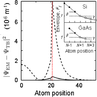
where the actual ground state depends on the width of the quantum well friesen07 . Here, corresponds to the Bloch function for the lowest band of the two-band model friesen07 , while the cosine and sine functions describe the exponential phase factors in Eq. (1), corresponding to the cases , respectively. The envelope coefficient is determined from the correspondence with Eq. (3). The physics of valley coupling is captured by the sudden change of slope (i.e., the kink) in the envelope at the interface. To facilitate calculations, we consider the model parameters shown in the inset of Fig. 1. Immediately adjacent to the interface, the envelope function exhibits a change of slope, with and on either side of the kink, and amplitude right at the interface. Thus, , , and so on.
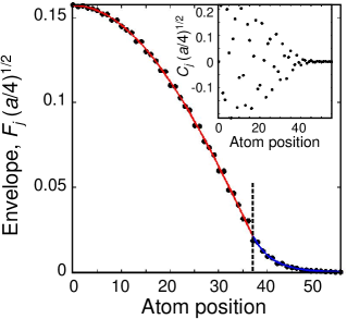
Before solving the multiscale theory, it is illuminating to gauge the accuracy of the EM ansatz of Eqs. (7)-(8). This is accomplished in Fig. 2, using the two lowest-energy TB eigenstates to infer the envelope function from the relation . The result exhibits residual short wavelength structure, arising from the fact that the exact values of the fast oscillations of the two lowest eigenstates are nearly (but not quite) identical boykin04b . This is a signature of the incomplete separation of the long and short wavelength physics, and it places a fundamental limit on our ability to match the TB and EM theories. In the present work, the spurious “jitter” evident in Fig. 2 leads to errors in the evaluation of the kink.
The multiscale theory involves just two equations from the full TB Hamiltonian, and we can choose which equations to use. The spurious jitter in Fig. 2, could be mitigated by an averaging procedure. Indeed, in this way, we obtain excellent agreement with previous estimates of the valley splitting friesen07 . However, such techniques detract from the simplicity of the multiscale approach. Here, we take a different tack, noting that the alternating behavior of the TB coefficients in Fig. 2 can be partially mitigated simply by using alternating TB equations. We consider the following equations centered symmetrically around the interface:
| (9) | |||||
Note that either the cosine (7) or sine (8) functions can be used here.
It is necessary to take into account the curvature of the envelope functions in system (9), in order to avoid unphysical solutions. Near the interface, the cosine envelope in Eq. (3) has a vanishing second derivative, but the exponential envelope does not. To leading order, we can express the latter in terms of parameters and as follows: , , and . Evaluating system (9), we now obtain
where we have dropped higher order terms in the small parameter . The anticipated linear dependence of on friesen07 emerges from Eq. (4):
| (11) |
where is in units of eVm when is in eV.
Eq. (11) is our main result, obtained through a multiscale analysis of the kink of the envelope function. We can compare this with the apparent kink obtained by fitting Eq. (3) to the full TB envelope function, as shown in Fig. 2. In spite of the spurious jitter, the two estimates agree to within 20%, in the wide quantum well limit. We can also compare Eq. (11) to the estimate obtained in Ref. [friesen07, ], by fitting theoretical EM predictions to TB numerical solutions for the valley splitting. The latter differs from Eq. (11) by about a factor of two, which we attribute to the fundamental limitations of the EM ansatz of Eqs. (7)-(8). Nevertheless, it is clear that the EM theory and the multiscale analysis, described here, capture the essential physics of valley splitting, and enable semi-quantitative predictions. Thus justified, the more accurate numerical estimate for in Ref. [friesen07, ] forms the basis for a fully quantitative EM theory. Further improvements in the EM ansatz and the kink analysis should lead to better correspondence between the estimates for .
We now turn to direct gap materials, such as GaAs. Although a sharp confinement potential does not cause valley coupling in this case, there are still atomic scale corrections to the EM theory. As in the Si case, the corrections tend to be more significant for narrow quantum wells long . Foreman has also noted that the corrections can be treated within the EM theory by introducing a -function at the interface foreman05 . Here, we apply the multiscale theory developed for Si to the GaAs quantum well, obtaining an analytical expression for the GaAs interface potential, . We also compare the improved wavefunction solutions to those obtained from TB theory.
The simplest TB theory for a single ()-valley material involves just the nearest-neighbor tunneling parameter , where Å is the width of the GaAs cubic unit cell. For AlxGa1-xAs, used in the barriers, the effective mass depends on the composition to a greater degree than silicon alloys. Hence, depends on the atomic position. The onsite parameter also depends on composition. However, for the sake of transparency, we will ignore effective mass variations, taking , and setting to an appropriate average of the effective masses near the interface. Indeed, eventually drops out of the leading order expression for , and a more careful treatment provides only small corrections.
The matching condition, Eq. (4), also hold for GaAs. However, because there is only one valley, and the TB model has only one band, the TB envelope function and wavefunction are now identical: . Near the interface, we parametrize the envelope as shown in the inset of Fig. 1. The TB eigenstates are smooth (in contrast with Fig. 2), so we may now use adjacent TB equations:
| (12) |
In this case, there is no need to consider curvature of the wavefunction. Solving for and directly, and noting the relation between the TB and EM energies, we obtain the GaAs result,
| (13) |
In the physically relevant limit of , the GaAs and Si interface potentials have identical forms. For GaAs materials parameters, we obtain .
The effect of the interface potential on the wavefunction is shown in Fig. 1, where we plot the differences between the approximate (multiscale) and exact (TB) results for a narrow quantum well. We also show results for the conventional () EM theory. Deviations from the EM theory are small in both cases. However because there is no jitter in the GaAs TB envelope function, we find that Eq. (13) captures the atomic scale corrections with great accuracy.
In conclusion, we have demonstrated that leading corrections to the effective mass theory at a sharp quantum well boundary arise from the atomic scale physics near the interface. The corrections appear as a small kink in the envelope function. A multiscale approach, combining effective mass and tight binding theories, leads to an analytical expression for the effective interface potential in silicon, which determines the valley splitting. Similar corrections apply to GaAs quantum wells, although there is no valley coupling. For other device geometries, including graded interfaces and electric fields, the present approach remains robust. These situations may also be treated by a multiscale analysis.
This work was supported by NSA/ARO contract no. W911NF-04-1-0389 and by NSF grant nos. DMR-0325634, CCF-0523675, and CCF-0523680.
References
- (1) I. Zutic, J. Fabian, and S. Das Sarma, Rev. Mod. Phys. 76, 323 (2004).
- (2) D. Loss and D. P. DiVincenzo, Phys. Rev. A57, 120 (1998).
- (3) B. E. Kane, Nature (London) 393, 133 (1998).
- (4) T. Ando, A. B. Fowler, and F. Stern, Rev. Mod. Phys. 54, 437 (1982).
- (5) S. Goswami, K. A. Slinker, M. Friesen, L. M. McGuire, J. L. Truitt, C. Tahan, L. J. Klein, J. O. Chu, P. M. Mooney, D. W. van der Weide, R. Joynt, S. N. Coppersmith, and M. A. Eriksson, Nat. Phys. 3, 41 (2007).
- (6) M. Friesen, P. Rugheimer, D. E. Savage, M. G. Lagally, D. W. van der Weide, R. Joynt, and M. A. Eriksson, Phys. Rev. B67, 121301(R) (2003).
- (7) V. N. Smelyanskiy, A. G. Petukhov, and V. V. Osipov, Phys. Rev. B72, 081304(R) (2005).
- (8) W. Kohn, in Solid State Physics, edited by F. Seitz and D. Turnbull (Academic Press, New York, 1957), Vol. 5.
- (9) F. J. Ohkawa and Y. Uemura, J. Phys. Soc. Japan 43, 907 (1977); ibid, 43, 917 (1977).
- (10) L. J. Sham and M. Nakayama, Phys. Rev. B20, 734 (1979).
- (11) M. Friesen, Phys. Rev. Lett. 94, 186403 (2005).
- (12) D. Ahn, Journ. Appl. Phys. 98, 033709 (2005).
- (13) M. Friesen, S. Chutia, C. Tahan, and S. N. Coppersmith, Phys. Rev. B75, 115318 (2007) .
- (14) T. B. Boykin, G. Klimeck, M. A. Eriksson, M. Friesen, S. N. Coppersmith, P. von Allmen, F. Oyafuso, and S. Lee, Appl. Phys. Lett. 84, 115 (2004).
- (15) T. B. Boykin, G. Klimeck, M. Friesen, S. N. Coppersmith, P. von Allmen, F. Oyafuso, and S. Lee, Phys. Rev. B70, 165325 (2004).
- (16) M. G. Burt, J. Phys. Cond. Mat. 4, 6651 (1992); M. G. Burt, Phys. Rev. B50, 7518 (1994).
- (17) B. A. Foreman, Phys. Rev. B72, 165345 (2005).
- (18) M.O. Nestoklon, L.E. Golub, and E.L. Ivchenko, Phys. Rev. B73, 235334 (2006).
- (19) H. Fritzsche, Phys. Rev. 125, 1560 (1962).
- (20) W. D. Twose, in the Appendix of Ref. [fritzsche, ].
- (21) J. H. Davies, The Physics of Low-Dimensional Semiconductors (Cambridge Press, Cambridge, 1998).
- (22) F. Long, W. E. Hagston, and P. Harrison, in 23rd International Conference on the Physics of Semiconductors, edited by M. Sheffler and R. Zimmermann (World Scientific, Singapore, 1996) p. 819.