Transport in Silicon Nanowires: Role of Radial Dopant Profile
Journal of Computational Electronics X:YYY-ZZZ,200?
©2006 Springer Science Business Media, Inc. Manufactured in The Netherlands
Transport in Silicon Nanowires: Role of Radial Dopant Profile
TROELS MARKUSSEN1, RICCARDO RURALI2, ANTTI-PEKKA JAUHO1,3, MADS BRANDBYGE1
1MIC - Department of Micro and Nanotechnology, NanoDTU, Technical University of Denmark
2Departament d’Enginyeria Electronica, Universitat Autonoma de Barcelona, Spain
3Laboratory of Physics, Helsinki University of Technology, P.O. Box 1100 FI-02015 HUT,
Finland
troels.markussen@mic.dtu.dk, Riccardo.Rurali@uab.cat, antti@mic.dtu.dk, mbr@mic.dtu.dk
Abstract. We consider the electronic transport properties of phosphorus (P) doped silicon nanowires (SiNWs). By combining ab initio density functional theory (DFT) calculations with a recursive Green’s function method, we calculate the conductance distribution of up to 200 nm long SiNWs with different distributions of P dopant impurities. We find that the radial distribution of the dopants influences the conductance properties significantly: Surface doped wires have longer mean-free paths and smaller sample-to-sample fluctuations in the cross-over from ballistic to diffusive transport. These findings can be quantitatively predicted in terms of the scattering properties of the single dopant atoms, implying that relatively simple calculations are sufficient in practical device modeling
Keywords: Silicon nanowires, dopant scattering, DFT transport calculations, mean-free path, sample-to-sample fluctuations
1. Introduction
The continuous reductions in feature sizes in the semiconductor industry have generated much interest in novel one-dimensional nanostructures such as silicon nanowires (SiNWs) [1, 2]. Scattering by defects or dopants will be increasingly important with decreasing sizes, and at the same time sample-to-sample variations become a crucial issue: when the device length and the mean free path are comparable, and shorter than the coherence length, variations of the positions of the individual dopant atoms can affect the conductance of the wire significantly. Accurate models for the electronic transport properties of nanowires including sample-variations are clearly desirable.
The mathematical theory of the conductance of disordered quasi one-dimensional systems has reached a high level of understanding in the diffusive as well as the localization regime [3, 4]. The diffusive regime is characterized by with and being the sample length, mean free path (MFP) and localization length, while in the localization regime . The universal conductance fluctuations (UCF) is a remarkable property of disordered systems: In the diffusive regime the sample-to-sample variations are described by a Gaussian distribution with universal width of the order of independent on the shape of the conductor and type of disorder [5].
Several recent theoretical works used density-functional theory (DFT) to consider the energetics of dopants in SiNWs [6, 7]. Further, Fernandez-Serra et al.[8] considered scattering properties of single phosphorus (P) dopants. In a recent work [9] we studied sample-averaged conductance properties (, std(), MFP) in long SiNWs containing a random distribution of either B or P dopants along the wire. In this work we continue the analysis focusing more on the conductance distribution and on the influence of the radial dopant profile.
2. Method
In this work we model the conductance properties of SiNWs with randomly distributed P dopant atoms. The wires are oriented along the direction and are surface passivated by hydrogen atoms to avoid dangling bonds. The Hamiltonians describing the pristine wire as well as regions containing dopant impurities are obtained using ab initio density-functional theory (DFT) calculations [11]. The DFT calculations on the doped regions use supercells containing nine wire unit cells (837 atoms) with a total length of 50.4 Å and with the single dopant atom placed in the middlemost unit cell. The atomic positions of all the atoms in the central unit cell containing the dopant atom as well as the two neighboring unit cells have been fully relaxed, until the maximum force was smaller than 0.04 eV/Å. The large super cell ensures that the there is no dopant-dopant interaction and that the electronic structure at the supercell-supercell interface is very close to that of the pristine wire. The length and energy dependent conductance of a long wire with randomly placed P atoms is calculated using a standard recursive Green’s function (GF) method [10]. In each recursion step, we add a unit cell from either the pristine wire or from a region around a dopant atom. At each energy we do this calculation for 560 different realizations of the dopant positions to obtain the conductance distribution. By changing the relative occurrence of different dopant positions, we can model different radial dopant profiles. In all calculations we use an average dopant-dopant separation nm corresponding to a bulk doping density of cm-3. Since P dopants are n-type we consider only energies in the conduction band and measures all energies relative to the conduction band edge, .
3. Single-dopant results and estimates
Fig. 3. shows the transmission vs. energy through infinite wires containing only a single P dopant atom placed at five different substitutional positions (1-5) indicated in the inset. The P dopants located in the bulk positions (1-3) generally scatter the electrons more than the surface positions (4-5).
In a recent work [9] we showed that the sample-averaged properties, , std() and MFP could be accurately predicted using information only from the single-dopant transmissions shown in Fig. 3.. We define an average scattering resistance
| (1) |
where and is the contact resistance with being the number of conducting channels at energy . The first term on the right is the average of the single-dopant conductances taking the probability, , of each dopant position into account. In the present study , corresponding to the five different dopant positions shown in the inset in Fig. 3.. Denoting the average dopant-dopant distance, , the average resistance of a wire of length, , is estimated as
| (2) |
From the linear region of the vs. curves (see Fig. 4. (a)) one can extract the energy dependent MFP, through the relation
| (3) |
Comparing (2) with (3) we obtain an expression for the MFP given only by the single-dopant transmissions, the doping-dopant distance, and the dopant distribution:
| (4) |
We emphasize that the relations above only hold for wire lengths shorter than the localization length, . We can calculate using the relation [4],
| (5) |
which now can be estimated using the single-dopant result, [9].
4. Long wire results
Fig. 4. shows the conductance distribution for different wire lengths at energy eV (a)-(d) and eV (e)-(h). The radial dopant distribution is uniform, i.e. the positions 1-5 are equally likely. The conductance distribution at the higher energy (left) develops from a quasi-ballistic regime (a) with a few peaks in the histogram, to the diffusive regime (b)+(c) and finally to the beginning of the localization regime (d).
In the diffusive regime the conductance distribution is well described by a Gaussian with the standard deviation being close to the universal conductance fluctuation (UCF) value of . In the ballistic and diffusive regimes, the sample averaged resistance increases linearly with wire length, as illustrated in Fig. 4. (a) (circles). For wire length nm the resistance starts to increase above the initial linear behavior, thus entering the localization regime. Notice that the localization sets in when in agreement with Thouless’ argumentation [12]. The resistance of the surface-doped wires Fig. 4. (a) (stars) increases linearly throughout the length range and stays in diffusive regime. The two solid lines in Fig. 4. (a) obtained using (2) clearly resemble the sample-averaged values (circles and stars) in the linear regimes. This demonstrates, that the average resistance in the ballistic- and diffusive regimes can be accurately predicted for various dopant distributions only based on the single-dopant scattering properties.
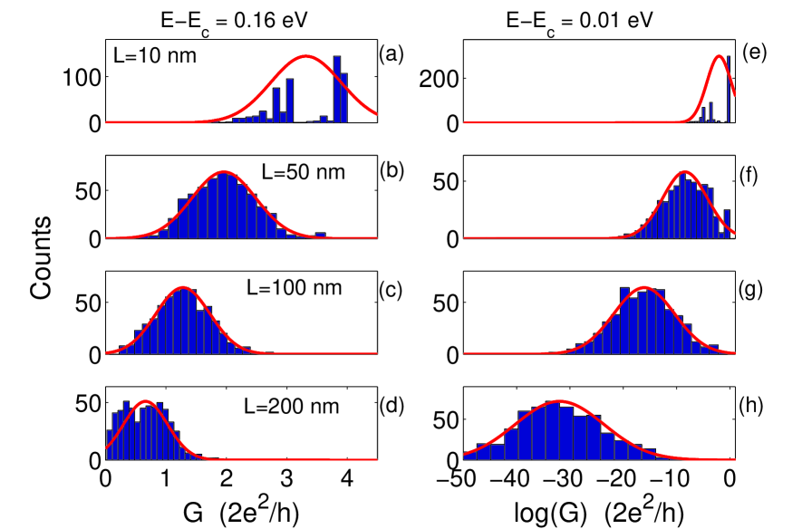
In the distribution plots the diffusive-localization transition starts when the low conductance tails of the histograms come close to zero and starts to ’pile up’. Eventually the distribution develops into a log-normal distribution. This is further illustrated in the right part (e)-(h) showing the distribution of log() at the energy eV just above the conduction band edge.
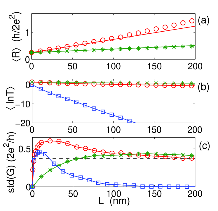
The transmission, , decreases as for wires in the localization regime. This is illustrated in Fig. 4. (b) showing vs. at eV (squares) and at eV for the uniformly doped wires (circles) and the surface doped wires (stars). The localization length is obtained from the slopes in the final linear regions. At eV we get nm and for the uniformly doped wire at eV we find nm. The surface doped wire does not reach a linear region in the considered length range and we can only say that nm. The calculated localization lengths generally agree with the relation (5) giving and nm at and eV respectively.
The length dependences of the sample-to-sample variations, std(), shown in Fig. 4. (c) are qualitatively different for the two radial dopant distributions. The purely surface doped wires (stars) approach the UCF level (horizontally dashed line) from below. On the other hand, the uniformly doped wires (circles) reaches a clear maximum before the UCF level is approached from above. A similar maximum is observed at eV (squares). Both maxima occur around , which seems to be a quite general result independent of energy and dopant concentration [9].
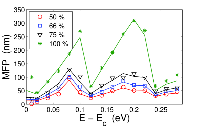
Using (3) we extract the MFP from the linear regions in Fig. 4. (a). By doing this at many energies, we obtain the energy dependent MFP shown in Fig. 4.. The different markers correspond to different surface-dopant fractions. The solid lines are obtained from the single-dopant calculations using (4) and correspond to the same surface dopant fraction as the closely lying markers. We see that the single-dopant estimates accurately resemble the sample-averaged results over the entire energy range. At all energies, the MFP increases with increasing surface dopant fraction, and at pure surface doping the MFP is on average more than three times larger than for uniform doping. The large increase in MFP for surface doped wires might be useful for device applications. However, there are potential problems with dopants close to the surface as they can be passivated by extra hydrogen atoms and thereby no longer provide extra carriers [8].
5. Conclusion
By combining ideas of scaling theory and universal conductance fluctuations with DFT and Landauer formalism we have analyzed the conductance properties of SiNWs. We have studied the transport in phosphorus doped SiNWs by computing the sample averaged conductance, mean free path (MFP), localization length, and sample-to-sample variations as a function of Fermi energy, radial doping distribution, and wire length. The MFP was significantly increased in surface doped wires as compared to more uniform dopant distributions. Moreover, the sample-to-sample variations at wire lengths were smaller in the surface doped wires. These results can be understood and accurately estimated from the scattering properties of the single dopants, implying that relatively simple calculations are sufficient in practical nanoscale device modeling.
Acknowledgment
We thank the Danish Center for Scientific Computing (DCSC) for providing computer resources. APJ is grateful to the FiDiPro program of the Finnish Academy for support during the final stages of this work. RR acknowledges financial support from Spain’s Ministerio de Educación y Ciencia Juan de la Cierva program and funding under Contract No. TEC2006-13731-C02-01.
References
- [1] Y. Cui, Z. Zhong, D. Wang, W. U. Wang, and C. M. Lieber, High performance silicon nanowire field effect transistors, Nano Letters 3, 149 (2003).
- [2] F. Patolsky and C. M. Lieber, Nanowire nanosensors, Materials Today 8, 20 (2005).
- [3] P. A. Lee and T. V. Ramakrishnan, Disordered Electronic Systems, Reviews of Modern Physics, 57, 287, (1985)
- [4] C. W. J. Beenakker, Random-matrix theory of quantum transport, Rev. Mod. Phys. 69, 731 (1997).
- [5] P. A. Lee and A. D. Stone, Universal conductance fluctuations in metals, Physical Review Letters, 55, 1622, (1985)
- [6] M. V. Fernandez-Serra, C. Adessi, and X. Blase, Surface segregation and backscattering in doped silicon nanowires, Physical Review Letters 96, 166805 (2006).
- [7] H. Peelaers, B. Partoens, and F. M. Peeters, Formation and segregation energies of B and P doped and BP codoped silicon nanowires, Nano Letters 6, 2781 (2006).
- [8] M. V. Fernandez-Serra, C. Adessi, and X. Blase, Conductance, surface traps, and passivation in doped silicon nanowires, Nano Letters 6, 2674 (2006).
- [9] T. Markussen, R. Rurali, A.-P. Jauho, and, M. Brandbyge Scaling theory put into practice: First-principles modeling of transport in doped silicon nanowires, Physical Review Letters 99, 076803 (2007).
- [10] T. Markussen, R. Rurali, M. Brandbyge, and, A.-P. Jauho Electronic transport through Si nanowires: Role of bulk and surface disorder, Physical Review B 74, 245313 (2006).
- [11] J. M. Soler, E. Artacho, J. D. Gale, A. Garc a, J. Junquera, P. Ordejon, and D. Sanchez-Portal, The SIESTA method for ab initio order-N materials simulation, Journal of Physics: Condensed Matter 14, 2745 (2002).
- [12] D. J. Thouless, Maximum metallic resistance in thin wires, Physical Review Letters, 39, 1167, (1977).