Sideband cooling and coherent dynamics in a microchip multi-segmented ion trap
Abstract
Miniaturized ion trap arrays with many trap segments present a promising architecture for scalable quantum information processing. The miniaturization of segmented linear Paul traps allows partitioning the microtrap in different storage and processing zones. The individual position control of many ions - each of them carrying qubit information in its long-lived electronic levels - by the external trap control voltages is important for the implementation of next generation large-scale quantum algorithms.
We present a novel scalable microchip multi-segmented ion trap with two different adjacent zones, one for the storage and another dedicated for the processing of quantum information using single ions and linear ion crystals: A pair of radio-frequency driven electrodes and 62 independently controlled DC electrodes allows shuttling of single ions or linear ion crystals with numerically designed axial potentials at axial and radial trap frequencies of a few MHz. We characterize and optimize the microtrap using sideband spectroscopy on the narrow qubit transition of the 40Ca+ ion, demonstrate coherent single qubit Rabi rotations and optical cooling methods. We determine the heating rate using sideband cooling measurements to the vibrational ground state which is necessary for subsequent two-qubit quantum logic operations. The applicability for scalable quantum information processing is proven.
pacs:
37.10.Ty, 37.10.-x, 32.80.Qk, 03.67.Lx1 Introduction
Long term goal of our research is the large-scale quantum computer [1, 2] with multiple ions and linear ion crystals for encoding complex entangled states, with optimized laser pulses for processing quantum information (QIPC), and with well suited time-dependent trap control voltages to shuttle quantum information between a central processing unit and quantum memories or qubit read-out sections. On the way towards this goal we present in this paper the most complex microstructured ion trapping device with a large number of control segments such that in future order of 102 qubits might be processed. Currently we do not exploit at all the complexity of our segmented trapping device and the corresponding options for large-scale quantum processing. The purpose of this paper, however, is describing the trap device, characterizing its basic performance and proving necessary building blocks for quantum gates with ions.
The work presented here should be seen in context with pioneering work to fabricate specialized ion microtraps for QIPC (instead of using mm-sized conventional designs [3, 4, 5, 6]) by using microscale planar [7, 8], linear three-dimensional [9, 10, 11] or even more complex geometries [12]. Gold plated substrates allow electrode structures with gaps of a few m, but semiconductor structuring may allow in future even finer and more complex traps [13]. Shuttling protocols for single ions [14, 15, 16, 17] have been tested and even used for implementing quantum algorithms [18, 19]. On the other hand, the application of well controlled laser pulses has lead to the entanglement of up to eight ions [20] and the realization of complex quantum algorithms like e.g. teleportation [21].
The paper is organized as follows: First we outline the steps for the fabrication of the multi-segmented linear ion trapping device and the integration in the overall experimental setup. Cold crystals of trapped 40Ca+ ions are showing the elementary operation of this device. For refined studies of trapped ions and the properties of the trap we employ quantum jump spectroscopy on the narrow quadrupole transition, where all components of the ion motion are resolved easily. Investigating the micromotional sideband allows shifting of the ion to the center of the radio-frequency (RF) trapping field. Since we are observing a very small variation of the necessary compensation voltage only we conclude that charging effects are indeed effectively impeded by the advanced trap construction. If the ion is excited by a narrow band laser source, we observe Rabi flopping as we vary the pulse duration. Finally, we study the secular sidebands and sideband cool a single ion from Doppler temperature down to the vibrational ground state. Cooling time and trap heating time are revealed. Finally, in section 5, we sketch future applications.
2 Microchip ion trap
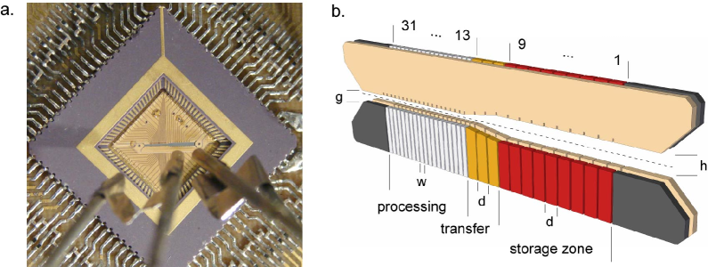
The Ulm microchip trap is a two-layer electrode design modeled as logical continuation of conventional linear Paul traps (figure 1a). The storage zone is connected to the processing zone by a multi-segment transfer region in order to achieve a smooth passage avoiding vibrational excitation (figure 1b). The electrode layers are as symmetric as possible for well-balanced electric potentials on the trap axis such that micromotion should be minimized. Thus, the non-segmented RF segments are cut with notches precisely opposite to the separation cuts in the DC electrodes to improve the axial electric field symmetry. The microtrap is assembled in a UHV compatible ceramic chip carrier with the advantage of an exceptional alignment precision of the electrode layers. Furthermore easy electric connectivity, exchange usability and in the near future the integration in UHV compatible electronic boards with fast digital-analog converters and digital RF synthesizers prioritize this proof of concept.
2.1 Design and fabrication
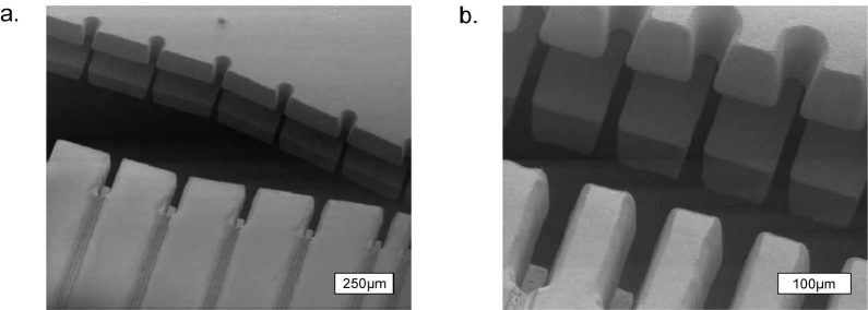
The Ulm microtrap is based on a geometric three-layer stack design fabricated using gold coated and laser structured Al2O3 wafers222Reinhardt Microtech AG, Wangs, Switzerland. The development process of the wafers starts with micro-machining of blank wafers (figure 2a) using a femtosecond pulsed laser source333Micreon GmbH, Hannover, Germany. In the storage zone the central slit width is h=500m, while the transfer region narrows the slit to g=250m according to the width of the processing zone (figure 1b). The central slit in the storage/transfer zone and the processing zone is bounded by the DC electrode fingers with a width of d=250m and w=100m separated with a spacing of 30m. The constant length of the DC electrode fingers is 200m. The length of the RF notches with 60m is optimized for mechanical stability and provides the axial field symmetry with a 30m spacing. Additional holes with a diameter of 240m in the outer region allows alignment and mounting.
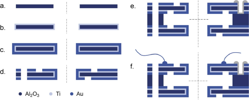
The wafer metallization is done after a careful ultrasonic cleaning procedure (acetone, isopropyl, piranha) and an oxygen plasma cleaning. The laser cutted blank Al2O3 wafer is coated in an electron beam evaporator during a continuous rotation with 50nm titanium and 500nm gold (figure 2b and c). A declination angle of 45∘ is required during the coating process for an overall continuous coating. The surface roughness is better than 10nm, which was verified by atomic force microscopy. The conductor paths are manufactured by laser structuring of the wafer metallization (figure 2d). Finally, the wafer is laser diced. Bottom, center and top layer of the microtrap are aligned and mounted with UHV compatible UV epoxy adhesive (figure 2e). The stack of three layers is mounted in a center holed UHV compatible leadless ceramic 84-pin chip carrier444Kyocera, type LCC8447001 with outer dimensions of 30mm squared and an inner cavity size of 12mm. Electrical connections to the ceramic chip carrier rely on ball bonding with 15m diameter gold wire (figure 2e). Our design avoids dielectric blank Al2O3 areas, unavoidable isolation lines between the electrode segments are shifted away 200m from the ions position by the extended electrode finger design. From an electron microscopy analysis we checked that the DC electrode finger segments are gold plated completely from all sides.
The microtrap chip carrier is mounted on a low-pass filter printed circuit board (PCB), that serves as electrical connector device of the 80-pin ribbon cables. The PCB is based on the UHV compatible polyimide laminate Isola P97555Isola GmbH, Düren, Germany, which is 200m gold electroplated. The UHV compatible Kapton ribbon cables are connected with ceramic D-type connectors in vacuum. Low-pass filters (ceramic SMD type) with a cutoff close to 10MHz are soldered close to the chip carrier (figure 1a).
Decreasing electrode geometries of the processing zone compared to the storage zone of the microtrap has some advantages with respect to quantum information experiments: A smaller electrode design provides stronger confinement of the ions at the same voltage levels. Stronger confinement leads to higher axial vibration frequencies, which set the time scale for multi-qubit gate operations. For the details of the trapping fields in axial and radial direction we use numerical simulations.
2.2 Field simulations
The trap region of the microtrap is partitioned into a 9-segment loading and storage section, a 3-segment transfer region and a 19-segment processing zone. Each electrode pair of a segment is voltage controlled separately, providing a full control for each trap site individually and an effective micromotion compensation. Numerical simulations give insight how to form potentials suitable to trap single ions or linear crystals (figure 4). The loading zone is optimized such that a thermal beam of calcium passes through, therefore the cross section of the storage zone is asymmetric with a ratio 4:1. The more symmetric cross section of the processing zone with a ratio 2:1 leads to a strong confinement of the ions and higher radial and axial frequencies [22].
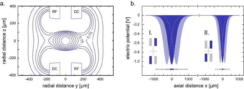
The 2D dynamical confinement in the radial cross section at the storage region (figure 4a) is described numerically by the quadrupole potential strength of the dynamical trap potential . The lowest-order approximation shows the geometric factor of the quadrupole potential strength (yz cross section). The storage region is characterized by ; the processing region shows a stronger confinement with . Under typical operating conditions, see section 3.1 and with the trap drive frequency denoted by , the dimensionless stability parameter results in for the storage and for the processing region. The calculated simplified frequency of the secular motion in the storage region is 1.26MHz and is reproduced experimentally with high accuracy. The measurements presented here are implemented in the storage region, so the processing region allows a tighter confinement of the ion in future experiments.
The axial potential along the trap axis is calculated in a numerical three-dimensional electric potential simulation (figure 4b). Requirements for fast ion transport are deep axial potentials with moderate control voltages and a large spatial overlap of the axial potentials from adjacent electrode pairs [22]. The peak width at half-height of the axial potentials are 500m at the storage region (250m segment width) and 264m at the loading region (100m segment width). For the wider segments of 250m in the storage zone the trap allows a tight confinement with an axial frequency of 1.20MHz with -5V applied only, which is experimentally verified within 5% accuracy via sideband spectroscopy.
3 Experimental set-up
3.1 Trap operation
For the RF supply of the trap a RF synthesizer is used, followed by a an amplifier to feed +26dBm (400mW) power into a helical resonator matching the 50 amplifier output impedance with the trap. The injected RF power is monitored by an capacitive divider. Under typical operating conditions we reach amplitudes of 280Vpp at a frequency of 24.841MHz. The DC electrodes are supplied with voltages in the range of 10V. Here the ion is trapped in the middle of the storage region with one electrode pair; the trap electrodes and the adjacent pairs are biased for micromotion compensation. The trap is installed in a stainless steel DN200CF vacuum chamber with a regular octagon DN63CF viewport symmetry. With a pump system comprising an 75l ion pump and a titanium sublimation pump we operate the experiment at a pressure of 10-10mbar. Pairs of magnetic field coils in a three-axis Helmholtz configuration are used for compensating the stray magnetic fields and generating a quantization axis with a magnetic field of 0.3mT directed at -45∘ with the trap axis x.
3.2 Laser configuration
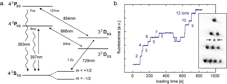
Single 40Ca+ ions stored in the trap are generated by photoionization of a neutral calcium atomic beam from a resistively heated oven. The two step process is driven by laser light near 423nm and 375nm [23]. Figure 5a shows the level scheme of 40Ca+: The Dipole transitions 42S 42P1/2 at 397nm allows Doppler cooling of the ions, the 32D 42P1/2 near 866nm and the transition 32D 42P3/2 near 854nm the depletion of the metastable D-levels. The quadrupole transition near 729nm from the 42S1/2 ground state to the metastable 32D5/2 level is employed for sideband spectroscopy, sideband cooling and coherent quantum dynamics.
All transitions of the 40Ca+ ion are driven by grating stabilized diode lasers. The lasers at 397nm, 866nm and 854nm are locked to external Zerodur Fabry-Perot cavities (finesse F=250) for frequency stabilisation using the Pound-Drever-Hall (PDH) technique. The laser at 729nm (laser diode followed by a tapered amplifier) is PDH-locked to a cavity with finesse reaching a sub-kilohertz linewidth; the cavity is fabricated from ultra low expansion glass (ULE) material. Lasers at 866nm, 854nm and 729nm can be switched off using acousto-optical modulators in double-pass configuration, also being employed for tuning the laser frequency near 729nm. Laser beams at 397nm, 866nm and 854nm are within the xy plane (see figure4) and intersect the trap at 45∘ with respect to the trap axis x. A separate beam is deviated from the laser near 397nm for optical pumping. Also this beam lies in the xy plane but intersects the trap axis under -45∘, parallel to the magnetic field direction. The beam near 729nm, in the xy plane, is focused to a waist size of 15m and intersects the trap under 45∘ perpendicular to the magnetic field axis. The Lamb-Dicke factor of excitation depends on the projection of the vector on the trap axis as well as the trap frequency 1.1MHz and mass m of the ion like and we calculate =0.065. The polarization at 729nm is chosen such that only m=2 transitions are allowed, e.g. from , m=+1/2 to , m=+5/2 and m=-3/2.
3.3 Doppler cooling, fluorescence detection and cold ion crystals
The ion fluorescence is imaged by a custom lens system666Sill Optics, Wendelstein, Germany (focal length 66.8mm, numeric aperture 0.27) on an EMCCD camera777iXon DV860-BI, Andor Technology, Belfast, Northern Ireland (efficiency of 50%) and a photomultiplier tube (PMT) of quantum efficiency 27% for detecting ions and reading out the quantum state. The magnification of the imaging branch is roughly 20. The fluorescent light is collected from a solid angle of 2.5%. It is distributed at a ratio of 80:20 between PMT and camera by a beam splitter and filtered by a band pass filter to suppress background photons. For trapping and cooling, 1mW of 866nm light is focussed to a spot size of 30m. The power of the laser near 397nm is focussed to a spot size of 20m and can be switched between zero, a reduced power level of 30W (Doppler cooling) and full power of about 300W (detection). With the laser slightly red detuned and proper micromotion compensation, a single ion count rate of 16kHz at a background of 4kHz can be achieved with the PMT. If an ion is shelved in the long lived D5/2 level, no light is scattered. With a detection time of 5ms, we are able to discriminate the qubit states with an error probability of [5]. Figure 5b shows linear ion crystals trapped and observed in the microtrap.
4 Quantum jump spectroscopy
Quantum jump spectroscopy has been used to determine the frequency of clock transitions with an accuracy of about 7 parts in 10-17 [24, 25, 26, 27]. A narrow dipole forbidden transition is driven and subsequently the excitation to the metastable level is tested by exposure to resonant radiation on a dipole allowed transition.
4.1 Sideband spectroscopy on the S1/2 to D5/2 transition
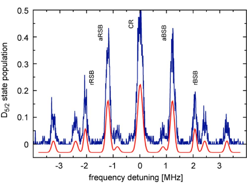
In the experiments presented here, we perform spectroscopy on the S1/2 to D5/2 transition (figure 6). With a lifetime of 1.2s, the spectroscopic resolution is limited by the laser pulse duration, the Rabi frequency during the excitation and the frequency stability of the laser source. The harmonic motion of the ion in the trap can be investigated spectroscopically at the level of single vibrational quanta. The electronic and vibrational state is manipulated coherently with the following sequence:
-
1.
Doppler cooling: the laser near 397nm is red detuned from the S1/2 to P1/2 transition to 1/2 of the maximum fluorescence rate. This corresponds to a setting of about where =(2) 22.3MHz is the natural linewidth of the dipole transition. The beam is attenuated in order to avoid saturation. The laser frequency near 866nm is tuned for maximum fluorescence. Additionally, resonant laser light depopulates the metastable D5/2 level. Typically we apply Doppler cooling for 5ms. While the theoretical cooling limit results in a mean phonon number of , with 12, typically we observe a slightly higher between 12 and 25.
-
2.
Optical pumping: with a typically 5s short pulse of polarized light near 397nm we pump the ion into the S1/2, m=+1/2.
-
3.
Sideband cooling (optionally): we tune the laser light near 729nm such that the red secular sideband of the S1/2, m=+1/2 to D5/2, m=+5/2 is excited. The D5/2 state is quenched by resonant laser light near 854nm to the P3/2 level which quickly decays to S1/2 closing the cooling cycle. Short pulses of optical pumping as in step (ii) are inserted into, and also conclude the sideband cooling.
-
4.
Spectroscopy pulse: all laser sources, except the laser light near 729nm, are switched off. We excite the S1/2, m=+1/2 to D5/2 transition with pulses of well-defined frequency, duration and intensity.
-
5.
State detection: the lasers at 397nm and 866nm are switched back on. The power of the 397nm laser is at maximum such that a maximum count rate is obtained. The PMT counts photons of the ions fluorescence. If the ion had been excited on the quadrupole transition to the D5/2 level, no fluorescence photons will be observed.
The entire sequence is repeated typically 50 to 500 times depending on the requirements, and the average excitation to the D5/2 level is recorded. For measurements and an excitation probability , the projection noise error is given by . Then e.g. the laser frequency near 729nm is varied, see figure 6. Here, the ion is excited without sideband cooling step (iii) such that the radial and axial red and blue motional sidebands show equal strength. These resonances are denoted with rRSB to rBSB. Additional resonances show up at a laser detuning for a second sideband excitation and at difference frequencies of the sidebands .
4.2 Micromotion compensation
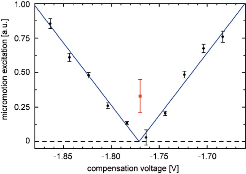
If an ion is displaced from the node of the RF electric field either by asymmetries or by patch charges, it will oscillate at the trap drive frequency . Consequently, Doppler cooling and fluorescence detection will be affected. However, micromotion is compensated by applying a balanced voltage difference to the particular segments of an electrode pair such that the ion is moved into the RF trap center. Various methods of measuring the micromotion have been studied [28]; yet another method uses sideband spectroscopy: we excite the sideband at and compare the sideband excitation with that on the carrier [5]. The Rabi frequency on the micromotion sideband and that one on the carrier holds / = J1()/() /2 for , with denoting the index of modulation and Jn indicating the Bessel functions of the n-th order. As the excitation to the D5/2 state is proportional to for low saturation, we can measure the ions micromotion directly, see figure 7. We find the minimum excitation close to -1.77V. At this minimum, thus for optimum compensation voltage, we reduce the ratio of excitation strength to zero with an error of 0.03. This measured value corresponds to the ratio of squared Bessel functions J()/J() with modulation index of , which is due to a residual micromotion oscillation amplitude x of (0130)nm. The optimal compensation voltage changes by less than 0.5% from day to day.
In conclusion, the micromotion can be nulled by a properly set compensation voltage and, due to the shielding effect of the gold-coated finger-shaped electrodes, stray electric fields from isolating parts of the microtrap do not show up with large and fluctuating contributions.
4.3 Coherent single ion dynamics
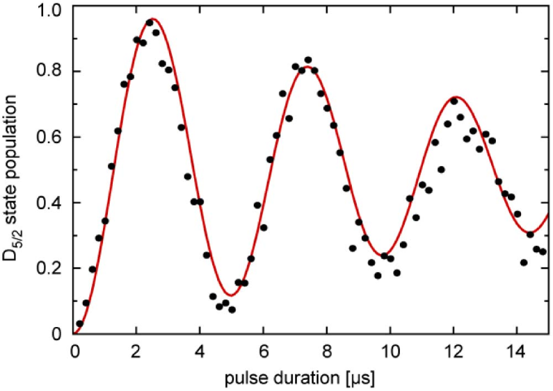
The coherent ion-light interaction leads to Rabi oscillations between the S1/2 ground state and the excited metastable D5/2 state when the duration of the interaction is varied. If the single ions internal states are used to store qubit information, a -pulse will flip the qubit between the two logic states.
Here, we present Rabi oscillations on the carrier transition for a single ion, see figure 8, which has been Doppler-cooled. The data shows a 95% efficiency for the -pulse at 2.5s, corresponding to a Rabi frequency of 200kHz. The decay of contrast is due to the fact that we observe an incoherent superposition of Rabi oscillations with a different frequency for each thermally occupied Fock state: . If we model the data with we find agreement for a thermal distribution pn with 12 (figure 8).
4.4 Sideband cooling
For Doppler cooling, the temperature limit is given by the natural linewidth of the dipole transition. For quantum logic operations, however, a mean phonon number below this limit is often required. Therefore we apply sideband cooling on the narrow S1/2 to D5/2 transition [29]. Laser radiation near 729nm on the red sideband of the transition excites from S1/2, m=+1/2 to D5/2, m=+5/2. The effective width of this cooling transition can be increased by applying resonant laser light near 854nm. This mixes the D5/2 state with the P3/2 state which rapidly decays to the S1/2, m=+1/2. The cooling rate is modified accordingly, and the effective width of the D5/2 level sets an upper limit for the rate of cooling cycles.
For the introduction of laser cooling of trapped particles we apply the semiclassical theory [30], determine all laser cooling parameters experimentally and compare the cooling result with the theoretical expectation.
The theoretical limit of sideband cooling is given by the ratio of laser cooling and the heating rates , yielding as the steady state average phonon number. Heating by laser processes is due to either an off-resonant excitation on the carrier transition with subsequent decay on the blue sideband or an off-resonant blue sideband excitation followed by a decay on the carrier [30]. A calculation of the detailed balance of phonon states leads to
| (1) |
if trap heating is excluded. Here, the parameter results in 0.17, for the axial trap frequency = 1.1MHz, as it takes into account the recoil if the ion decays spontaneously from the P3/2 level to the S1/2 ground state. Due to the laser recoil on the S1/2 to D5/2 excitation we get =0.065. In equation 1 only the cooling rate, but not the cooling limit depends on the intensity of the laser near 729nm. denotes the effective linewidth from quenching the D5/2 state to the P3/2 and is adjusted by the laser power at 854nm.
The average phonon number increases with the intensity of the laser near 854nm; thus one has a tradeoff between cooling rate and minimum temperature. However, even for 90kHz, equation 1 predicts an almost perfect ground state of vibration with only 0.01. The situation is more complicated if we take trap heating into account: the steady state photon number results from the balance
| (2) |
if the laser induced heating is small compared to the trap heating rate. We find that the thermal mean phonon number becomes
| (3) |
for the case where the net cooling rate is positive. In contrast to equation 1, the cooling limit now depends on the intensity of the laser near 729nm driving the red sideband of the quadrupole transition. We consider here the case where the sideband excitation is incoherent, with .
In order to compare the above cooling theory to the experiment, we need to determine , and in independent experimental measurement sequences and compare the theoretical prediction in equation 3 with the experimental outcome on .
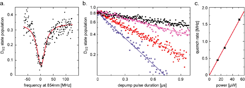
is determined by controlled depletion of the metastable state: After Doppler cooling and optical pumping, we apply a 1s laser pulse on the carrier transition such that the ion is transferred into the D5/2 state. A pulse of laser light resonant to the D5/2 to P3/2 transition is then applied and finally the remaining D5/2 population is determined. From the exponential decay, see figure 9b, we determine the effective cooling width that is as expected a linear function of the laser power at 854nm, with kHzP.
The Rabi frequency on the quadrupole transition is revealed from measurements such as in figure 8. With the maximum available laser power of 60mW we reach 200kHz. Correspondingly, the maximum possible sideband excitation with this laser power is =(2) 13kHz.
4.5 Heating rate measurement
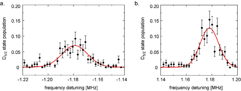
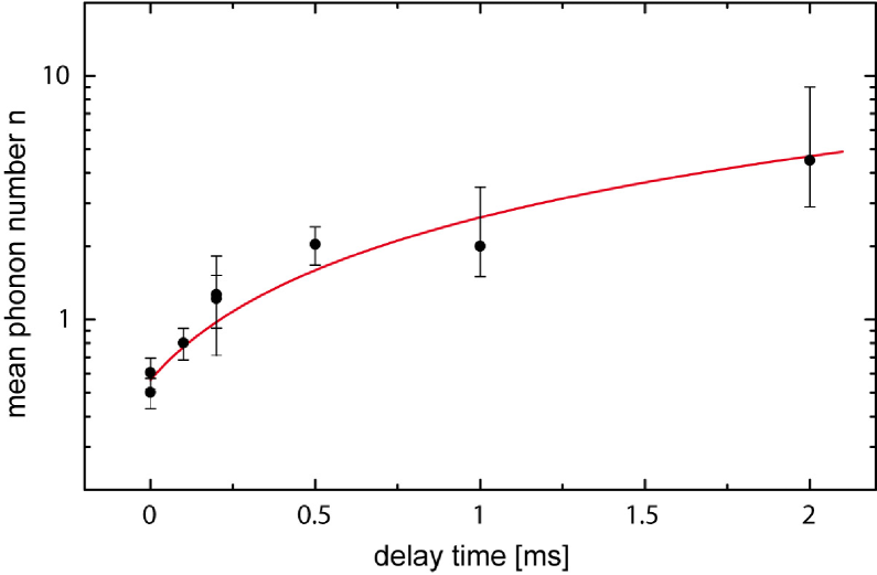
The mean phonon number of is determined from spectra such as in figure 10 showing the red and blue sideband after sideband cooling. We deduce from the ratio of the sideband intensities A=Pred/Pblue by means of the asymmetry of the excitation (figure 10) the mean phonon number , here =0.56(5). To obtain the trap heating rate, we insert a variable waiting time interval between steps (iii) and (iv) in the experimental sequence, see section 4.1 [4]. The data plotted in figure 11 yields a trap heating of 2.1(3) per ms. As this heating rate is attributed to the contamination of trap electrodes due to the loading process from the thermal beam of neutral calcium, we expect a lower mean phonon number in the processing region, which is spatially separated from the loading zone.
Note that quantum gate operations and the transport of ions in the trap are about 10 to 100 times faster than the measured trap heating. In future we will investigate the influence of the gold coating (different surface qualities and thickness) on the trap heating.
5 Conclusion and outlook
We have outlined the design, the fabrication and the first characterization of a novel multi-segmented microchip ion trap, and we have show that this trap is suited for scalable quantum logic. In some detail, the sideband cooling on the quadrupole transition has been investigated. In future, we will explore Raman transitions between Zeeman ground (qubit) states S1/2, m=+1/2 and m=-1/2 for the cooling, for coherent qubit rotations and for two-qubit gate operations. Additionally, we will study the transport of quantum information between the processor and the memory section benefiting from the large number of trap segments. Further development will include the integration of micro-optical elements.
Acknowledgements: We thank Frank Korte (Micreon GmbH) for his expertise in laser cutting, H. Roscher for the cooperation in the cleanroom facility, K. Singer and R. Reichle for their contributions in an earlier stage of the experiment, K. Singer for his important help with the experimental control software, and J. Eschner for discussions. We acknowledge financial support by the German science foundation DFG within the SFB/TRR-21 and by the European commission within MICROTRAP (Contract No. 517675) and EMALI (Contract No. MRTN-CT-2006-035369).
References
- [1] M. Nielsen and I.L. Chuang. Quantum Computation and Quantum Information. Cambridge University Press, 2000.
- [2] European and the US quantum information roadmaps are found at http://qist.ect.it and at http://qist.lanl.gov.
- [3] W. Neuhauser, M. Hohenstatt, P. Toschek, and H. Dehmelt. Optical-sideband cooling of visible atom cloud confined in parabolic well. Phys. Rev. Lett., 41:233, 1978.
- [4] C. Roos, Th. Zeiger, H. Rohde, H.C. Nägerl, J. Eschner, D. Leibfried, F. Schmidt-Kaler, and R. Blatt. Quantum state engineering on an optical transition and decoherence in a paul trap. Phys. Rev. Lett., 83:4713, 1999.
- [5] C. Roos. Controlling the quantum state of trapped ions. PhD thesis, Leopold-Franzens-Universität Innsbruck, 2000.
- [6] F. Schmidt-Kaler, H. Häffner, S. Gulde, M. Riebe, G.P.T. Lancaster, T. Deuschle, C. Becher, W. Hänsel, J. Eschner, C. Roos, and R. Blatt. How to realize a universal quantum gate with trapped ions. Appl. Phys. B, 77:789, 2003.
- [7] S. Seidelin, J. Chiaverini, R. Reichle, J.J. Bollinger, D. Leibfried, J. Britton, J. Wesenberg, R.B. Blakestad, R.J. Epstein, D. Hume, W.M. Itano, J.D. Jost, C. Langer, R. Ozeri, N. Shiga, and D.J. Wineland. A microfabricated surface-electrode ion trap for scalable quantum information processing. Phys. Rev. Lett., 96:2530031, 2006.
- [8] K.R. Brown, R.J. Clark, J. Labaziewicz, P. Richerme, D.R. Leibrandt, and I.L. Chuang. Loading and characterization of a printed-circuit-board atomic ion trap. Physical Rev. A, 75:15401, 2007.
- [9] D. Stick, W. K. Hensinger, S. Olmschenk, M. J. Madsen, K. Schwab, and C. Monroe. Ion trap in a semiconductor chip. Nature Physics, 2:36, 2006.
- [10] D. Leibfried and T. Schätz. Ein atomarer Abakus. Physik Journal, 3:23, 2004.
- [11] Q.A. Turchette, D. Kielpinski, B.E. King, D. Leibfried, D.M. Meekhof, C.J. Myatt, M.A. Rowe, C.A. Sackett, C.S. Wood, W.M. Itano, C. Monroe, and D.J. Wineland. Heating of trapped ions from the quantum ground state. Phys. Rev. A, 61:063418, 2000.
- [12] W.K. Hensinger, S. Olmschenk, D. Stick, D. Hucul, M. Yeo, M. Acton, L. Deslauriers, C. Monroe, and J. Rabchuk. T-junction ion trap array for two-dimensional ion shuttling and storage and manipulation. Appl. Phys. Lett., 88:034101, 2006.
- [13] M. Brownnutt, G. Wilpers, P. Gill, R.C. Thompson, and A.G. Sinclair. Monolithic microfabricated ion trap chip design for scalable quantum processors. New J. Phys., 8 No 10:232, 2006.
- [14] M.A. Rowe, A. Ben-Kish, B. DeMarco, D. Leibfried, V. Meyer, J. Beall, J. Britton, J. Hughes, W.M. Itano, B. Jelenkovic, C. Langer, T. Rosenband, and D.J. Wineland. Transport of quantum states and separation of ions in a dual rf ion trap. Quantum Information and Computation, 2:257–271, 2002.
- [15] R. Reichle, D. Leibfried, R.B. Blakestad, J. Britton, J.D. Jost, E. Knill, C. Langer, R. Ozeri, S. Seidelin, and D.J. Wineland. Transport dynamics of single ions in segmented microstructured paul trap arrays. Fortschr. Phys., 54:666, 2006.
- [16] D. Hucul, M. Yeo, W.K. Hensinger, J. Rabchuk, S. Olmschenk, and C. Monroe. On the transport of atomic ions in linear and multidimensional ion trap arrays. arXiv:quant-ph/0702175, 2007.
- [17] G. Huber, T. Deuschle, W. Schnitzler, R. Reichle, K. Singer, and F. Schmidt-Kaler. Transport of ions in a segmented linear paul trap in printed-circuit-board technology. New J. Phys., 10:013004, 2008.
- [18] M.D. Barrett, J. Chiaverini, T. Schaetz, J. Britton, W.M. Itano, J.D. Jost, E. Knill, C. Langer, D. Leibfried, R. Ozeri, and D.J. Wineland. Deterministic quantum teleportation of atomic qubits. Nature, 429:737, 2004.
- [19] R. Reichle, D. Leibfried, E. Knill, J. Britton, R.B. Blakestad, J. Jost, C. Langer, R. Ozeri, S. Seidelin, and D.J. Wineland. Experimental purification of two-atom entanglement. Nature, 443:838, 2006.
- [20] H. Häffner, W. Hänsel, C.F. Roos, J. Benhelm, D. Chek al kar, M. Chwalla, T. Körber, U.D. Rapol, M. Riebe, P.O. Schmidt, C. Becher, O. Gühne and W. Dür, and R. Blatt. Scalable multiparticle entanglement of trapped ions. Nature, 438:643, 2005.
- [21] M. Riebe, H. Häffner, C.F. Roos, W. Hänsel, J. Benhelm, G.P.T. Lancaster, T.W. Körber, C. Becher, F. Schmidt-Kaler, D.F.V. James, and R. Blatt. Deterministic quantum teleportation with atoms. Nature, 429:734, 2004.
- [22] S. Schulz, U. Poschinger, K. Singer, and F. Schmidt-Kaler. Optimization of segmented linear paul traps and transport of stored particles. Fortschr. Phys., 54:648, 2006.
- [23] S. Gulde, D. Rotter, P. Barton, F. Schmidt-Kaler, R. Blatt, and W. Hogervorst. Simple and efficient photoionization loading of ions for precision ion-trapping experiments. Appl. Phys. B, 73:861, 2001.
- [24] T. Rosenband, P.O. Schmidt, D.B. Hume, W.M. Itano, T.M. Fortier, J.E. Stalnaker, K. Kim, S.A. Diddams, J.C.J. Koelemeij, J.C. Bergquist, and D.J. Wineland. Observation of the to clock transition in . Phys. Rev. Lett., 98:2208011, 2007.
- [25] W.H. Oskay, S.A. Diddams, E.A. Donley, T.M. Fortier, T.P. Heavner, L. Hollberg, W.M. Itano, S.R. Jefferts, M.J. Delaney, K. Kim, F. Levi, T.E. Parker, and J.C. Bergquist. Single-atom optical clock with high accuracy. Phys. Rev. Lett., 97:020801, 2006.
- [26] H.S. Margolis, G.P. Barwood, G. Huang, H.A. Klein, S.N. Lea, K. Szymaniec, and P. Gill. Hertz-level measurement of the optical clock frequency in a single ion. Science, 306:1355, 2004.
- [27] T. Schneider, E. Peik, and C. Tamm. Sub-hertz optical frequency comparisons between two trapped ions. Phys. Rev. Lett., 94:230801, 2005.
- [28] D.J. Berkeland, J.D. Miller, J.C. Bergquist, W.M. Itano, and D.J. Wineland. Minimization of ion micromotion in a paul trap. J. Appl. Phys., 83:5025, 1998.
- [29] I. Marzoli, J.I. Cirac, R. Blatt, and P. Zoller. Laser cooling of trapped three-level ions: Designing two-level systems for sideband cooling. Phys. Rev. A, 49:2771, 1994.
- [30] S. Stenholm. The semiclassical theory of laser cooling. Rev. Mod. Phys., 58:699, 1986.