Development of CMOS monolithic pixel sensors with in-pixel correlated double sampling and fast readout for the ILC
Abstract
This paper presents the design and results of detailed tests of a CMOS active pixel chip for charged particle detection with in-pixel charge storage for correlated double sampling and readout in rolling shutter mode at frequencies up to 25 MHz. This detector is developed in the framework of R&D for the Vertex Tracker for the International Linear Collider.
I Introduction
The Vertex Tracker for the International Linear Collider (ILC) has requirements in terms of position resolution and material budget that largely surpass those of the detectors at LEP, SLC and LHC. The single point resolution needs to be 3 m and the detector has be read-out fast enough that the machine-induced background does not adversely affect the track pattern recognition and reconstruction accuracy. Detailed simulation of incoherent pair production in the strong field of the colliding beams, the dominant background source, predicts an hit density of 5 hits bunch crossing-1 cm-2 on the innermost detector layer, located at a radius of 1.5 cm, for a solenoidal field of 4 T. The requirement of an occupancy 0.1 %, corresponds to a maximum 80 bunch crossings which can be integrated by the detector in a readout cycle, i.e. a readout frequency of 25 MHz for a detector with 512 pixel long columns. Finally, power dissipation must be kept small enough so that cooling can be achieved by airflow, without requiring those active cooling systems which largely contribute to the material budget of the vertex detectors installed in the LHC experiments. Tests performed on a carbon composite prototype ladder, equipped with 50 m-thin CMOS pixel sensors, have shown that an airflow of 2 m s-1 can remove 80 mW cm-2. Now, assuming a pixel column made of 512 pixels, this corresponds to a maximum allowable power dissipation of 0.5 mW column-1.
An attractive sensor architecture for the ILC Vertex Tracker sensor is a pixel of 2020 m2 readout at 25-50 MHz during the long ILC bunch train. Signals are digitised at the end of the column with enough accuracy to allow charge interpolation to optimise the spatial resolution. Digitising at the required speed and within the maximum tolerable power dissipation poses major design challenge. The study of data collected with a CMOS pixel test chip, with 1010 m2, 2020 m2 and 4040 m2 pixels [1] shows that a 5-bit ADC accuracy is sufficient, provided that pixel pedestal levels are subtracted before digitisation.
II LDRD-2: A pixel chip with in-pixel CDS
We have designed a CMOS monolithic pixel chip with in-pixel correlated double sampling (CDS) and tested it for readout speeds up to 25 MHz. The chip consists of a matrix of 9696 pixels arrayed on a 20 m pitch. Each pixel has two 55 m2 PIP capacitors, corresponding to a capacitance of 20 fF. These capacitors are used for the storage of the pixel reset and signal levels. The net pixel signal is obtained by subtracting the reset from the signal level. In the current CDS implementation, this subtraction is performed on-line, allowing for a detailed performance study. Pixels are readout in rolling shutter mode, which ensures a constant integration time across the pixel matrix. The pixel array is divided in two 4896 pixel sections, which are readout in parallel. Different pixel designs, including diode sizes of 3 m and 5 m, have been implemented. The detector has been fabricated in an AMS 0.35 m 4-metal, 2-poly CMOS-OPTO process, which provides an epitaxial layer with a nominal thickness of 14 m.
The readout sequence is as follows. On a reset signal on the pixel , the pixel reset level is stored and the charge in integrated on the diode, while the reset level is stored for the pixel . After the integration time which corresponds to the scan of a section, i.e. , where is the number of pixels in a readout section and the readout frequency, the signal level is stored, the pixel is reset and the cycle restarted. The reset and signal levels are readout serially. The highest frequency tested is 25 MHz, corresponding to an integration time of 184 s. In order to minimise the power dissipation of the pixel cell, the source follower is switched on only in the short time elapsing between the write signal level of one event and the write reset level of the next event.
The detector is readout through a custom FPGA-driven acquisition board. A set of 14 bits, 40 MSample/s ADCs reads the chip outputs, while an array of digital buffers drives all the required clocks and synchronisation signals. The FPGA has been programmed to generate the clocks pattern and collect the sampled data from the ADCs. A 32 bits wide bus connects the FPGA to a digital acquisition board installed on a control PC. Data is processed on-line by a LabView-based program, which performs the subtraction of the reset level from the pixel level and computed the pixel noise and residual pedestal.
The detector has been tested in the lab using both a 1.2 mCi 55Fe collimated source and a 850 nm IR pulsed laser. The detector performance has been studied as a function of the readout frequency, from 1.25 MHz up to 25 MHz. First the pixel noise has been measured for operation at room temperature. No significant degradation of the noise of the pixel matrix is observed up to the highest frequency. The measured noise of 45 ENC is due in part to the readout electronics noise. The pixel noise has also been studied as a function of the operating temperature (from -10 oC to +30 o C) for a readout frequency of 1.25 MHz.
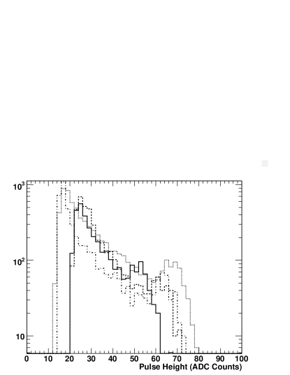
The pixel calibration has been studied using the 5.9 keV X-rays from a 55Fe source for various readout frequencies. Charge generated by X-rays which convert in the shallow depletion region near the pixel diode is fully collected, resulting in a pulse height peak corresponding to the full X-ray energy, or 1640 electrons. Pulse height spectra recorded on a single pixel for selected clusters are shown in Figure 1, for different readout frequencies.
The response to high momentum particles has been studied in beam tests. We used both the 1.3 GeV electron beam from the LBNL Advanced Light Source (ALS) booster and the 120 GeV secondary proton beam at the Meson Test Beam Facility (MTBF) at Fermilab, as part of the T966 beam test experiment. Data are converted into the lcio format, which is the persistency format adopted by the ILC studies. The data analysis is performed offline by a dedicated set of processors developed in the Marlin C++ framework. Events are first scanned for noisy pixels. The noise and pedestal values computed on-line are updated, using the algorithm in [2], to follow possible variations in the course of a data taking run.
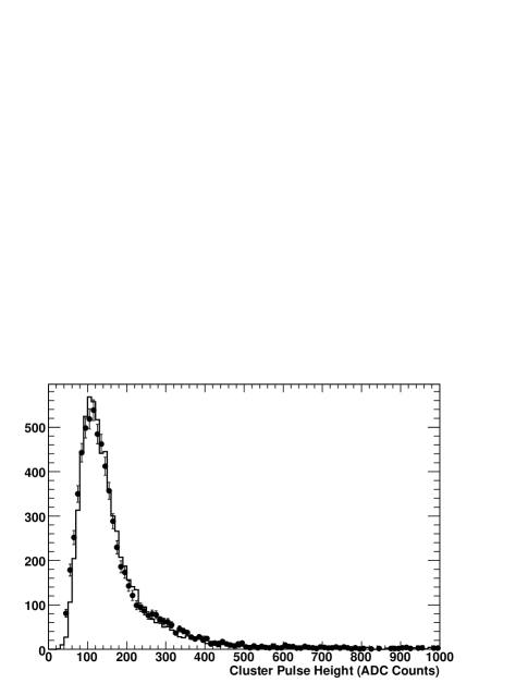
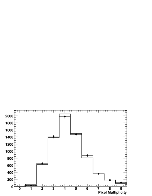
Cluster search is performed next. Each event is scanned for pixels with pulse height values over a signal-to-noise (S/N) threshold of 5, these are designated as cluster ‘seeds’. Seeds are then sorted according to their pulse heights and the surrounding, neighbouring pixels are tested for addition to the cluster. The neighbour search is performed on a 77 matrix surrounding the pixel seed and the neighbour threshold is set at 2.5, in units of the pixel noise. Clusters are not allowed to overlap, i.e. pixels already associated to one cluster are not considered for populating another cluster around a different seed. Finally, we require that clusters are not discontinuous, i.e. pixels associated to a cluster cannot be interleaved by any pixel below the neighbour threshold. The pixel response is simulated with a dedicated digitisation processor in Marlin [3]. The charge collection process is described starting from ionisation points generated along the particle trajectory using Geant 4 [4], by modelling the diffusion of charge carriers, originating in the epitaxial layer, to the collection diode. Simulated data are then processed through the cluster reconstruction stage, using the same processor as beam test data. A comparison of the real and simulated cluster pulse height and pixel multiplicity obtained, after simulation tuning, is shown in Figure 2
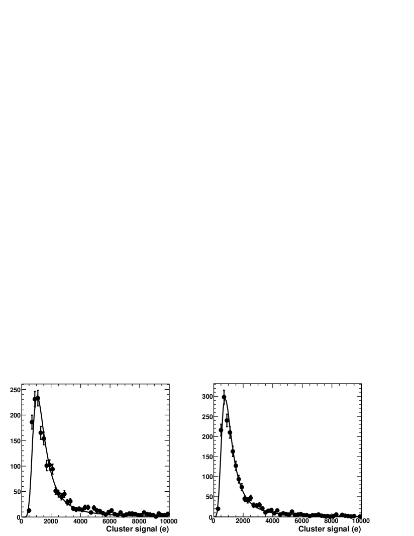
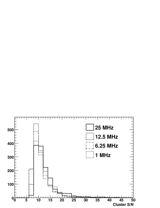
The most probable cluster pulse height for 120 GeV protons has been measured to be (111217) s for 5 m and (83013) s for 3 m collecting diodes as shown in Figure 3. The most probable pixel multiplicity scales from 2.7 to 4.3, respectively. An average signal-to-noise ratio of 12 to 13 has been measured for 1 MHz and 25 MHz readout, respectively (see Figure 4). The signal-to-noise performance is limited in part by the noise of the read-out board.
Finally, the response to low momentum electrons has been studied. The response of the detector to low energy electrons is important since particles from pair background have energies typically below 100 MeV. Data has been collected at the ALS with an Al beam scraper placed few meters upstream of the LDRD-2 detector. A large fraction of the registered hits are due to low energy electrons, originating from the interaction of the primary beam with the Al scraper, or to tertiaries, from photon conversions. These hits are characterised by large, asymmetric clusters, which suggest that low-energy background hits could be identified and rejected, based on the observed cluster shape.
III Conclusion
The LDRD-2 pixel cell, with small pitch and in-pixel charge storage for correlated double sampling, offers a viable architecture for a pixel chip with analog, fast readout, with potentially able to match the requirements for an ILC Vertex Tracker. Test chips have been characterised using 55Fe, an IR laser an particle beams. The chip performance is found to be stable up to the highest tested readout frequency of 25 MHz, corresponding to an integration time of 184 s. The pixel cell is the base of a chip of third-generation, which further addresses the ILC requirements. The LDRD-3 chip consists of a matrix of 9696 pixels on a 20 m pitch, with the same pixel cell as the LDRD-2. In addition, the chip features a column parallel readout at frequency up to 50 MHz and the digitisation performed on-chip, at the end of each column, by a row of successive approximation, fully differential ADCs featuring low power dissipation. Each ADC has a size of 20 m1 mm, which matches the pixel pitch. The digitisation of the 96 rows is performed in 1.9 s. The chip has been produced in AMS 0.35 m CMOS-OPTO process. Chips have been received back from the foundry in October 2007 and are currently being characterised.
References
- [1] M. Battaglia et al., In the Proceedings of International Symposium on Detector Development for Particle, Astroparticle and Synchrotron Radiation Experiments (SNIC 2006), Menlo Park, California, 3-6 Apr 2006, pp 0108.
- [2] V. Chabaud et al., Nucl. Instr. and Meth. in Phys. Res. A292 (1990), 75.
- [3] M. Battaglia, Nucl. Instr. and Meth,, A572 (2007) 274.
- [4] S. Agostinelli et al., Nucl. Instrum. Meth. A 506 (2003), 250.