Dependence of resistivity on surface profile in
nanoscale metal films and wires
Abstract
We extend quantum models of nanowire surface scattering to incorporate bulk resistivity and extract an expression for the increased resistivity due to surface roughness. To learn how to improve conductivity, we calculate conductivity degradation from individual wavelengths of surface roughness, and show how these can be convolved to give resistivity for arbitrary surfaces. We review measurements from Cu films and conclude that roughness at short wavelengths (less than 100 nm) dominates scattering, and that primarily specular scattering should be achievable for RMS roughness below about 0.7 nm.
As the minimum feature size in semiconductor technology continues to shrink, metal nanowires with thickness 45 nm are now needed to interconnect electronic nanodevices. However, measurements show nanowires have substantially higher resistivity than bulk metals Munoz ; GrainRefs , leading to interconnect delays, power loss, and other limits on performance. Scattering from surfaces, interfaces and grain boundaries are the causes of this conductivity degradation, but microscopic understanding of these effects and quantitative predictions of their magnitude have been limited. Here, we investigate the detailed dependence of conductivity on surface roughness profile and analyze the resulting technological impact.
The first quantitative treatments of surface and size effects in thin films or wires were the semiclassical methods of Fuchs Fuchs and Sondheimer Sondheimer . These approaches assume a ratio of carrier collisions with the surface reflect specularly, while scatter diffusely. Such theories can be fit to experiment with as a free parameter, but do not provide insight into how to improve conductivity.
More recently, surface roughness scattering has raised the attention of researchers in industry ChenGard ; Jiang ; Kapur , and quantum mechanical approaches to surface scattering calculations have been proposed. The two primary approaches include the Kubo linear response theory of Tes̆anović et al. Tesanovic and Trivedi and Ashcroft Trivedi , and the diagrammatic Keldysh formalism of Meyerovich and collaborators MeyerStep ; MeyerStep-bulk ; MeyerPon . Here we follow the approach of Meyerovich et al., which is readily applied to arbitrary surface roughness profiles. We calculate the contribution of each spatial frequency of surface roughness and convolve with roughness data extracted from experiments to gain insight into the nature of surface roughness scattering.
In our conductivity calculations, we consider a thin film because it reproduces the major qualitative results of a wire (and matches quantitatively when Eq. (9) below holds), while avoiding strong localization and other effects that make 1D systems problematic to deal with theoretically MeyerPon ; LeeRama . For the technologically important 10-100 nm scale, wire conductivity can be accurately estimated by combining effects of scattering from sidewalls to that from top and bottom surfaces.
In a thin film of thickness , boundary conditions at the surfaces lead to a density of states quantized in the transverse direction. As a result, the conduction band, described as the set of states at the Fermi energy, is broken into subbands with continuous parallel and quantized transverse components of the Bloch wavevector. Conduction states are then described by a subband index and a 2D wavevector , subject to the constraint that the total energy is equal to the Fermi energy:
| (1) |
(We treat the Fermi surface as effectively spherical, which is particularly appropriate for the best conducting metals, Ag, Cu, and Au). Even in a perfectly smooth film, this quantization leads to thickness-dependent conductivity, and to the quantum size effect (QSE), caused by the quantized dependence of the density of states on thickness Trivedi which is significant for very thin films (5nm).
Theoretical approaches to rough surfaces Tesanovic ; MeyerStep employ a (non-unitary) transformation to map the film with position-dependent surface into a flat film with bulk (non-Hermitian) perturbations. The scattering depends on the power spectral density (PSD) of the roughness, defined as the Fourier transformed surface height correlation function. In MeyerStep ; MeyerPon , a general isotropic 2D roughness power spectrum is treated with diagrammatic perturbation theory. By Fermi’s Golden Rule, the spatial frequencies of roughness determine the interband transition rates and hence a momentum loss rate matrix:
| (2) |
| (3) |
Here is the in-plane momentum satisfying (1) for subband , is the angle between initial and final carrier momentum, , and superscripts denote (2D) angular harmonics:
| (4) |
Surface roughness-limited conductivity is given by
| (5) |
where is resistivity, the scalar is the overall surface relaxation or mean free time, is carrier density, and is the overall surface momentum loss rate. Note that our definition differs from MeyerPon by an extra factor of because we use the usual 3D conductivity, as in Trivedi .
To combine bulk and surface scattering, we extend the method in Trivedi , adding momentum loss rates within subbands, to the case with interband transitions by adding matrices: . Since the primary bulk scattering mechanism at room temperature, acoustic phonons, is nearly isotropic Tomizawa , we use
with cm/s the Fermi velocity and = 39 nm the bulk mean free path for copper.
Adding matrices produces very different results from adding the scalars . Matthiessen’s rule, which states that for independent (series) resistivity mechanisms, breaks down in thin films when combining bulk and surface scattering MeyerStep-bulk ; Trivedi ; Munoz (Fig. 1 below). This breakdown can be understood because, absent bulk scattering, conductivity is dominated by carriers with momentum nearly parallel to the surface (low ) which rarely scatter from the surface. To consider surface scattering together with bulk scattering, we define
| (6) |
the effective surface roughness contribution to resistivity, which is independent of to first order 111 We can show by expanding in that ..
To study the effect of individual spatial frequencies of roughness on resistivity, we perform a first order functional expansion on . We define the first variation in with respect to the PSD component at wavevector with magnitude as the response to a special PSD:
| (7) |
Here is the response to a 2D PSD of the form
| (8) |
with the mean squared roughness of this PSD. The factor in (7) is necessary for consistent units.
Consistent with the validity of (2) – (5) to first order in roughness, we perform a first order functional expansion of in :
| (9) |
Here the LHS is the resistivity from an arbitrary 2D isotropic PSD , and in the RHS is given by Eq. (7).
The angular harmonics for (8) are given by
where is the Heaviside step function, and the delta function sets the angle between the initial and final wavevectors
Our results for the functional derivative (7) for surface-only scattering and effective rate with bulk scattering are plotted in Figure 1.
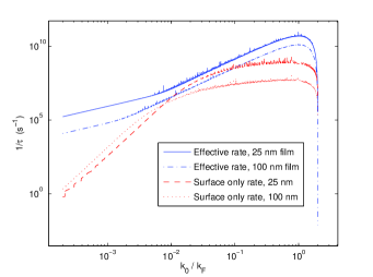
We tested the relation (9) for several PSDs, including our fit to experimental surface roughness data (see below). For the experimental fit, we find (9) holds to 2% for a 25 nm film and 1% for 100 nm. We conclude that, for films thick enough that , Eq. (9) provides an effective calculation of resistivities.
For larger values, which dominate surface scattering, the thickness dependence of the surface only resistivity is , as in MeyerPon ; Trivedi . But for large , we expect to approach the semiclassical result of Fuchs Fuchs and Sondheimer Sondheimer :
| (10) |
Fig. 1 indeed shows for most of the range.
For very small values, , while the surface-only rate actually increases with , . This can be explained by quantization. The subbands are spaced closest for lowest , so for , there is no scattering between higher order subbands. As becomes smaller, interband scattering due to surface roughness becomes impossible for lower and lower subbands. For , an increase in decreases the spacing between values, introducing interband transitions between low states where the spacing is smallest. Physically, this couples states traveling nearly parallel to the film surface with other states that interact much more strongly with the surface, providing a mechanism to increase with . For , in contrast, electrons in low states are already frequently scattered by bulk scattering. For small , only intraband scattering is possible, so there are always two final states and . At higher , the number of available final subbands becomes proportional to , so .
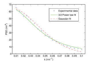
As can be seen from Fig. 1, spatial frequencies near (shortest wavelengths) have the strongest momentum loss, but the impact on conductivity depends on the actual roughness PSD of metal films and wires. Any attempts to improve conductivity will benefit from a knowledge of which components of surface roughness give the most improvement for the resources spent. Theoretical calculations often assume a Gaussian roughness spectrum, but experiments show that many PSD forms are present depending on the wire deposition conditions MeyerPon , and that real PSDs can fall of more slowly than Gaussian Feenstra . Unfortunately, the experimental literature on surface roughness spectra for metals is limited and focuses on relatively large length scales. Thus, we look to other materials. Feenstra et al. Feenstra observed that 1D STM scans of InAs/GaSb superlattice interfaces showed Lorentzian distributions,
For isotropic roughness, this corresponds to a 2D PSD of the form
| (11) |
with mean squared roughness . Eq. (11) also fits the AFM results of Moseler et al. Moseler for Cu films with , as shown in Fig. 2. Other experiments on copper films confirm a correlation length of 20 nm Keavney02 . We also fit Moseler ’s data to a Gaussian PSD, as shown in the figure. Because measurements at high spatial frequencies (which have a particularly strong effect on scattering) are lacking, our goal is to extrapolate from these fits 222Ref. Feenstra ’s STM of InAs/GaSb, which extends to wavevectors of 10 nm-1 compared to Moseler ’s AFM up to 0.1 nm-1, supports the fit in Eq. (11). Note that the flattening near the highest frequency is due to the finite sampling interval used in Moseler ..
We can use extrapolations from the Moseler data to calculate the resistivity, or equivalently the specular fraction . Substituting (9) in (10):
| (12) |
which (for 100 nm) is independent of . We find values of essentially 1 for the Gaussian PSD and () for Eq. (11). We get the same results when we use the full PSDs directly as in Eqs. (2) – (5)
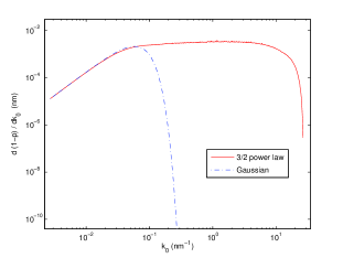
The fact that our analysis predicts highly specular () surface scattering for technologically-achievable surface roughness suggests that surface roughness scattering is a surmountable barrier to high conductivity. We can extract the most important components of roughness, taking into account both the relative strength of scattering and the observed roughness spectra. The effective diffuse scattering rate as a function of spatial frequency is shown in Fig. 3. More accurate measurements of the high frequency portion of the PSD are clearly needed, as the frequencies above 0.1 nm-1 are most critical to conductivity degradation.
Another way to understand these results is to note that for (11) with nm, = 90% corresponds to an RMS roughness of , compared to experimental measurements in the range 2 – 11 Å RMS-refs ; Purswani07 .
The experimental literature is somewhat mixed on the relative importance of surface scattering. Many results suggest that the observed resistivity increase is dominated by grain boundary rather than surface scattering GrainRefs , while some extract values of near 0 (diffuse rather than specular scattering) Purswani07 . As we have seen, depends strongly () on RMS roughness, which in turn depends on anneal times, deposition conditions, and other process variables. Another interesting explanation for this discrepancy may come from the experiment of Rossnagel et al. Rossnagel04 , who found that conductivity decreased strongly upon the deposition of an ultrathin Ta layer on top of a Cu film, but that the conductivity recovered when the Ta film was exposed to air, thereby oxidizing to become insulating. These observations suggest that thin barrier/adhesion layers rather than surface/interface roughness may be causing the apparent diffuse surface scattering.
To summarize, we have found that bulk scattering can be included in quantum models of surface scattering by adding matrices. This leads to violation of Mathiessen’s rule, but an effective surface resistivity independent of bulk scattering can be extracted. The resistivity from individual wavelengths of roughness can be convolved with roughness PSD to get for arbitrary surface. Our analysis suggests that roughness with wavelength within 1-2 orders of magnitude of the Fermi wavelength is the most critical for conductivity degradation.
We would like to thank K. Coffey and M. Moseler for providing experimental details, and R. Powell for useful discussions. This work was supported by Intel Corporation and the Semiconductor Research Corporation (SRC).
References
- (1) R. C. Munoz, C. Arenas, G. Kremer and L. Moraga, J. Phys.: Condens. Matter 15 (2003) L177-L184.
- (2) W. Steinhögl, G. Schindler, G. Steinlesberger, and M. Engelhardt, Phys. Rev. B 66 07514 (2002); J. W. C. De Vries, Thin Solid Films 167, 25 (1988); A. F. Mayadas, M. Shatzkes, and J. F. Janak, Appl. Phys. Lett. 14, 345 (1969); J. Appl. Phys. 39, 4241; Appl. Phys. Lett. 89, 114102; Phys. Rev. Lett. 54, 1840; J. Vac. Sci. Technol. 6, 690 (1969).
- (3) K. Fuchs, Proc. Cambridge Philos. Soc. 34, (1938) 100.
- (4) E. H. Sondheimer, Adv. Phys. 1 (1952) 1.
- (5) P. Kapur and J. P. McVittie, IEEE Trans. Electron Devices, 49 (2002) 590-604.
- (6) F. Chen and D. Gardner, IEEE Electron Device Lett., 19 (1998) 508-510.
- (7) Q.-T. Jiang, M.-H. Tsai, and R. H. Havemann, Interconnect Technology Conference, 2001. Proc. IEEE International, 227-229, 2001.
- (8) Z. Tes̆anović, M. V. Jaric and S. Maekawa, Phys. Rev. B 57 (1986) 2760-2763.
- (9) N. Trivedi and N. W. Ashcroft, Phys. Rev. B 35, (1987) 6435.
- (10) A. E. Meyerovich and A. Stepaniants, Phys. Rev. B 58 (1998) 13242.
- (11) A. E. Meyerovich and A. Stepaniants, J. Phys.: Condens. Matter 12 (2000) 5575.
- (12) A. E. Meyerovich and I. V. Ponomarev, Phys. Rev. B 65 (2002) 155413.
- (13) P. A. Lee and T. V. Ramakrishnan, Rev. Mod. Phys 57 (1985) 287.
- (14) J. Ziman, Electrons and Phonons (London: Oxford University Press) 452-460.
- (15) S. B. Soffer, J. Appl. Phys. 14 (1967) 1710.
- (16) S. B. Soffer, Phys. Rev. B 2 (1970) 3894.
- (17) S. F. Edwards and D. R. Wilkinson, Proc. R. Soc. Lond. A 381 (1982) 17-31.
- (18) R. M. Feenstra, D. A. Collins, D. Z.-Y. Ting, M. W. Wang, and T. C. McGill, Phys. Rev. Lett. 72 (1994) 2749.
- (19) M. Moseler, O. Rattunde, J. Mordiek, and H. Haberland. Comp. Mat. Sci. 10 (1998) 452-456.
- (20) K. Tomizawa, Numerical Simulation of Submicron Semiconductor Devices (Boston: Artech House)
- (21) D.J. Keavney, S. Park, and C.M. Falco, J. Appl. Phys. 91, 8108 (2002).
- (22) K. Coffey and K. Barmak, unpublished SRC Deliverable Report; K. Coffey, private correspondence.
- (23) J. Purswani and D. Gall, ICMCTF Proc. 2007 and refs. therein; W. Zhang, S. H. Brongersma et al., J. Appl. Phys. 101 063703 (2007).
- (24) S.M. Rossnagel and T.S. Kuan, J. Vac. Sci. Technol. B 22, 240 (2004).