Confined Ge–Pt states in self-organized Pt nanowire arrays on Ge(001)
Abstract
By means of band structure calculations within the density functional theory and the generalized gradient approximation, we investigate the electronic structure of self-organized Pt nanowires on the Ge(001) surface. In particular, we deal with a novel one-dimensional surface state confined in the nanowire array and clarify its origin. Due to large Pt contributions, the novel state is rather a mixed Ge–Pt hybrid state than a confined Ge surface state. Moreover, we compare our results to data from scanning tunneling microscopy.
pacs:
73.20.-r, 73.20.AtBecause of a wealth of extraordinary physical properties, self-organized nanowires recently attract great attention. Of special importance are self-organization phenomena on semiconductor surfaces, due to a wide field of possible technological applications. For the Ge(001) surface, for example, Au growth comes along with a large variety of ordering processes as a function of the Au coverage and growth temperature wang04 ; wang05 . Moreover, adsorption of Pt atoms results in well-ordered chain arrays after high-temperature annealing gurlu03 . These spontaneously formed Pt nanowires are promising with respect to their thermodynamical stablity, regularity, and length, which reaches up to several hundred nanometers. In order to obtain detailed insight into their physical properties and the self-organization process, exact knowledge about the surface electronic states is mandatory, which we address in the present paper.
A one-dimensional electronic state on the Pt-covered Ge(001) surface has been discovered by Oncel et al. oncel05 . Using scanning tunneling microscopy, the authors have measured spatial maps of the differential conductivity and afterwards calculated from these data the local density of states (DOS). At a temperature of 77 K and for a nanowire spacing of 1.6 nm, they find an unexpected DOS peak some eV above the Fermi level. They argue that this electronic state is located in the Ge trough between the Pt nanowires and, therefore, attribute it to a confined Ge surface state. However, the Ge(001) surface is known to be subject to strong hybridization under Pt coverage GePt . For this reason, we subsequently investigate the electronic structure of the Pt-covered Ge(001) surface by means of electronic structure calculations based on density functional theory. The band structure results discussed in the following rely on a fully relaxed supercell of the Ge–Pt surface, where the distance between neighbouring Pt nanowires has been set to 1.6 nm in order to prepare for a comparison of our first principles findings to the experimental DOS.

We use the generalized gradient approximation (GGA) implemented in the full-potential linearized augmented-plane-wave WIEN2k code wien2k , which is known for a very high capability in dealing with surfaces/interfaces GePt ; sur-int . The exchange-correlation potential here is parametrized according to the Perdew-Burke-Ernzerhof scheme. Our data is based on a supercell of the cubic Ge unit cell consisting of a reconstructed surface array and extending two unit cells perdendicular to the surface. The formation of Pt chains on Ge(001) is accompanied by the partial breakup of the Ge surface dimers gurlu03 . For obtaining a useful starting point for the structure optimization we thus start from the clean Ge surface, leave away each fourth row of upper Ge dimer sites, and place Pt atoms in the trough next to that row. Finally, we assume convergence of the structure optimization when the surface forces have decayed below a threshold of 5 mRyd/.

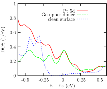
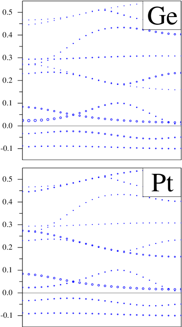
Fig. 1 shows partial Pt and Ge densities of states as resulting from our electronic structure calculation. As an example, we address the DOS of the upper dimer Ge site. However, the following discussion does not depend on this choice, as similar results are obtained for all Ge surface sites. For comparison, Fig. 1 includes the upper dimer Ge DOS for the clean Ge(001) surface without Pt nanowires Ge . Confirming the findings of Oncel et al. (oncel05, , Fig. 2b), for the Pt-covered surface a distinct structure appears in the Ge DOS just above the Fermi level, which we therefore ascribe to the novel electronic state under consideration. In the theoretical DOS, it is found at an energy of some eV, rather than at the experimental value of eV. Amazingly, the eV peak reappears in the Pt DOS with a very similar shape. While the Ge DOS in Fig. 1 is normalized with respect to the number of atoms contributing, the Pt DOS additionally has been downscaled by a factor 1/2. As a consequence, a significant amount of the spectral weight in the vicinity of the Fermi energy has to be attributed to the Pt nanowires. Furthermore, careful analysis of the band structure reveals that mainly two electronic bands of mixed orbital character give rise to the DOS structure around eV. Such a strong hybridization clearly points at significant Ge–Pt interaction. Fig. 2 depicts the band structure in the relevant energy range, where either the Ge or Pt contributions to the states are highlighted by means of the point size. The representation refers to the first Brillouin zone, and the direction parallel to the surface plane and perpendicular to the nanowires. A tiny band gap of approximately 0.03 eV is observed in fig. 2, reflecting the fact that the conductivitiy of the Pt-covered Ge(001) surface is basically connected to the nanowire formation.

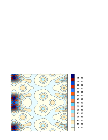
While the existence of a novel surface electronic state is confirmed, our band structure data spoil an interpretation in terms of a confined Ge surface state. Instead, as large Pt admixtures are due to strong Ge–Pt hybridization, the state must originate from both the Ge surface and the Pt nanowires. Supporting our line of reasoning, scanning tunneling microscopy (STM) data, as obtained by Schäfer et al. schafer06 , show that the Pt conduction bands are seriously modified by the interaction with the Ge substrate. For comparison, we present a simulted STM image in fig. 3. The image indicates a remarkable dimerization of the Pt valence states, which are seen in the very center of fig. 3, running from top to bottom. However, contradicting the experiment, this dimerization does not vanish for states close to the Fermi level. Modelling the surface energy levels in terms of a quantum mechanical particle in a well, as proposed in oncel05 , does not suffer from our interpretation in terms of mixed Ge–Pt states. Exactly the same applies to the fact that the state gradually fades away close to structural defects of the nanowires or the substrate. In contrast, the experimental observation of an almost perfect localization within the Ge trough is puzzeling because of the large Pt admixtures. However, the simple shape of the band with the largest Ge–Pt hybridization in fig. 2 indicates that the novel surface state is captured by the classical Kronig–Penney model. Thus, it is well described in terms of a non-localized Ge–Pt state confined in the periodic potential of the nanowire array.
In conclusion, we have presented first principles band structure calculations for the Pt-covered Ge(001) surface and studied the surface electronic structure. In particular, we have focussed on a novel electronic state, located right above the Fermi energy, which is not found for the clean Ge(001) surface. Contradicting a previous experimental prediction, our data show that this state does not originate from simple confinement of a regular Ge surface state. For an adequate interpretation of the experimental DOS it is essential to account for strong Ge–Pt hybridization, which is not surprising because interaction between the substrate and the adsorbate is expected to be of great importance for the adsorption process GePt ; schmitt05 .
Financial support by the Deutsche Forschungsgemeinschaft (SFB 484) is acknowledged.
References
- (1) J. Wang, M. Li, and E.I. Altman, Phys. Rev. B 70, 233312 (2004).
- (2) J. Wang, M. Li, and E.I. Altman, Surf. Sci. 596, 126 (2005).
- (3) O. Gurlu, O.A.O. Adam, H.J.W. Zandvliet, and B. Poelsema, Appl. Phys. Lett. 83, 4610 (2003).
- (4) N. Oncel, A. van Houselt, J. Huijben, A.-S. Hallbäck, O. Gurlu, H.J.W. Zandvliet, and B. Poelsema, Phys. Rev. Lett. 95, 116801 (2005).
- (5) U. Schwingenschlögl and C. Schuster, Europhys. Lett. 81, 26001 (2008).
- (6) U. Schwingenschlögl and C. Schuster, Chem. Phys. Lett. 439, 143 (2007); Appl. Phys. Lett. 90, 192502 (2007); Europhys. Lett. 81, 17007 (2008).
- (7) P. Blaha, K. Schwarz, G. Madsen, D. Kvasicka, and J. Luitz, WIEN2k: An augmented plane wave and local orbitals program for calculating crystal properties (Vienna University of Technology, Austria, 2001).
- (8) U. Schwingenschlögl and C. Schuster, Chem. Phys. Lett., 449 126 (2007).
- (9) J. Schäfer, D. Schrupp, M. Preisinger, and R. Claessen, Phys. Rev. B 74, 041404(R) (2006).
- (10) T. Schmitt, A. Augustsson, J. Nordgren, L.-C. Duda, J. Höwing, T. Gustafsson, U. Schwingenschlögl, and V. Eyert, Appl. Phys. Lett. 86, 064101 (2005).