In situ x-ray diffraction study of epitaxial growth of ordered Fe3Si films
Abstract
Molecular beam epitaxy of Fe3Si on GaAs(001) is studied in situ by grazing incidence x-ray diffraction. Layer-by-layer growth of Fe3Si films is observed at a low growth rate and substrate temperatures near 200 ∘C. A damping of x-ray intensity oscillations due to a gradual surface roughening during growth is found. The corresponding sequence of coverages of the different terrace levels is obtained. The after-deposition surface recovery is very slow. Annealing at 310 ∘C combined with the deposition of one monolayer of Fe3Si restores the surface to high perfection and minimal roughness. Our stoichiometric films possess long-range order and a high quality heteroepitaxial interface.
pacs:
81.15.Hi, 61.10.Nz, 68.35.Bs, 75.50 CcCombinations of magnetic and semiconducting materials lead to further development in the field of magnetoelectronics Prinz (1996); Parkin et al. (2004). Ferromagnet/semiconductor heterostructures should possess a rather perfect interface Hashemifar et al. (2005) to minimize the scattering of spins. High thermal stability is required for device processing and operation. Fe3Si on GaAs is a promising candidate for magnetoelectronic applications Hong et al. (1991); Liou et al. (1993); Ionescu et al. (2005). The Curie temperature of Fe3Si is as high as 567 ∘C Nakamura (1988) and the Fe3Si / GaAs interface is stable up to more than 400 ∘C Herfort et al. (2005). Spin injection through the Fe3Si / GaAs interface at room temperature has been demonstrated recently Kawaharazuka et al. (2004). The lattice misfit between stoichiometric Fe3Si and GaAs is very small Herfort et al. (2003, 2006) and allows for the formation of a perfect interface without strain releasing defects like misfit dislocations. The lattice match and the long range order of the as-grown thin epitaxial films depend on the stoichiometry Jenichen et al. (2005). Significant changes of the saturation magnetization and the sheet resistance with film stoichiometry have been observed Herfort et al. (2004).
The layer-by-layer growth mode allows for well controlled fabrication of epitaxial layer sequences with very sharp interfaces between them. The aim of the present work is the in situ characterization of the Fe3Si epitaxial growth process in the layer-by-layer growth mode by x-ray surface diffraction methods. The surface and interface roughness and long range order in the films are monitored under ultrahigh vacuum conditions. We use grazing incidence x-ray diffraction (GID) which is ideally suited for thin film investigations. Fe3Si films can be grown by molecular beam epitaxy (MBE) at GaAs substrate temperatures near 200 ∘C Herfort et al. (2003). They were grown for the present study in an MBE chamber inserted onto the diffractometer at the wiggler beamline U125/2 KMC Jenichen et al. (2003) at the storage ring BESSY in Berlin. A double crystal Si(111) monochromator was used. The energy of the radiation was 10 keV and the incidence angle was kept at 0.3 ∘. The acceptance angle of the detector was 0.1 ∘ both perpendicular and parallel to the surface.
GaAs(001) templates were prepared in a separate III-V growth chamber using standard GaAs growth techniques. The sample was then capped by As and transferred into the MBE system at BESSY for the Fe3Si deposition by means of an ultrahigh vacuum shuttle. The As cap was removed by annealing the sample in the preparation chamber at a temperature of 350∘C before transferring it into the growth chamber. The Fe3Si layers were then grown on the As-rich c() reconstructed GaAs surface at different substrate temperatures near 200∘C with a growth rate of 3 monolayers (ML) per hour, similar to the procedure described in Ref. Herfort et al., 2003 (1 ML nm, where is the lattice parameter). The Si and Fe cell temperatures were tuned in order to obtain a perfect lattice match of the films. The position of the Fe3Si layer peak of the x-ray diffraction curve was monitored in order to reach a coincidence with the corresponding GaAs peak. We obtained optimum temperatures of 1239∘C and 1370∘C for the Fe and the Si cells, respectively.
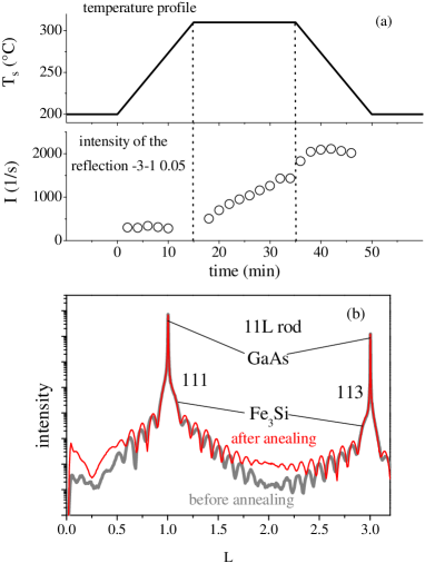
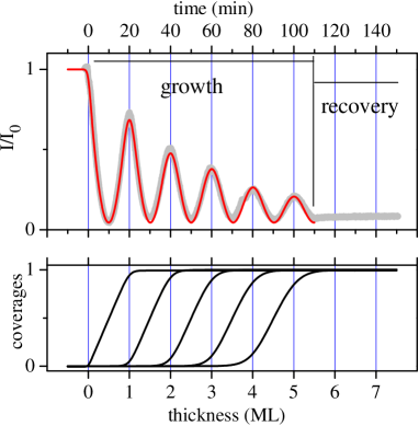
Layer-by-layer growth is observed by x-ray intensity oscillations during deposition of Fe3Si, Fig. 1 (a). The x-ray intensity is measured in the reciprocal space point 1 1 0.05, close the bulk forbidden reflection 1 1 0. The oscillations are continuously damped, indicating gradual surface roughening. The oscillation period is s. Such a low growth rate facilitates the formation of a highly ordered Fe3Si film. Recovery of the diffracted intensity after growth is very slow. In order to overcome this slow recovery and restore the initial flat surface, the surface was annealed at 310∘C for about 20 min with simultaneous deposition of one monolayer of Fe3Si. This procedure considerably improves the flatness of the Fe3Si surface, as observed by the increase of the intensity of bulk forbidden surface sensitive reflections by a factor of about ten, see Fig. 2 (a). The same annealing procedure was also used for surface preparation before the measurement shown in Fig. 1 (a).
Crystal truncation rods (CTRs) presented in Fig. 2 (b) demonstrate the results of growth and the effect of annealing in more detail. A nearly perfect angular coincidence of the Fe3Si and GaAs peaks is achieved by the fine tuning of the Fe and Si cell temperatures. An almost perfect lattice match of the films during and after growth is attained. The Fe3Si peaks are broader and less intense due to small thickness of the film. The shape of the CTRs in the middle between bulk diffraction peaks is a measure of the surface roughness Robinson (1986). High intensity indicates a well-ordered, highly planar surface. The intensity of the 1 1 L rod in Fig. 2 (b) in the vicinity of the bulk forbidden reflections 1 1 0 and 1 1 2 increase by an order of magnitude during annealing. Thus, the original high quality of the surface can be restored by the annealing cycle. Pronounced thickness fringes observed on the CTR imply smooth and parallel top and bottom interfaces. These fringes evidence not only a smooth surface but also a a high quality of the Fe3Si / GaAs interface Jenichen et al. (2007). We checked this by means of simulation of the corresponding x-ray reflectivity curves.
The kinematical diffraction theory from stepped surfaces Cohen et al. (1989) describes the average surface shape during growth in terms of coverages of successive levels. In the ideal case, growth starts (at ) from a perfectly flat surface with and for ( is integer). During growth, the coverages run from 0 to 1 with , Fig. 1 (b). Two successive terrace levels interfere completely destructively under the antiphase diffraction condition. For the zinc blende structure, this condition is met for reflections with odd at , i.e., for simultaneously grazing incidence and grazing exit diffraction conditions Braun et al. (2003). The destructive interference at originates from the lateral shift of the successive crystalline layers in the zinc blende structure, which accompanies the vertical shift.
The diffracted intensity at the antiphase condition is proportional to the interference function
| (1) |
where is the structure amplitude of the given reflection and is the exposed coverage on the th level of the surface Cohen et al. (1989). The time dependence of the layer coverage can be described by the continuity equation
| (2) |
where is the time required for the deposition of one monolayer. For ideal layer-by-layer growth, the fluxes are the Heaviside step functions, . An imperfect layer-by-layer growth can be described by the smoothed functions Braun et al. (2003)
| (3) |
The changes in the onset and completion of the formation of subsequent monolayers can be modeled by choosing appropriate widths . We assume according to Ref. Braun et al. (2003), a power law dependence, . The layer coverages shown in Fig. 1 (b) are obtained from a fit to measured growth oscillations with the parameters and . Figure 1 (b) presents the resulting time dependence of the coverages.
Intensities of the Fe3Si reflections depend on the long-range order of the atoms in the sublattices. Fe3Si has the face centered cubic D03 structure that can be viewed as a fcc lattice with the basis consisting of four atoms A, B, C, and D with coordinates A(0, 0, 0), B(0.25, 0.25, 0.25), C(0.5, 0.5, 0.5), and D(0.75, 0.75, 0.75) Niculescu et al. (1976); Hines et al. (1976); Jenichen et al. (2005). In the ordered Fe3Si crystal, Fe atoms occupy three sublattices A, B, and C, while Si atoms take the sublattice D. The disorder is described by two order parameters and , which are fractions of Si atoms occupying the Fe(B) and Fe(A,C) sites, respectively. The reflections from a partially disordered crystal can be divided into three types, fundamental reflections and two types of superlattice reflections. Fundamental reflections, that are not influenced by disorder, are given by , where is an integer. The structure amplitude of such reflections is
| (4) |
where and are atomic scattering factors of the respective elements. Reflections with odd are sensitive to both types of disorder, the structure amplitude being
| (5) |
Reflections given by are sensitive to disorder in the Fe(A,C) sublattice,
| (6) |
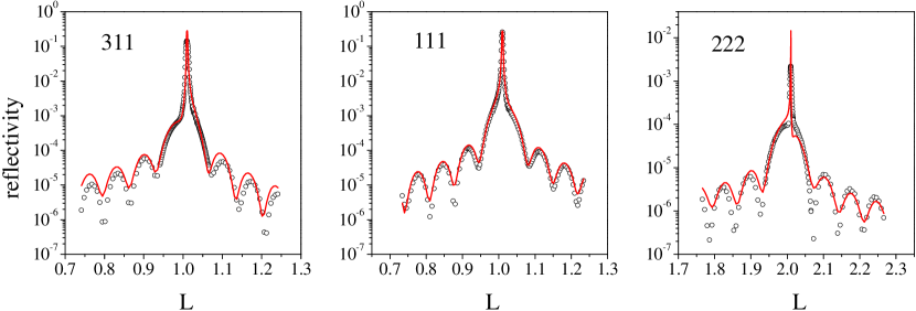
Figure 3 compares measured and calculated x-ray diffraction curves for the reflections that are sensitive to different types of disorder: 1 1 1 and 3 1 1 reflections are sensitive to disorder in both sublattices, see Eq. 5, while the 2 2 2 reflection is sensitive to disorder in the Fe(A,C) sublattice, see Eq. 6. The x-ray intensity distribution along each CTR was calculated as a sum of the amplitudes for two-beam dynamical diffraction problems corresponding to different reciprocal lattice points along the given CTR Kaganer (2007). 16 reflections were included in the sum. The Fe3Si film thickness obtained from the intensity calculations is 29 ML. The calculations are performed for a fully ordered film, . The experimental curves were scaled to the calculated ones by requiring equal integrated intensities of the substrate peaks. With this scaling, the intensities of the Fe3Si peaks reach the theoretical values, thus proving the full order of the film. Similar results were obtained for other lattice matched films grown at low growth rate. In conclusion, we have found the layer-by-layer growth conditions during MBE of Fe3Si films on GaAs (001) substrates at low growth rates ( 3 ML/h) and performed in situ experiments using grazing incidence x-ray diffraction. An excellent surface and interface quality was achieved. The growth of lattice matched films at such a low rate leads to a high degree of long-range order. The authors thank Claudia Herrmann, Steffen Behnke, Hans-Peter Schönherr and Tatsuro Watahiki for support during the experiments, and Uwe Jahn and Achim Trampert for critical reading of the manuscript.
References
- Prinz (1996) G. A. Prinz, Science 54, 17638 (1996).
- Parkin et al. (2004) S. P. Parkin, C. Kaiser, A. Panchula, P. Rice, B. Hughes, M. Samant, and S. H. Yang, Nature Mat. 3, 862 (2004).
- Hashemifar et al. (2005) S. J. Hashemifar, P. Kratzer, and M. Scheffler, Phys. Rev. Lett. 94, 096402 (2005).
- Hong et al. (1991) M. Hong, H. S. Chen, J. Kwo, A. R. Kortan, J. P. Mannaerts, B. E. Weir, and L. C. Feldman, J. Cryst. Growth 111, 984 (1991).
- Liou et al. (1993) S. H. Liou, S. S. Malhotra, J. X. Shen, M. Hong, J. Kwo, H. S. Chen, and J. P. Mannaerts, J. Appl. Phys. 73, 6766 (1993).
- Ionescu et al. (2005) A. Ionescu, C. A. F. Waz, T. Trypiniotis, C. M. Gürtler, H. Garcia-Miquel, J. A. C. Bland, M. E. Vickers, R. M. Dalgliesh, C. Langridge, Y. Bugoslavsky, et al., Phys. Rev. B 71, 094401 (2005).
- Nakamura (1988) Y. Nakamura, Landolt-Börnstein New Series III/19c (Springer, Berlin, Germany, 1988), chap. 1, p. 26.
- Herfort et al. (2005) J. Herfort, H.-P. Schönherr, A. Kawaharazuka, M. Ramsteiner, and K. H. Ploog, J. Cryst. Growth 278, 666 (2005).
- Kawaharazuka et al. (2004) A. Kawaharazuka, M. Ramsteiner, J. Herfort, H.-P. Schönherr, H. Kostial, and K. H. Ploog, Appl. Phys. Lett. 85, 3492 (2004).
- Herfort et al. (2003) J. Herfort, H.-P. Schönherr, and K. H. Ploog, Appl. Phys. Lett. 83, 3912 (2003).
- Herfort et al. (2006) J. Herfort, B. Jenichen, V. Kaganer, A. Trampert, H.-P. Schönherr, and K. H. Ploog, Physica E 32, 371 (2006).
- Jenichen et al. (2005) B. Jenichen, V. M. Kaganer, J. Herfort, D. K. Satapathy, H. P. Schönherr, W. Braun, and K. H. Ploog, Phys. Rev. B 72, 075329 (2005).
- Herfort et al. (2004) J. Herfort, H.-P. Schönherr, K.-J. Friedland, and K. H. Ploog, J. Vac. Sci. Technol. B 22, 2073 (2004).
- Jenichen et al. (2003) B. Jenichen, W. Braun, V. M. Kaganer, A. G. Shtukenberg, L. Däweritz, C. G. Schulz, and K. H. Ploog, Rev. Sci. Instr. 74, 1267 (2003).
- Robinson (1986) I. K. Robinson, Phys. Rev. B 33, 3830 (1986).
- Jenichen et al. (2007) B. Jenichen, V. M. Kaganer, W. Braun, J. Herfort, R. Shayduk, and K. H. Ploog, Thin Solid Films 515, 5611 (2007).
- Cohen et al. (1989) P. I. Cohen, G. Petrich, P. R. Pukite, and G. Whaley, Surface Science 216, 222 (1989).
- Braun et al. (2003) W. Braun, B. Jenichen, V. M. Kaganer, A. Shtukenberg, L. Däweritz, and K. H. Ploog, Surface Science 525, 126 (2003).
- Niculescu et al. (1976) V. Niculescu, K. Raj, J. I. Budnick, T. J. Burch, W. A. Hines, and A. H. Menotti, Phys. Rev. B 14, 4160 (1976).
- Hines et al. (1976) W. A. Hines, A. H. Menotti, J. I. Budnick, T. J. Burch, T. Litrenta, V. Niculescu, and K. Raj, Phys. Rev. B 13, 4060 (1976).
- Kaganer (2007) V. M. Kaganer, Phys. Rev. B 75, 245425 (2007).