Anomaly in Andreev reflection at large ferromagnet/high-TC superconductor area junctions with rough interface
Abstract
Sub-gap conductance at a large area junction with a rough interface of a ferromagnet and a high-TC superconductor is superimposed by multiple peaks which is not expected from an ideal point contact Andreev reflection process. We demonstrate this phenomenon by measuring resistance as a function of bias voltage of a Co/Y1Ba2Cu3O7-δ junction with contact area 50 x 70 at various temperatures. In order to analyze such Andreev reflection data, the interface is assumed to have random potentials which can create local electric fields. The Blonder-Tinkham-Klapwijk theory is modified with the inclusion of a broadening parameter due to finite life time effects of quasi particles. An additional voltage drop due to local electric fields at the rough interface has been included in terms of an extra energy shift which may be related to the asymmetry of normalized resistance data. Spin polarization has been introduced for the ferromagnet. The presented model explains the multi-peak nature and asymmetry of Andreev reflection data experimentally observed at large area junctions. Extension of the model also interprets the experimentally observed anomalous enhancement of resistance peaks in the sub-gap region which may result from crossing the critical current limit across the junction.
pacs:
75.50.Pp, 72.25.Dc,72.25.Mk,74.45.+cI Introduction
Andreev reflection (AR) is a process that converts quasi-particle currents in a normal metal (N) to supercurrents in a superconductor (SC) at a N/SC- interface. Only a single electron in N with energy (E) smaller than the superconducting gap () can get into the SC by pairing up with an electron of opposite momentum and spin. This is accomplished by the reflection of a hole back
into the metal, a process first described by Andreev.af AR results in an enhancement of the N/SC junction conductance beyond its normal state value in the sub-gap region. The theoretical explanation of AR was given by Blonder, Tinkham and Klapwijk in 1982.BTK When N is replaced by a ferromagnet (FM), AR at the FM/SC interface is suppressed due to the spin imbalance leading to a decrease of the sub-gap conductance. A measurement of this suppression yields the magnitude of spin polarization () in the FM.soulen ; upa In order to incorporate spin polarization in the modelling, Strijkers . introduced a method of subdividing the total current across the interface into a polarized and an unpolarized part.Strijker The determination of by modelling AR spectroscopic data is strongly dependent on the interface quality of the FM/SC junction. The Blonder-Tinkham-Klapwijk (BTK) theory describes the interface as a delta function potential.BTK This is a simple description and it can not describe AR at rough large area junctions. Hence, modification is necessary in order to explain realistic experimental AR data.
Depending on the interface quality, the junction resistance also varies. Classical junctions of macroscopic size are governed by Maxwell resistance () for a small contact area of radius with the mean free path and the specific resistivity of a metal, . Ballistic point contacts are defined in a semi-classical description for and are governed by Sharvin resistance . Wexler’s formula relates Maxwell and Sharvin resistance by , where is a slowly varying function. Essentially, the BTK theory is applicable to ballistic point contacts and s-wave superconductors.
A tunneling theory for normal metal-insulator--wave
superconductors has been reported by Tanaka and Kashiwaya.tana_kashi However, it has been shown by Barash Barash that the character of the change in the order
parameter at the junction of a -wave superconductor and
normal metal is not much different from a junction with
a -wave superconductor when the orientation of the normal metal to
the -wave superconductor is along the principal crystallographic axes. It implies that AR at
a junction of N and -wave SC with junction normal along a principal crystallographic axes of -wave SC is similar to AR at the isotropic N/s-wave SC junction. For example, a recent AR study reveals that when a thin Y(YBCO) film, a high-TC superconductor, is oriented
with the c-axis normal to the interface, a zero bias conductance peak is observed.luo These results evidence
that the problem of anisotropy in the order parameter can be solved by studying FM/high-TC SC junctions along a principal crystallographic axes. However, the interface roughness is difficult to be avoided. For example, it is reported that YBCO films grow with
large-angle grain boundaries and obstruct the development of reproducible Josephson junctions of different types.alex Droplet formation on YBCO thin films grown by pulsed laser deposition is a known feature mozhaev and an unavoidable source of noise which occurs during conductance measurements across FM/YBCO junctions. The interface can never be smooth and homogeneous,if a normal or ferromagnetic material is deposited on an amorphous superconductor like tungsten carbide ralph . The roughness of surface has already been taken into account to do quantitative fitting of AR data in high-TC SC.Fogel Hence, it is necessary for us to consider the influence of interface scattering and roughness when modelling real AR thereby modifying initial BTK formula.
Additionally, when the current across the FM/high-TC SC junction reaches locally the critical current () for the superconductor at any bias (eV), the superconductor becomes a normal metal. For a fixed bias the critical current may be locally reached at a rough FM/SC junction yielding an increase of resistance where the superconductivity is lost, thus causing additional noise in the differential resistance measurement.goutam ; hind As a result, AR data are superimposed by heavy noise, when AR measurements are carried out on rough FM/SC junctions. In general, noise is a time dependent phenomenon. However, in the present case, noise refers to the multi-peak nature of differential resistance data as a function of bias voltage. We extend the original BTK model in order to explain the anomalous increase of resistance caused by critical current effects also.
In this paper, we report on the AR experiments and modelling of AR data across FM/high-TC SC junctions grown along the (001) crystallographic direction. The motivation is to identify the problems in Andreev reflection usually occurs in large area FM/high-TC junction and to try to explain them in the light of modified BTK modelling. We have dealt mainly with the problems faced during the AR experiments with FM/high-TC SC samples. Efforts have been made to theoretically model those AR data with help of the relatively new idea of multi-point contacts. Since surface roughness is inevitable for high-TC SC like YBCO, we believe large N-metal/YBCO junction would be the right candidate for invoking this new concept. In addition, we chose FM-metal/YBCO junction in order to show that we can extract information about spin polarization of FM by modeling AR with multi-point contacts.
We demonstrate the occurrence of anomalous multi-peaks in AR data by carrying out resistance measurements as a function of bias voltage for Co/YBCO samples with 50x70 m2 contact area. We will show how the interface roughness influences the shift of the resistance dip away from zero bias. Our model is capable of determining the of Co and the of YBCO. Furthermore, we will discuss the additional enhancement of resistance due to the influence of critical current (Sect. 4.1).
II Theory
II.1 Ideal Andreev reflection
The BTK model employs a generalized semiconductor scheme to match the wavefunctions at the N/SC interface with some specific boundary conditions. The system we consider is described by Bogoliubov-de-Gennes matrix equations for electrons and holes which are coupled. Because the point contact is assumed to be along a crystallographic axis, the model may be restricted to one dimension in the present case of small contact area. The repulsive potential H (x) models the elastic scattering that usually occurs in the orifice at the N/SC interface. The diameter and the width of the interface should be less than the mean free path of N and the coherence length of SC. The interface barrier strength is varied through a parameter = H/( vF), where vF is the Fermi velocity. According to BTK theory, the current (INS) across a N/SC junction can be described as,
| (1) |
where
and, e=electronic charge, N = BCS density of states, vF = Fermi velocity, = junction
cross sectional area, f0 = Fermi distribution function, V =
applied voltage, A(E)= probability of Andreev reflection and B(E)=
probability of normal reflection. Temperature effects are included via vF and f0.
It is well known that Cooper pairs of the superconductor layer usually get diffused into the metal and a weakly superconducting layer is created in the metallic side of the junction. This is called proximity effect.
On the microscopic level, the proximity effect is completely described by the Andreev reflection process.
This superconducting proximity layer has a lower transition temperature and a lower than the bulk superconductor. The AR occurs
at the metal/proximity-layer interface and it is limited to bias voltages smaller than the superconducting gap value () of the proximity layer. However, quasiparticles can only enter the SC for voltages higher than the bulk gap().
Hence, there are two gap parameters to be incorporated into the fitting procedure, one for Andreev reflection and proximity effect , the other for quasiparticle transport .Strijker We have observed that the modelled is always smaller than .
II.2 Effect of spin polarization
The BTK theory is valid for AR at a N/SC junction. This model does not give information about spin polarization when the metal is ferromagnetic. In order to account for the influence of on AR, we have to consider that when a spin-up polarized electron is incident at the junction, it needs another spin-down polarized electron to get into the SC. Because a Cooper pair in the superconductor is composed of a spin-up and a spin-down electron, the removal of the spin-down electron leaves a spin-up hole which is Andreev reflected back into the metal. Since, the spin-up hole is considered as the absence of a spin-down electron and so by convention it should be in the spin-down density of states (DOS).soulen The magnitude of AR changes in dependence on the availability of spin-down electronic states. For example, there will be no spin-down electronic states for a 100 spin polarized material and AR is not observed. The effect of can be taken into account by separating the total current INS across the junction into polarized IP and unpolarized IU parts. Strijker We have substituted the expression of INS from Eq. 1 for IU and IP, differentiated INS with respect to voltage as given below and then numerically integrated on energy scale.
| (2) |
where
II.3 Influence of interface scattering
Because the modelled conductance peaks are sharp and do not match the broad experimental conductance, sometimes it is not sufficient to model AR data with the parameters, , , , and . Here, we take into consideration broadening of peaks by including a complex part in the energy as according to P. Szabo where large scattering at the interface and finite life time effects are taken into account by .Szabo This broadening parameter has been proposed Dynes and employed by several authors before. Srikanth The BCS density of states in Eq. 1 ( is modified to (]) when the lifetime broadening parameter is included. It should be mentioned that the BTK model is restricted to one dimension. On a scale shorter than the coherence length , the energy gap () rises to its asymptotic value and the evanescent waves also decay.BTK In the case of high-Tc superconductors most likely this is violated due to extremely short coherence lengths. Moreover, the existence of a thin native non-superconducting layer on YBCO due to surface degradation has been probed by tunneling measurements.Iguchi This gives rise to inelastic scattering to the incoming electrons. Usually, such normal state scattering destroys the quantum phase coherence of the carriers crossing the junction and the modification of BTK model incorporating finite life time broadening is quite relevant. Hence, the inclusion of an imaginary term in the energy is an effective technique to describe life time effects in tunneling and it is reasonable to do the same in the BTK framework also. The modelling with five parameters, , (, ), and , is quite useful for sub-gap conductance data probed on FM/SC junctions. The interface scattering can be efficiently taken into account by the parameter.
III Experiments
YBCO films have been deposited by pulsed laser deposition on sapphire substrates in oxygenated atmoshphere.lorenz The Co/YBCO heterostructure has been prepared by thermal evaporation of Co on YBCO under a vacuum level of 3 x 10⁻³ mbar. Actually, the Co deposition was carried out on YBCO surface in ex-situ condition. Since, YBCO surface was exposed in air before, the oxygen atoms have been adsorbed at apical cites as described by M. Naito.naito If the Co took oxygen from the YBCO surface, it would have taken only the adsorbed oxygen. Hence, it is expected that ex-situ process provided fairly good junction in Co/YBCO. However, if it happens to have oxygen deficient surface of YBCO due to Co deposition, that may help in obtaining longer coherence length. Because, it has been reported that coherence length of YBCO increases with oxygen deficiency.ossa We have prepared samples with 50 x 70 m2 contact area by photo-lithography and selective area etching. The samples are made in a cross geometry. The measuring electrodes are fabricated by depositing silver contacts on the contact pads. Two contacts are made on Co pads, while the other two contacts are made on YBCO pads. The resistance vs applied bias voltage measurement has been carried out by AC modulation technique using a lock-in amplifier in a continuous flow cryostat from 10 to 100 K. The applied frequency is 11 Hz. It has been observed that the critical current density of YBCO has not been changed after deposition of Co.ng The junction resistance lies in the M range at room temperature and it can be in tunneling limit.The reason of high resistance can be the rough interface of YBCO itself. Another possibility may be the formation of Cobalt oxide layer between YBCO and Co. Hence, we could not observe clear Andreev reflection. Nevertheless, we have observed some abnormalities in AR and tried to explain them with the help of modified BTK theory in the following sections.
IV Results and Discussion
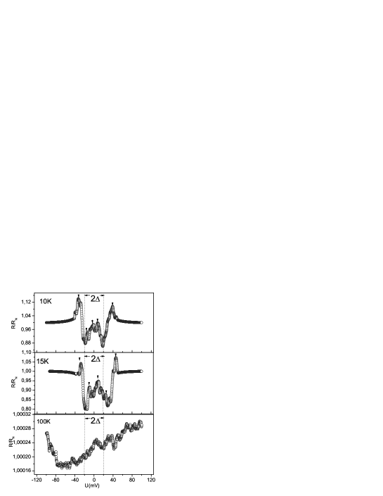
We have observed resistance variation at Co/YBCO with 50 x 70 m2 contact areas at low temperatures within the superconducting gap ( = 20 meV) of YBCO. The measured normalized resistance at 10, 15 and 100 K are presented in Figure 1. It is noticed that a particular feature of the measured voltage with in the superconducting gap (Figure 1(a) and (b)) is not present at 100 K (Fig. 1(c)). Our study suggests that this feature has been caused due to AR. However, even at 10-15 K the signature of AR is superimposed by multi-peaks possibly due to the high junction resistance and large rough interface area.
In this regard, it has to be mentioned that, we have not observed multi-peaks in AR for Co/YBCO samples of much smaller contact area. The modified BTK modelling of the normalized resistance data of those samples reports a spin polarization of Co around 34.ng
In order to explain the origin of multi-peaks in normalized resistance data of Co/YBCO with 50 x 70 m2 contact areas, we can proceed in the following way.
It is assumed that a rough, large N/SC interface can be divided into several point contacts with different barrier heights and scattering rate .
The barriers are distributed in space. Every barrier corresponds to one point contact whose dimension should be less than the mean free path of the FM and coherence length of SC.
When the contact area is large, a shift of the zero bias resistance (ZBR) dip in the differential resistance data can also occur.
In principle, the assumption of a delta function potential barrier across N/SC junction in BTK model only applies for ideal junctions. For example, the roughness of real FM/high TC junctions can be taken into account by randomly distributed potential barriers at the interface. These are uncorrelated random potentials which can result into local electric fields at the junction.
The effect of electric field on ballistic transport of quasiparticles in mesoscopic system has already been analyzed theoretically. It is reported that a peak can develop in AR conductance as a function of biased voltage and it can change sign when the direction of electric field is changed.Mina
A local electric field can alter the distribution of energy levels, which may change the density of states of quasi particles at the Fermi level. As a result, one can observe asymmetry in the normalized conductance vs voltage plot since this plot usually follows the density of states.
Hence, an additional voltage drop has been introduced in terms of an extra energy loss in the expression of AR probability to account for the influence of local electric field.
This extra energy can be related to a shift of ZBR dip in real experiments.
Thus, we can assume that when a current passes through a single point contact at a real junction with rough, large interface, an additional voltage drop depending on the magnitude of such local field may occur which can be represented by an extra energy . The current vs voltage characteristics have been numerically calculated with an additional energy loss and are represented in Figure 2(a).
Different slopes are recognized inside and outside the superconducting gap (20 meV). The slope change around 20 mV is due to
the transition of I vs U characteristics from the AR to normal Ohmic regime.
The shift of the zero bias dip in the differential resistance corresponds to the extra energy (see Figure 2(b)). It should be pointed out that no change in the modelled value occurs due to .
As described before in the case of a rough,large junction area interface, several point contacts may be formed at the FM/high TC junction and each contact may be influenced by a different local electric field causing extra potential drop. Eventually, different contacts can give rise to various resistance dips due to Andreev reflection, shifted from the zero bias position, when the applied bias is less than . This can be a possible cause of the so called noise as a function of bias voltage in differential resistance measurements within the sub-gap region.
Figure 3 describes the effect of multi-point contacts formed at a rough interface on RN. If the total contact area is assumed to be formed by different separate point contacts with same length and area and different , and , the total normalized resistance will be the mean value (bold solid line in Figure 3(b) and (c)). Although the diameter of the total contact area is larger than the mean free path and coherence length, the dimension of an individual point contact is still smaller than that scale. The randomness is realized by choosing the values of , and arbitrarily.
The number of modelled point contacts increases from 1,2 to 5 in Figure 3(a), (b) and (c), respectively. The number of peaks in the sub-gap region increases with the number of separate point contacts.
Note that the variation in mean normalized resistance amounts to 1-5 (Figure 3(c)) compared to 12 for an ideal contact (Figure 3(a)).
This analysis explains why there are multi-peaks in experimental normalized resistance data (Figure 1) taken on Co/YBCO 50x70 m2 samples.
Moreover, the analysis also points out the reason of much smaller variation in normalized resistance for Co/YBCO 50x70 m2 samples (Figure 1) than that for 1x1 m2 samples.ng
Our modelling implies that and remain unchanged if several point contacts form the total junction area.
The anisotropy of d-wave order parameter is not considered in our modelling. Because, the contact direction is oriented along c crystallographic axis, where anisotropy does not play much important role as described by Barash Barash .
However, since the contact area is big , there may be some effect of anisotropy.
We have not considered the special dependence of energy gap () near interface, because it is assumed that the composition of YBCO surface is constant all over the junction area. Hence, value is same for every point contact.
Nevertheless, proximity induced spatial dependence of gap parameter has been taken in to account for each contact, since two values of delta ( ) are considered.
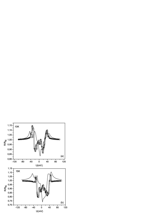
We have shown representative plots of experimental and modelled normalized resistances for a Co/YBCO 50 x 70 m2 sample at 10 and 15 K in Figure 4. It can be pointed out that our modelled normalized resistance can follow the original experimental data. The values of (30) and (27 meV) are also very close to those reported in the literature.tedro We kept here, since proximity effect is not important for a FM/high-TC junction like Co/YBCO. Actually, ferromagnetic material (like Co) breaks the cooper pairs.
If cooper pairs can not be formed in Co, proximity layer will not exist.
But, there is some difference between modelled and experimental normalized resistance in magnitudes along the vertical axis. This enhancement in normalized resistance and occurrence of extra peaks can be caused by the critical current which will be discussed in the next section.
IV.1 Effect of critical current
There are additional resistance peaks in AR data at a bias larger than the superconducting gap (eV ). This is not predicted by BTK theory.goutam Furthermore, an anomalous enhancement in the sub-gap conductance (eV ) in
nanoscale pinhole junctions is observed. This may sometimes become significantly larger than the conductance doubling expected from the point contact AR process.hind
When the region of the FM/high TC junction is driven into the normal state due to current-induced pair breaking as the current becomes larger than , additional peaks in differential resistance may be measured. If the contact current density depending on the effective contact area increases above the critical current density , the superconductor is transformed into a normal conductor.
It is possible to estimate the effective area of a N/SC junction from its normal state of conductance , where kF is the Fermi vector of the superconductor and is the effective contact area. For example, kF is 1 x 108 cm-1 for YBCO and in normal state the contact resistance amounts to 1M in case of = 50x70 Co/YBCO or Zn(Al,Co)O/YBCO junction, and amounts to 40 x 10-6 nm2.
Note that the effective contact area () is much smaller than the total area () in this kind of high resistance FM/high TC junctions. If for example a 40 pA current passes across the junction, the current density () will be around 1x10⁸ A/cm2, whereas the for YBCO lies around 3x10⁷ A/cm2 at 4.2 K.beck Hence, it is important to take into account the effect of critical current in the modelling. In order to do that, we have subdivided the total junction current into ICrit and IAR in the full energy range. The calculated I vs U curves are shown in Figure 5 (a). The slope in and outside the sub-gap region depends on the ICrit / IAR ratio.
Similarly, the junction resistance is divided into two series resistances. One is RAR which develops as the AR current passes across the junction. The other is RCrit which comes into play when the junction current crosses the limit . Simulation has been carried out considering the effect of the two subdivided junction resistances for the whole energy range and keeping the ratio of RCrit/RAR as a controlling parameter. It can be seen in Figure 5(b) how the increase of RCrit/RAR creates enhancement in resistance peaks in the sub-gap region. For RCrit/RAR=0 the plot agrees well with the prediction of BTK theory. It is clearly seen that with increasing RCrit/RAR ratio, the enhancement of resistance (or decrease of conductance) is more than the usual doubling described by the BTK model for ideal Andreev reflection.
V Conclusion
In conclusion, we have modelled the normalized resistance data of realistic FM/SC junctions. We have modified the original BTK formula with incorporation of proximity effect , spin polarization and broadening parameter for finite life time effects and interface scattering . We have demonstrated the occurrence of multi-peaks in normalized resistance data for Co/YBCO sample with 50x70 m2 contact area. In order to explain the multi-peak nature of AR, an additional voltage drop in terms of extra energy loss due to local electric fields at rough interfaces is included in the modified model. This accounts for the shift of the zero bias resistance dip in R/RN. Furthermore, we have explained the anomalous enhancement of normalized resistance due to the crossing of critical current limit across a FM/SC junction. The presented modified BTK formula may be used to model resistance peaks in the sub-gap region which have been experimentally observed at rough, large area FM/high TC junctions. Essentially, the model is useful because it can help to extract the value of spin polarization for FM and the superconducting gap parameter for SC from noisy differential resistance measurement data caused by junction interface inhomogeneities.
Acknowledgement
Partial financial support from Alexander von Humboldt foundation (N.G, INI 1120445 STP) and from BMBF (H.S, FKZ 03N8708) is gratefully acknowledged.
∗ Corresponding author:E-mail: ghosh.nilotpal@gmail.com, present address:Superconductivity Research and Application Section, Material Science Division, Indira Gandhi Centre for Atominc Research , Kalpakkam-603102, India
References
References
- (1) A.F. Andreev 1964 , 1823 [ 1964 , 1228].
- (2) G. E. Blonder, M. Tinkham and T. M. Klapwijk 1982 , 4515.
- (3) R. J. Soulen Jr., J. M. Byers, M. S. Osofsky, B. Nadgorny, T. Ambrose, S. F. Cheng, P. R. Broussard, C. T. Tanaka, J. Nowak, J. S. Moodera, A. Barry and J. M. D. Coey 1998 , 85.
- (4) S.K. Upadhyay, A. Palanisami, R.N. Louie and R.A. Buhrman 1998 , 3247.
- (5) G. J. Strijkers, Y. Ji, F. Y. Yang, C. L. Chien and J. M. Byers 2001 , 104510.
- (6) Y. Tanaka and S.Kashiwaya 1995 , 3451.
- (7) Y.S. Barash, A.V. Galaktionov and A.D. Zaikin 1995 , 665.
- (8) P. S. Luo, H. Wu, F. C. Zhang, C. Cai, X.Y. Qi, X. L. Dong, W. Liu, X. F. Duan, B. Xu, L. X. Cao, X. G. Qiu and B. R. Zhao 2005 , 094502.
- (9) Alexey V. Pan, S. Pysarenko, and S. X. Dou 2006 , 232506.
- (10) P.B. Mozhaev , F. Rönnung , P.V. Komissinskii , Z.G. Ivanov and G.A. Ovsyannikov 2000 , 93.
- (11) R. Rosenbaum, S-Y. Hsu, J-Y. Chen, Y-H. Lin and J-J. Lin 2001 , 10041.
- (12) M. Fogelstrom, D. rainer and J. Sauls 1997 , 281.
- (13) G. Sheet, S. Mukhopadhyay, and P. Raychaudhuri 2004 , 134507.
- (14) A. T. Hindmarch, C. H. Marrows and B. J. Hickey 2007 , 136211.
- (15) P. Szabo, P. Samuely, A. G. M. Jansen, P. Wyder, J. Marcus ,T. Klein and C. E. Filippini 1997 , 291.
- (16) R.C. Dynes, V. Narayanamurti and J.P. Garno 1978 ,1509.
- (17) H. Srikanth and A.K. Raychaudhuri 1992 , 229.
- (18) I.Iguchi and Z. Wen 1991 , 1.
- (19) M. Lorenz, H. Hochmuth, D. Natusch, M. Kusunoki and V. L. Svetchnikov 2001 3209.
- (20) M. Naito, H. Yamamoto and H. Sato 2000 , 201.
- (21) J. G. Ossandon, J. R. Thompson,D. K. Christen, Y. R. Sun, B. C. Sales, H. R. Kerchner,C J. E. Tkaczyk and K. W. Lay 1993 , 371.
- (22) N.Ghosh, J. Barzola Quiquia, Q. Xu, G. Biehne, H. Hochmuth, M. Lorenz, P. Esquinazi, M. Grundmann and H. Schmidt 2008 .
- (23) A. N. Mina , A. H. Phillips , F.M. Shaheen and N.S.AbdeI-Gawad 2000 ,301.
- (24) R. Beck, G. Leibovitch, A. Milner, A. Gerber, and G. Deutscher 2004 , 1069.
- (25) P. M. Tedrow and R. Meservey, Phys. Rev. Lett, , 192 (1971); Phys. Rev. B 7 (1973) 318.
Figure and Figure Captions