Low-temperature scanning tunneling microscopy of ring-like surface electronic structures around Co islands on InAs(110) surfaces
Abstract
We report on the experimental observation by scanning tunneling microscopy at low temperature of ring-like features that appear around Co metal clusters deposited on a clean (110) oriented surface of cleaved p-type InAs crystals. These features are visible in spectroscopic images within a certain range of negative tunneling bias voltages due to the presence of a negative differential conductance in the current-voltage dependence. A theoretical model is introduced, which takes into account non-equilibrium effects in the small tunneling junction area. In the framework of this model the appearance of the ring-like features is explained in terms of interference effects between electrons tunneling directly and indirectly (via a Co island) between the tip and the InAs surface.
pacs:
68.35.Dv, 68.37.Ef, 73.20.AtI Introduction
After the pioneering work of Tsui Tsui (1970), two-dimensional (2D) electron systems have been intensively investigated, in particular because of their huge application potential for the manufacturing of field effect transistors. Since then, a lot of success has been obtained with respect to improving the stability and the carrier mobility of the 2D electron gas. On the other hand, the 2D electron gas provides an excellent playing ground for studying the physical properties of low-dimensional systems. Up to now, the vast majority of experiments have been performed relying on tunneling contacts with planar geometry, where data is inevitably averaged and no local (on nanometer scale) information can be obtained. The nanometer size tunneling contact, which is created in scanning tunneling microscopy (STM) and scanning tunneling spectroscopy (STS) experiments, is able to directly provide such local information about the 2D electron gas.
Here, we present the results of local measurements of the electronic properties of a 2D system, which consists of metal Co islands deposited in situ on the (110) oriented surface of InAs that is obtained by cleavage in ultra-high vacuum (UHV) of a single crystal. It is well known that by deposition of only a small amount of different adsorbates onto the InAs(110) surface, the Fermi level can be shifted into the conduction band by up to (see, e.g., Betti et al. (2001); Morgenstern et al. (2002); Abe et al. (2002) and references cited therein), thus causing strong downward band bending and creating a 2D surface electron channel.
II Experiment and results
II.1 Experiment
We performed combined STM and STS measurements with a commercially available low-temperature STM www.omicron.de . The STM operates under UHV conditions at a base pressure in the range and at temperatures down to . In order to improve measurement stability, the whole UHV setup is decoupled from the building by a specially designed vibration isolation floor. Electrochemically preformed tungsten tips www.omicron.de , which are flash annealed in situ at elevated temperatures, are used. The tip quality is routinely checked by acquiring atomic-resolution images for the “herringbone” reconstruction of the Au(111) surface.
Spectroscopic measurements were performed in the current imaging tunneling spectroscopy (CITS) mode Wiesendanger (1994) with a grid size up to points. Additionally, we relied on harmonic detection with lock-in amplification for “hardware” measurements of the differential conductance. The excitation frequency was in the range , while the excitation amplitude was in the range .
The investigated InAs samples are doped with Mn at a doping level of . At this doping level Mn in InAs is expected to act as a shallow acceptor with ionization energy around . InAs slabs with size were cleaved in-situ at room temperature in the UHV preparation chamber (base pressure is about ) that is attached to the UHV STM chamber. Co islands were deposited by means of electron-beam evaporation at a rate of monolayer (ML) per second. The evaporation rate was calibrated by determining with x-ray reflectometry the thickness of thick Co films. As discussed in more detail below, the evaporation rate inferred from STM images of the Co islands on the InAs surface can deviate considerably from the calibrated rate.
For the InAs(110) surface, filled and empty surface bands are located deep inside the conduction and valence bands, respectively, and are separated by a surface gap Carstensen et al. (1990); Andersson et al. (1998) for a clean surface. Under clean conditions the bands are either flat, or a weak accumulation layer is formed on the surface Olsson et al. (1996). However, surface states can be strongly affected within 2 to 3 hours when the base pressure exceeds Karlsson et al. (1998). In order to prevent any undesirable effects of adsorbate induced surface degradation, we always keep the pressure below in the preparation chamber of our UHV setup during the different sample manipulations.
All the reported STM/STS experiments are performed at liquid helium temperature (). Everywhere in the text the tunneling bias voltage refers to the sample voltage, while the STM tip is virtually grounded. The experiments consist of three stages. First, the clean surface of a cleaved p-type Mn doped InAs(110) single crystal is characterized in detail by STM/STS measurements. Second, Co metal atoms are deposited on the InAs(110) substrate that is still cold (well below room temperature) after removal from the STM chamber. The amount of Co deposited on the surface is about . Deposition of a monolayer is according to the definition given in Morgenstern et al. (2002). Third, the Co-InAs system is investigated by STM/STS measurements.
II.2 2D surface of Co-InAs
Color online.
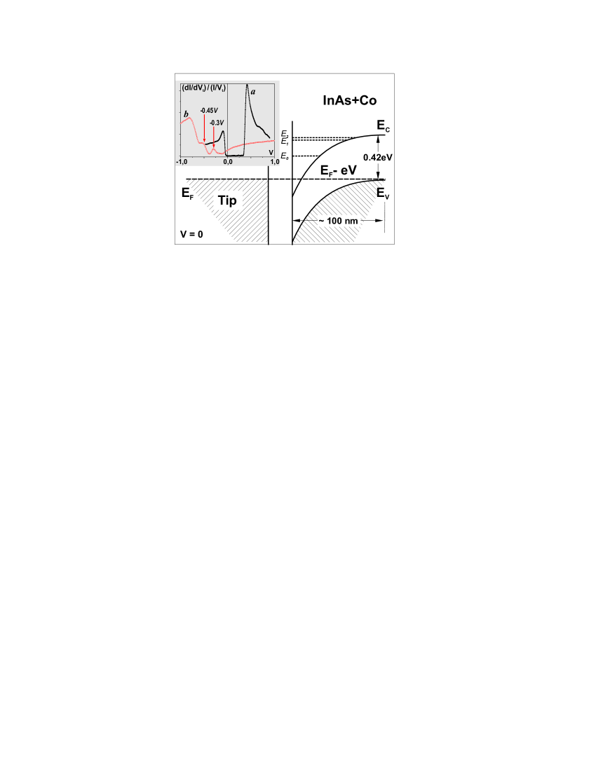
The quality of the clean cleaved InAs(110) surface is first carefully checked. Stable STM images of the surface reveal (1x1) relaxation with typical “butterfly” type of patterns appearing at the Mn doping atom sites Arseev et al. (2003), superimposed upon the InAs atomic lattice (see Fig. 2(a)). Mn atoms can be visualized in the first few subsurface layers. Our STS measurements clearly confirm the p-type character of the surface conductivity (see inset in Fig. 1, curve a), as expected for Mn doped InAs. After deposition of a very small amount of Co atoms (only ) onto the surface, the general outlook of the normalized () tunneling conductance curves drastically changes (see inset in Fig. 1, curve b). The Fermi level is now positioned about above the conduction band bottom. Two distinct peaks are visible on the normalized tunneling conductance curves around and around .
In order to provide a consistent explanation for the observed tunneling conductance curves, we need to take into account surface band bending (see Fig. 1). Co clusters are acting as “donors” when grown on a clean InAs(110) surface Morgenstern et al. (2002). The Co clusters are positively charged and downward band bending occurs at the surface. We note that the average value of the positive charge residing on a cluster is not an integer multiple of a single electron charge Maslova (2002).
Since our results indicate that , with the conduction band edge, and keeping in mind that the band gap for InAs is at Vurgaftmana et al. (2001), we then obtain a band bending at the surface that is as large as . This gives rise to a deep quantum well with a few discrete eigenstates. The binding energy of the lowest eigenstate (obtained by solving the Poisson-Schrödinger equation following Betti et al. (2001)) is . Consequently, the eigenstate is located almost above , or above . To make this state visible in the tunneling conductance curve, it has to be shifted inside the tunneling window , and this can be achieved by making the tunneling bias voltage sufficiently negative. When the eigenstate reaches , a peak will appear in the normalized tunneling conductance curve. We assume that this happens at a sample bias voltage of about for our experiments. The next peak appearing in the normalized tunneling conductance curve at can be assigned in a similar way to the fact that the eigenstate falls below . This is similar to what was described for the GaAs(110) surface in Feenstra et al. (2002).
The top of valence band, , is located below the Fermi level. Consequently, at bias voltage the width of the depletion layer is relatively small, and a tunneling current is able to flow from the InAs valence band to the tip. This can explain why the peak at is superimposed on a wide shoulder that results from the bulk valence band states (see inset in Fig. 1, curve b)
II.3 Rings around Co clusters
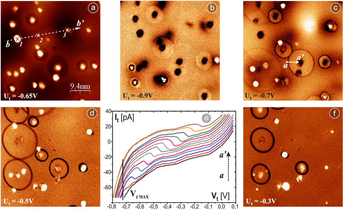
According to the results of our STM measurements, Co atoms tend to form small clusters on the InAs(110) surface despite the low substrate temperature during deposition. A typical STM image of a Co-InAs surface is presented in Fig. 2(a). From Fig. 2(a) we infer that the average cluster size is around for a tunneling bias voltage of . It is important to explicitly refer to the value of the tunneling bias voltage when analyzing topographical STM images, because the apparent size of the Co clusters strongly depends on the applied bias voltage. The majority of the clusters are one monolayer in height. A rough estimate gives an average number of Co atoms in a cluster (assuming a Co atom diameter of about ) that is around 30 atoms. There are 21 Co clusters on the STM image in Fig. 2(a), which has a size of . Consequently, the coverage that is inferred from Fig. 2(a) is , i.e., 3 to 4 times larger than the coverage obtained from the calibrated deposition rate.
A very intriguing observation in our STM images of the Co islands on the InAs(110) surface is the observation of ring-like features that appear around the Co clusters. In Fig. 2(a) one observes more or less circular depressions with sharp edges around some of the Co clusters. A surprising fact about these depressions is that the depressions have a different diameter at the same value of the bias voltage for clusters that look very similar in the STM image. In previous STM experiments Wildöer et al. (1996), similar features were observed around metal clusters of unknown origin.
In order to obtain a more detailed insight into the appearance of the ring-like features, we performed spatially resolved spectroscopic measurements above the same surface area where the STM image was obtained (Fig. 2(a)). In a first set of experiments, we relied on imaging based on harmonic detection with a lock-in amplifier. The results are shown in Figs. 2(b), (c), (d) and (f). Each image corresponds to a map of the tunneling current response at the frequency that is used for the modulation of the tunneling bias voltage. In a first approximation, this response is proportional to the value of the local density of states (LDOS) according to the relation
Next, we performed high-resolution CITS measurements with grid size of points. Figure 2(e) shows a set of curves acquired in the CITS mode along the cross-section indicated in Fig. 2(c). Regions with negative slope, which corresponds to a negative differential conductance (NDC), can be clearly observed on all but the two lowest curves. The latter two curves were acquired near point , i.e., at points that are at the largest distance from the cluster. The closer to the cluster the dependence is measured, the lower in absolute value is the tunneling voltage at which the region with NDC occurs. This experimental finding remains intact for STM tip to cluster distances down to a few tenths of . Comparing Fig. 2(e) with Figs. 2(b), (c), (d) and (f), we come to the conclusion that the distance between the STM tip and the cluster determines the bias voltage around which the NDC occurs on the curve. A dark ring with radius , which can be directly related to the presence of the NDC occurring around , will appear on the image taken near the bias voltage .
From our analysis of the results shown in Fig. 2 we conclude that (i) sharply defined dark rings appear in the differential conductance (LDOS) images around some of the clusters within a certain range of negative tunneling bias voltages, (ii) the size of the dark rings is shrinking when the absolute value of the tunneling bias voltage is decreased, and (iii) the LDOS has an almost constant value above the Co-InAs surface except for the clusters and the immediate vicinity of the dark rings. The only image, which reveals pronounced spatial variations of the normalized tunneling conductance, is image Fig. 2(c), taken at the threshold value of the tunneling bias voltage that approximately corresponds to the bias voltage where the ring radius reaches a maximum (see Fig. 2(e)). We assume that the presence and the different diameters of the dark rings around the different clusters is caused by the different bonding of the clusters to the InAs substrate. This assumption is supported by the fact that different Co clusters look quite differently on STM images taken at the same value of the tunneling bias voltage. curves also strongly differ when measured above different clusters. Curves, which are measured above clusters that are surrounded by a ring-like feature, reveal the presence of a narrow plateau (width of about ) around the Fermi level. On the other hand, clusters, which are not surrounded by a ring-like feature, reveal the presence of a wider plateau in the curve (width is ). These findings clearly require further investigation.
The maximum observable ring radius is determined by the fact that the region with negative differential conductance (see Fig. 2(e)) becomes masked by the rapidly growing tail of the characteristics at more negative bias voltages. For the Co clusters in the selected area this masking occurs for voltages while for other areas the value of will be different. In this bias voltage range the behavior of the tunneling conductance becomes much more complicated. As can be seen in Fig. 2(b), ring-like protrusions are observed in the LDOS image rather than ring-like depressions. Some of the rings become partly dark and partly bright. For these more negative bias voltages, the exact relation between the local slope of the curve and the depression of the tunneling current becomes important. More subtle details, such as the presence of neighboring clusters, impurity atoms or surface defects, will then have a pronounced influence on the imaging of the clusters.
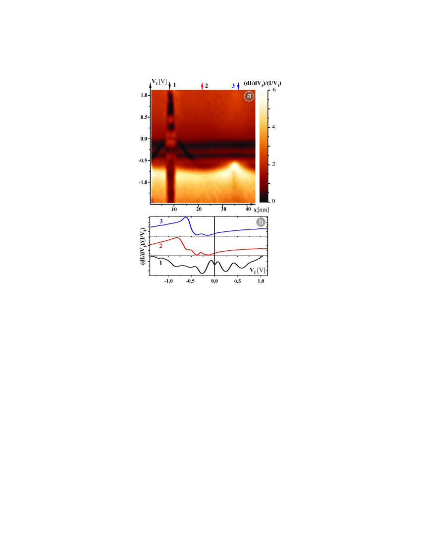
The large grid size that has been used for acquiring the CITS data allows us to present the data in another interesting way. Figure 3(a) gives a 2D map of the variation of the normalized tunneling conductance data along the cross-section in Fig. 2(a). The horizontal axis corresponds to the spatial coordinate, while the vertical axis corresponds to the tunneling bias voltage, and the color intensity corresponds to the measured value of the normalized tunneling conductance (LDOS). In Fig. 3(b) we show at the three points that are marked by the crosses on the cross-section in Fig. 2(a). These three points (1, 2, and 3) are marked in Fig. 3(a) as well.
From Fig. 3(a) it is clear that a Co cluster affects the LDOS in the conduction and valence bands only very locally. Except for a limited voltage range near , the influence of a cluster on the LDOS is very rapidly decaying outside the cluster. Inside the cluster, the conductivity in the valence band is considerably suppressed. Some of the energy levels of the Co cluster become visible in the voltage range corresponding to the band gap and the conduction band. In Fig. 3(a) there are two tilted dark lines that approximately start from the peak in the normalized tunneling conductance of the cluster and that extend over a distance of about into the defect free surface area. These two dark lines directly reflect the presence of the dark rings around the clusters as well as the dependence of the ring diameter on the tunneling bias voltage, which is clearly non-linear.
The two peaks in the normalized tunneling conductance at and at (see curve (a) in the inset to Fig. 1) also appear in Fig. 3(a) in the defect free surface area. The peaks are visible as perfectly straight, horizontal stripes. This implies that there occurs no noticeable change in the “rigid” (both bands move together) band shifts relative to the original bands of the p-type InAs. This is rather surprising, because a charged cluster and a charged impurity atom, separated by a distance of about , are surrounding the scanned area, and one might therefore expect changes to occur in the measured band shift. The absence of changes in the rigid band shift may be accounted for in the following way. First, both the Co cluster and the Mn impurity atom can be treated as point charges. It is known that a point charge potential does not strongly affect the band bending, but rather gives rise to fine structure in the LDOS Maslova (2002). Second, the variations of the LDOS around the Co cluster are strongly confined in space, while the Mn impurity atom alters the LDOS mostly near the top of the valence band. Hence, the conduction band remains almost undisturbed, with the conduction band bottom appearing as a straight line in Fig. 3(a). When the tunneling bias voltage , which is sweeping during the measurements of the tunneling conductance, reaches the band gap region and goes down to the top of the valence band, the energy levels of the 2D quantum well become populated. Taking into account the very high electron mobility along the surface Voronina et al. (2006), we may assume that in this bias range perfect screening by the 2D electron gas is taking place, hiding other details in the electronic structure.
On the other hand, when the 2D subband is shifted below the Fermi level, the tunneling bias dependent band bending noticeably slows down. This can be accounted for by the overlapping of the higher 2D subbands, which form a relatively wide continuum of states, thus pinning the Fermi level in this continuum. In this case the surface band structure “stabilizes”, i.e., an increase of the absolute value of the negative bias voltage leads only to slight changes in 2D subband energy.
Another important observation related to Fig. 3(a) is the influence of the Mn impurity atoms on (below) the Co-InAs(110) surface on the tunneling spectra. In the vicinity of a Mn atom the LDOS is affected deep inside the conduction and valence bands (not visible in Fig. 3(a)). Additionally, an intense peak appears in Fig. 3(a) near the valence band top and most probably this peak reflects the energy position of the Mn acceptor band. We note that the spatial extent of this peak is relatively large, about .
III Discussion
In order to explain the observed effects consistently one needs to take into account the presence of non-equilibrium and interference effects in the small tunneling junction Arseev et al. (1998), which can be described using the Keldysh diagram technique.
We need to explain two main peculiarities that are related to the observation of the ring-like features. First, the presence of the NDC region in the tunneling conductivity curves has to be accounted for. Second, the limited spatial extent of the circular features requires an explanation. Accordingly, this discussion section has been divided into two subsections.
III.1 Negative differential conductance
We start from the following model Hamiltonian :
where
describes the non-interacting electrons in the two electrodes: tip states , and bulk states . The part corresponds to the electron states in the cluster:
where the operator () destroys (creates) an electron in the cluster with spin . The part describes the electron states in the quantum well resulting from the Co cluster deposition and the STM tip induced band bending:
where () destroys (creates) an electron with spin in the quantum well, is the number labeling the 2D bands and is the 2D wavevector. is responsible for tunneling transitions from the quantum well and from the cluster into each of the electrodes (tip or substrate):
, , and are the relevant tunneling matrix elements: for tunneling from the cluster level to the quantum well subbands, for tunneling from the cluster level to the STM tip continuum, for tunneling from the quantum well level to the bulk of the semiconductor, for tunneling from the quantum well level to the STM tip.
The differential tunneling conductance can then be written as Hofstetter et al. (2001); Arseev et al. (2002)
| (1) |
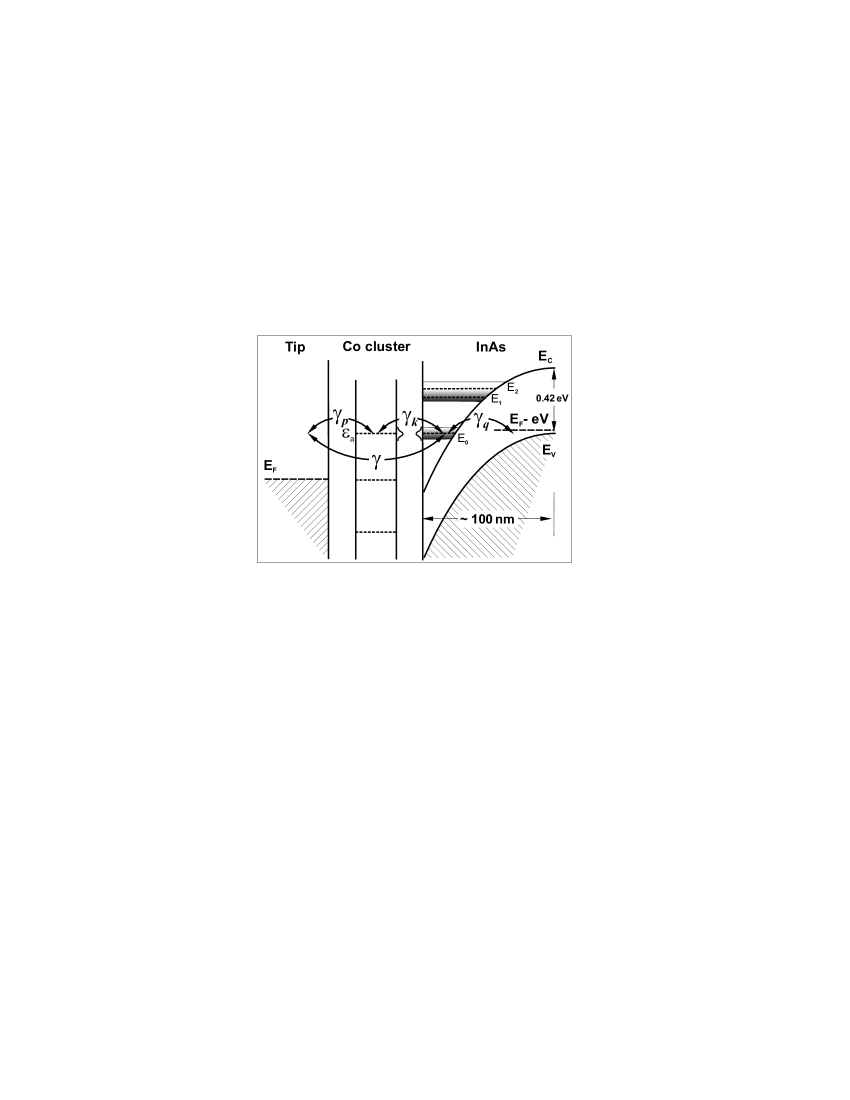
were , and are the density of states in the quantum well, the STM tip and the bulk semiconductor, respectively. The cluster density of states is proportional to .
The different tunneling rates in Eq. (III.1) are defined as follows (see Fig. 4): is the tunneling transition rate from a cluster level to the quantum well subbands, is the tunneling transition rate from a cluster level to the STM tip, is the tunneling transition rate from the quantum well to the bulk of the semiconductor, and is the tunneling transition rate from the quantum well to the STM tip. Finally, is defined as . We omit the subband index , because only the lowest subband plays the most important role in our model.
As stated above, a Co cluster acts as a donor, and consequently it is positively charged. In case of non-equilibrium, the energy of a cluster level , which is participating in the tunneling (see Fig. 4), depends on the electron filling number of this level:
where is the unperturbed position of the cluster energy level, is the equilibrium cluster level filling number, and is the Coulomb interaction energy of the localized charges Arseev et al. (1998).
For STM junctions we can assume that , because is of order of tunneling rates and , where is the width of conduction (valence) band in InAs. Equation (III.1) then reduces to
| (2) |
where refers the the extra contribution to the tunneling conductance resulting from the non-equilibrium effects.
Here is the pase angle, ascuired due to difference of wavefunctions of direct (STM tip-2D subband) and indirect resonant tunneling. The complicated coefficient in front of and the presence of in Eq. (III.1) also results from interference between direct tuneling from the STM tip to a quantum well subband, and indirect resonant tunneling via the cluster level. Consequently, the involved tunneling rates determine the sign and the magnitude of the additional current resulting from the non-equilibrium and interference processes.
For each tip position the value of is fixed, while can be varied by changing the applied bias voltage. depends on the relative position of the cluster level and of the first 2D subband . Both energies are bias dependent: trough and through the band bending. It is important to note that the 2D subband is relatively narrow. Electrons can be injected into this subband either from the STM tip () or from the Co cluster (). In both cases the wavevector component parallel to the surface, , is small. In close analogy with angle resolved photoemission spectroscopy experiments Aristov et al. (1999), only a narrow range of energies is available for tunneling into the 2D subband (see Fig. 4). In general, the component needs to be taken into account in STM experiments Jäger et al. (2003).
We assume that the unperturbed Co cluster energy level (at zero bias voltage) is positioned close to below the first 2D subband , i.e, the two energy levels are not aligned. This assumption is strongly supported by the experimental STS data (see Fig. 3 for details).
We now proceed with a more detailed analysis of the bias voltage dependence of . The first term in Eq. (III.1), which varies proportional to the cluster density of states, can change its sign. If (let us assume ) the sign of the coefficient that appears in front of is negative. For the assumed conditions, the coefficient that appears in front of is much smaller than the coefficient next to . The tunneling conductance curve is an inverted Lorentzian-shaped curve that is slightly asymmetric because of the contribution. The position of the dip in the tunneling conductance curve can be connected to the dependence. The closer to the cluster the STM tip is, the higher is the value of and the lower is the value of the non-equilibrium filling . The cluster energy level is pushed higher, and the dip in the tunneling conductance curve can be observed at smaller absolute values of the applied bias voltage (see Fig.2). The dark rings that appear in the STS images shrink when the absolute value of the negative tunneling bias decreases within a cluster dependent range of negative voltages.
III.2 Spatial extent of ring-like features
The most probable physical mechanism causing the formation of narrow (of the order of the interatomic distance) ring-like features in real space is some kind of resonant tunneling. When the STM tip changes its spatial position, localized energy levels that participate in the tunneling processes are coming out of resonance or even are falling outside the tunneling window . We find that the simple cluster charging model used in Wildöer et al. (1996); Koenraad is not adequate for describing our Co-InAs system. This is mainly due to the fact that on-site Coulomb repulsion for the cluster is the strongest bias dependent effect. This leads to variations of the cluster level filling number, and consequently to changes in the cluster level energy. Starting from this finding we are able to analyze in the framework of our model how spatially narrow circular features can be formed around the Co clusters.
For each value of the tunneling bias voltage the value of can be altered by changing the STM tip to cluster distance. Consequently, , which depends on the ratio also changes, giving rise to a shift of and to variations of . When moving the STM tip farther away from the cluster, is decreasing, leading to an increase of and to a lowering of . At a certain distance , the cluster energy level starts to becoming out of resonance with the narrow 2D subband . Since there is now an alignment with the tail of the broadened level, the value of the tunneling current drops. At the same time, the value of decreases, resulting in a decrease of the non-equilibrium occupation , and consequently is pushed higher. The cluster level then jumps to its equilibrium position . We assume that at the STM tip to cluster distance the tunneling rate , which exponentially decreases with increasing distance, becomes negligible (). The STM tunneling system does no longer feel the STM tip - cluster interaction, and the value of the tunneling current returns to its “normal” value. In other words, when at a certain tunneling bias voltage in the range where a dark ring appears in the LDOS around the Co cluster, the STM tip to cluster distance reaches the value , some kind of positive feedback, caused by mutually coupled variations of and , switches on. This positive feedback abruptly shifts the cluster energy level out of resonance with the 2D subband. This can account for the very small spatial width of the rings that appear in the LDOS as well as for the non-linear dependence of the ring diameter on the STM tip to cluster distance (see Fig. 3).
We note that for specific tunneling conditions the first term in Eq. (III.1) can become positive, causing the observation of bright rings or protrusions in the images of the differential conductance. A dark ring can turn into a bright one at high values of the tunneling bias voltage, as can be seen in Fig. 2(b).
Our theoretical model does not include any assumptions concerning the physical origin of the localized states through which resonant tunneling can occur. Therefore, this model should also be applicable to the case of an individual impurity atom near the surface. Ring-like features around individual impurities were indeed observed in our experiments (to be published) as well as on the GaAs(110) surface Koenraad .
IV Conclusion
In conclusion, relying on combined STM and STS measurements at low temperature, we have been able to identify the presence of ring-like features around Co metal clusters on a p-type InAs(110) surface that is prepared by in situ cleavage of a single crystal in UHV. The ring-like features become clearly visible in the maps of the differential normalized conductance for a certain range of negative tunneling bias voltages, due to the presence of a region with negative differential conductance in the dependence. The diameter of the rings is decreasing when decreasing the absolute value of the tunneling bias voltage. The possibility to observe the ring-like features around a Co cluster depends on the bonding of the cluster to the InAs(110) surface.
A theoretical model was developed, which takes into account the non-equilibrium effects that occur in the small STM tunneling junction. The model we propose allows us to explain the main experimental findings. In the framework of the model the appearance of the ring-like features structures is accounted for by the interference of direct (between the STM tip and the QW) and indirect tunneling via a Co cluster.
Acknowledgements.
This research in Moscow has been supported by the RFBR grants 05-02-19806-MF-a and 06-02-17076-a. The research in Leuven has been supported by the Fund for Scientific Research - Flanders (Belgium) as well as the Research Fund of the K.U.Leuven. We thanks A. A. Ezhov for the technical support. The authors also thank the WSxM team (www.nanotec.es).References
- Tsui (1970) D. C. Tsui, Phys. Rev. Lett. 24, 303 (1970).
- Betti et al. (2001) M. G. Betti, V. Corradini, G. Bertoni, P. Casarini, C. Mariani, and A. Abramo, Phys. Rev. B 63, 155315 (2001).
- Morgenstern et al. (2002) M. Morgenstern, J. Wiebe, A. Wachowiak, M. Getzlaff, J. Klijn, L. Plucinski, R. L. Johnson, and R. Wiesendanger, Phys. Rev. B 65, 155325 (2002).
- Abe et al. (2002) S. Abe, T. Inaoka, and M. Hasegawa, Phys. Rev. B 66, 205309 (2002).
- (5) www.omicron.de.
- Wiesendanger (1994) R. Wiesendanger, Scanning Probe Microscopy and Spectroscopy (Cambridge University Press, 1994).
- Carstensen et al. (1990) H. Carstensen, R. Claessen, R. Manzke, and M. Skibowski, Phys. Rev. B 41, 9880 (1990).
- Andersson et al. (1998) C. B. M. Andersson, J. N. Andersen, P. E. S. Persson, and U. O. Karlsson, Surf. Sci. 398, 395 (1998).
- Olsson et al. (1996) L. Ö. Olsson, C. B. M. Andersson, M. C. Håkansson, J. Kanski, L. Ilver, and U. O. Karlsson, Phys. Rev. Lett. 76, 3626 (1996).
- Karlsson et al. (1998) H. S. Karlsson, R. Viselga, and U. O. Karlsson, Surf. Sci. 402, 590 (1998).
- Arseev et al. (2003) P. I. Arseev, N. S. Maslova, V. I. Panov, S. V. Savinov, and C. Van Haesendock, JETP Lett. 77, 172 (2003).
- Maslova (2002) N. Maslova, Habilitation Thesis (Moscow State University, 2002).
- Vurgaftmana et al. (2001) I. Vurgaftmana, J. R. Meyer, and L. R. Ram-Mohan, Appl. Phys. Rev. 89, 5815 (2001).
- Feenstra et al. (2002) R. M. Feenstra, G. Meyer, F. Moresco, and K. H. Rieder, Phys. Rev. B 66, 165204 (2002).
- Wildöer et al. (1996) J. W. G. Wildöer, A. J. A. van Roij, C. J. P. M. Harmans, and H. van Kempen, Phys. Rev. B 53, 10695 (1996).
- Voronina et al. (2006) T. I. Voronina, T. S. Lagunova, M. P. Mikhailova, K. D. Moiseev, A. F. Lipaev, and Y. P. Yakovlev, Semiconductors 40, 497 (2006).
- Arseev et al. (1998) P. I. Arseev, N. S. Maslova, and S. V. Savinov, JETP Lett. 68, 320 (1998).
- Hofstetter et al. (2001) W. Hofstetter, J. König, and H. Schoeller, Phys. Rev. Lett. 87, 156803 (2001).
- Arseev et al. (2002) P. I. Arseev, N. S. Maslova, V. I. Panov, and S. V. Savinov, JETP 94, 191 (2002).
- Aristov et al. (1999) V. Y. Aristov, G. Le Lay, V. M. Zhilin, G. Indlekofer, C. Grupp, A. Taleb-Ibrahimi, and P. Soukiassian, Phys. Rev. B 60, 7752 (1999).
- Jäger et al. (2003) N. D. Jäger, E. R. Weber, K. Urban, and P. Ebert, Phys. Rev. B 67, 165327 (2003).
- (22) P. Koenraad, private communication.