Electric field effect on electron spin splitting in SiGe/Si quantum wells
Abstract
Effect of electric field on spin splitting in SiGe quantum wells (QWs) has been studied theoretically. Microscopical calculations of valley and spin splittings are performed in the efficient tight-binding model. In accordance with the symmetry considerations, the electric field not only modifies the interface induced spin splitting but gives rise to a Rashba-like contribution to the effective two-dimensional electron Hamiltonian. Both the valley and spin splittings oscillate as a function of the QW width due to inter-valley reflection of the electron wave off the interfaces. The oscillations of splitting are suppressed in rather low electric fields. The tight-binding calculations have been analyzed by using the generalized envelope function approximation extended to asymmetrical QWs.
pacs:
73.21.Fg, 78.67.DeI Introduction
Understanding the details of semiconductor heterostructure electronic properties has been a key at each stage of their applications in the field of information and communication technologies. Presently, there is a broad interest in spin-dependent properties because they have a potential for novel “spintronic” devices, and beyond, because they govern for a large part the possible development of semiconductor-based quantum information processing. Spin splitting of electron dispersion relations arises from the combination of spin-orbit coupling and inversion asymmetry. Besides the contributions of bulk inversion asymmetry (BIA) first discussed by Dresselhaus in 1954 and the structure inversion asymmetry (SIA) introduced by Rashba,Rashba (1960); Bychkov and Rashba (1984) the existence of a contribution due to the breakdown of roto-inversion symmetry at an interface between two semiconductors was first suggested by Vervoort et al. in the late 90s.Vervoort et al. (1997, 1999) This “interface inversion asymmetry” (IIA) term was further documented both by group-theoretical analysis,Ivchenko et al. (1996) envelope-function calculationsVervoort et al. (1999) and measurements of circular polarization relaxation in quantum wells (QWs) based on various III-V semiconductors.Guettler et al. (1998); Olesberg et al. (2001); Hall et al. (2003) However, in these cases, the interface contribution appears in combination with BIA and SIA. Pure IIA can exist alone or together with SIA in heterostructures of centro-symmetric semiconductors like Si-Ge QWs. Previous worksGolub and Ivchenko (2004) have established the symmetry properties specific to this system where electrons lie in states originating from the bulk Xz valleys. A general feature of zone-edge conduction valleys in bulk materials is their degeneracy (6 for X-valleys, 4 for L-valleys) that gives rise to strong valley-coupling when they are folded onto the two-dimensional Brillouin zone of a QW.Boykin et al. (2004); Nestoklon et al. (2006); Jancu et al. (2005); Valavanis et al. (2007); Virgilio and Grosso (2007); Friesen et al. (2007) Valley coupling is another manifestation of the local, three-dimensional variations of crystal potential at semiconductor interfaces and quantitative estimates require atomistic information which is not available within the theoretical framework. Parameters describing valley coupling must be extracted from microscopic approaches such as ab-initio calculations or modelizations using empirical parametrizations like atomistic pseudopotentials or tight-binding approach. The valley coupling strongly depends on the crystalline growth direction and shows an oscillating behaviour as a function of the number of monolayers forming the Xz-valley or L-valley quantum well. It also depends on the overall symmetry of the quantum well and for this reason, it can be modified by an external electric field. The spin-splittings of in-plane dispersion relations in such systems results from the interplay of valley coupling and spin-dependent terms in the electron Hamiltonian. The case of L-valley QWs formed in the GaSb-AlSb system and grown along the [001] direction was first discussed in some details by Jancu et al.Jancu et al. (2005) In that case, the leading terms come from BIA invariants specific to the L valleys in combination with the L-valley coupling. For Si-Ge (001)-grown QWs the interplay of IIA with Xz valley coupling was examined from the theory point of view and semi-quantitative estimates were discussed in the frame of tight-binding calculations based on the model.Nestoklon et al. (2006) However, it is well known that this simple model cannot reproduce quantitatively the properties of zone edge valleys such as effective masses and dipole matrix element. This difficulty was solved in the late nineties by the introduction of the extended basis tight binding model.Jancu et al. (1998) More recently, progress in the parametrization of this model have led to essentially perfect description of the electronic properties of bulk GeJancu and Voisin (2007) and Si.Sacconi et al. (2004) In this work, we use the advanced tight-binding model in combination with the envelope function approach and calculate the conduction band spin splitting resulting from the interplay of valley coupling with the IIA and electric-field effects in Si/SiGe quantum wells.
II Point-group symmetry analysis
In the virtual-crystal approximation for SiGe alloys, an ideal (001)-grown SiGe/Si/SiGe QW structure with an odd number of Si atomic planes has the point-group symmetry D2d which allows the spin-dependent term in the electron effective Hamiltonian, where are the Pauli spin matrices, is the two-dimensional wave vector with the in-plane components , and . The QW structures with even have the D2h point symmetry containing the space-inversion center, the constant is zero and the two-dimensional electronic states are doubly degenerate. Under an electric field applied along the growth direction the symmetry of QW structures with both odd and even numbers of Si monoatomic layers reduces to the C2v point group and the spin-dependent linear- Hamiltonian becomes
| (1) |
where the second contribution is usually called the Rashba term (or the SIA term). In order to establish the parity of with respect to inversion of the electric field we note that, in the D2d group, the combination as well as even powers of are invariants while both the combination and odd powers of transform according to the same representation B2 (in notations of Ref. Bir and Pikus, 1974). Therefore, for structures with odd , the coefficients and are, respectively, even and odd functions of . They can be presented as
| (2) | |||||
where and are field-independent coefficients. Similarly, for structures with even , the linear-in- spin-dependent Hamiltonian can be presented in the form
| (3) |
where are even functions of . The above representation follows immediately if we take into account that, with respect to operations of the D2h group, both and transform in the same way as the component does.
The aim of this work is to calculate and analyze the electric field dependencies of and . For this purpose we use the precise nearest-neighbor tight-binding model Jancu et al. (1998) and calculate valley and spin splittings in symmetrical QWs in the absence and presence of an external electric field.
III Tight-binding model
To calculate electron subband splittings, we use the tight-binding theory elaborated by Jancu et al.Jancu et al. (1998) It perfectly reproduces band structure of indirect bulk semiconductors as well as electron effective masses, etc. In particular the parametrization used in this work reproduces the value =85% of the conduction band minimum in Si, which was considered as a challenge.Klimeck et al. (2000) One of the main advantages of this method is a very straightforward treatment of nanostructures.
In Ref. Nestoklon et al., 2006, we estimated the electron spin splitting in symmetrical SiGe QWs using a less detailed tight-binding model, namely, the model, which allowed us to understand the main qualitative features of spin splitting as well as to demonstrate the possible observability of this effect in Si/SiGe heterostructures.
In the tight-binding model the electron wave function is written as a linear combination of atomic orbitals Slater and Koster (1954)
| (4) |
where enumerates atoms in the structure, runs through the set of spinor orbitals at the th atom. In the model, this set includes the orbitals , , and multiplied by the spinors and . We assume the basic orbital functions to be orthogonal. Anyway, this can be achieved using the Löwdin orthogonalization procedure. Löwdin (1950) Thus, the tight-binding Hamiltonian is presented as a multicomponent matrix and the Schrödinger equation as an eigenvalue problem
| (5) |
where . The Hamiltonian matrix elements depend on the relative position of atoms, , and chemical type of atoms and . We use here the nearest neighbour approximation where the matrix elements differ from zero only for neighbouring atoms. The detailed procedure of constructing the tight-binding Hamiltonian can be found in Ref. Slater and Koster, 1954. Strain effects can be included by scaling the matrix elements with respect to the bond-angle distortions and bond-length changes. Ren et al. (1982)
For the SiGe alloy we use the virtual crystal approximation (VCA) in order to concentrate on the intrinsic structure symmetry thus neglecting all effects of disorder. Tight-binding parameters were optimized to carefully reproduce alloy band structure. We treat strain in two independent ways: first, atomic positions used in calculations are chosen by using Van de Walle’s model.Van de Walle (1989) We have also applied Keating’s Valence Force Field (VFF) model Keating (1966) with the SiGe parameters from Ref. Bernard and Zunger, 1991 and found no difference between the continuous and atomistic approaches.
In addition to the strain dependence of tight-binding parameters we have corrected the structure potential (see below) with respect to experimentally observed Si/Si1-xGex conduction-band offset.Rieger and Vogl (1993); Schäffler (1997)
We treat an electric field in the tight-binding approach in the following way:Boykin and Vogl (2001) the diagonal matrix elements of the tight-binding Hamiltonian are shifted due to the potential of the applied electric field
| (6) |
where is the electric potential energy.
Since we are interested in the in-plane dispersion of free electrons in a heterostructure we impose periodical boundary conditions in the interface plane (001). Because of the periodicity in the [100] and [010] directions we can introduce the in-plane wave vector and, for a given value of , construct the tight-binding Hamiltonian with a discrete spectrum. For the sake of numerical simplicity we also use periodic boundary conditions along the growth direction [001] taking the barrier layers thick enough to exclude the influence of their thickness on the calculated values of and . It follows immediately from the band structure of silicon and SiGe/Si/SiGe structure potential that, neglecting the valley splitting, the electronic states with are four-fold degenerate. We will focus on the dispersion of the lowest conduction subband . The interface-induced valley mixing leads to a splitting of the state into two spin-degenerate states denoted (upper subband) and (lower subband). At nonzero each subband, and , undergoes the spin-orbit splitting described by Eq. (1) with the coefficients and for the valley-orbit split subbands . It is instructive to rewrite Eq. (1) in the coordinate frame as follows
| (7) |
Let us introduce the energy difference for the states with the spin polarized parallel and antiparallel to [110], and for the states with the spin polarized parallel and antiparallel to . The modulus of gives the spin splitting of the subbands and the sign of determines the relative position of the split spin sublevels. It follows from Eq. (7) and the definition of that the constants can be found from
| (8) | |||
Also it should be pointed out that, since the studied QWs are quite shallow, the electron dispersion should be treated with care. To avoid non-linear effects, very small values of should be considered.
IV Results and discussion
IV.1 Numerical model calculations: unbiased structure
In order to test and improve our previous results we calculated valley and spin splitting in symmetrical Si QW with Si0.75Ge0.25 barriers as a function of the QW width. For SiGe composition we used optimized tight-binding parameters precisely reproducing realistic alloy band structure. The strategy for parameterization of the Ge-Si alloy in a virtual crystal approximation is as follow: the parameters of Ge and Si hydrostatically strained to the alloy parameter are first calculated and linearly interpolated. The small remaining differences with measured values are then corrected by fine tuning of a few two-center parameters. For interface atoms we use linear combination of pure Si parameters and alloy.
Tight-binding parameters are optimised for bulk materials. However, band offsets at the interfaces in the heterostructure are also important. For conduction band offset we use Shäffler’s paper Schäffler (1997) as a reference. Thus, we take a value of 150 meV as a conduction band offset for Xz valley electrons.
Figure 1 shows the zero-field results of calculation of (a) the valley splitting and (b) the constants for the valley split subbands in a symmetrical single QW structure with Si atomic planes sandwiched between the thick Si0.75Ge0.25 barriers. The splittings as a function of exhibits oscillations, in agreement with Refs. Nestoklon et al., 2006; Boykin et al., 2004; Valavanis et al., 2007; Friesen et al., 2007. In Fig. 1 X-shaped crosses depicted as vortices of the broken line represent the calculation in the envelope-function approximation, see below. The broken line is drawn for the eye. Note that, in order to simplify comparison with results obtained by other authors, Fig. 1a illustrates the valley splitting not only for the QW width region 1550 Å but also for the region 6070 Å.

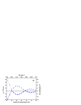
Results obtained in the framework of the advanced tight-binding model show considerable difference with our previous estimations.Nestoklon et al. (2006) The valley splitting is significantly smaller, its value decreases by a factor of 3, whereas the spin splitting increases almost six times. This difference is not unexpected since a careful tight-binding treatment of Si and its compounds is possible in the model only. In this regard the goal of the previous paper Nestoklon et al. (2006) was to demonstrate that the effect of spin splitting in macroscopically symmetrical Si quantum wells is measurable and to reveal the main qualitative properties of this splitting.
The previous theoretical values for valley splitting were obtained by both tight-bindingBoykin et al. (2004); Friesen et al. (2007) and pseudopotential methods.Valavanis et al. (2007) Although the first two papers utilize the method of calculation similar to that applied here, a straightforward comparison is not possible due to different parametrizations of the Si1-xGex alloy, different alloy compositions ( = 0.2 in Ref. Boykin et al., 2004 and 0.3 in Ref. Friesen et al., 2007) and conduction band offsets used. However, our results are in good agreement with the both estimations. For example, for a QW containing 64 Si-atomic layers (32 monomolecular layers, 9 nm) we obtain for the valley splitting meV , while Refs. Boykin et al., 2004 and Friesen et al., 2007 present the coinciding values of . Our analysis shows that the valley splitting is quite sensitive to the SiGe alloy parameters. By using the linear combination of Si and Ge tight-binding parameters for the alloy we could reproduce values of the valley splitting obtained by Boykin et al.Boykin et al. (2004)
Comparison with Ref. Valavanis et al., 2007 is more straightforward. Figure 1 in the cited paper shows dependence of the valley splitting on the barrier Ge content for a 16 Si-atomic layer QW calculated by the empirical pseudopotential method. In particular, for the Si0.75Ge0.25/Si/Si0.75Ge0.25 QW the valley splitting of about 2.5 meV was obtainedValavanis et al. (2007) while our estimation is 3.7 meV. This is a good agreement taking into account that the two values are obtained in two completely different approaches for quite narrow QWs where interface effects are extremely important.
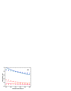
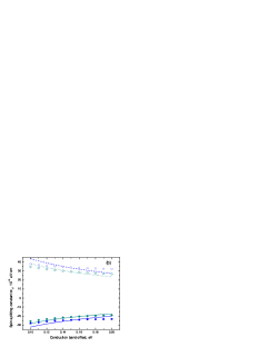
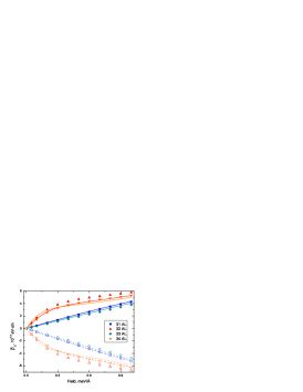
Figure 2 shows the valley and spin splitting constants as a function of the conduction band offset for QWs with 31, 32, 33, 34 and 64 Si atomic layers. The fifth structure is taken in order to provide comparison with Refs. Boykin et al., 2004; Friesen et al., 2007. In Fig. 2, in addition to the tight-binding calculations, we present analytical results on valley and spin splitting in the framework of the extended envelope function approach. A detailed discussion of the analytical treatment is given in subsection IV.3. Here we only point out an excellent agreement between results for the splittings as a function of the QW width and satisfactory description of the dependence of these splittings on the band offset.
IV.2 Numerical calculations in the presence of electric field
Figure 3 demonstrates the variation of spin splitting constants with the electric field for the valley-split subbands. In accordance with symmetry considerations, the calculations show that the spin splitting becomes anisotropic in QWs with odd numbers of atomic planes and appears in QWs with even numbers of atomic planes. The variation of valley splitting is very weak and we do not present it here.
In order to determine the coefficients and we performed the tight-binding calculation of the spin splittings for the electron wave vectors and and then applied Eq. (8) to find the constants and directly. The electric field is introduced as a shift of diagonal energies in the tight-binding Hamiltonian. In accordance with Eq. (6), we choose electrostatic potential to be a linear function of both inside the QW and in the barrier areas near the interfaces. The area of the constant electric field is extended inside barriers enough to neglect dependence of the splitting on the choice of potential profile. Note that the field values in Fig. 3 are small enough to avoid the tunnelling of an electron from the QW inside the barrier.
At zero electric field, =0 for arbitrary value of and, similarly, for even . In this case the spin splitting is independent of the azimuthal angle of the vector. However, with increasing the field the diversity in values of and for QWs with decreases.
The further discussion of spin splitting as a function of electric field is continued in the next section. It suffices to note here that within the chosen range of field values, the coefficients in QWs with odd are linear functions of . In contrast, in QWs with even numbers of atomic planes where the spin splitting is absent at zero field, are proportional to . We stress that the field-induced change of (odd ) becomes comparable to the zero-field value of in quite weak fields V/cm.
In the previous paperNestoklon et al. (2006) we developed the extended envelope function model in order to demonstrate that the spin splitting in macroscopically symmetrical QWs is fully defined by interfaces. At non-zero electric field two mechanisms are possible, namely, the SIA and IIA mechanisms. One of the goals of current research is to establish the most important term in realistic QWs. To reveal carefully the comparative role of two mechanisms we present analytical treatment of results shown in Figs. 2 and 3 in the framework of the envelope function approach.
IV.3 Extended envelope function approach
Here we propose an extended envelope function approach Nestoklon et al. (2006) to describe valley and spin splittings in the presence of an external or built-in electric field. The electron wave function is written as
| (9) |
where is the Bloch function at the the extremum points on the line in the Brillouin zone. The spinor envelopes in Eq. (9) are conveniently presented as a four-component bispinor
| (10) |
The effective Hamiltonian acting on is written as a 44 matrix consisting of the standard zero-approximation Hamiltonian
| (11) |
which is independent of valley and spin indices, and an interface-induced -functional perturbation
| (12) |
Here and are the longitudinal and transverse electron effective mass in the valley of the bulk material, and are the coordinates of the left- and right-hand-side interfaces, the potential energy is referred to the bottom of the conduction band in Si and given by
with being the conduction-band offset, in the SiGe barrier layers and inside the Si layer. The explicit form of the matrices obtained by using symmetry considerations is presented in Ref. Nestoklon et al., 2006.
In the zero approximation, i.e., neglecting the valley-orbit and spin-orbit coupling, , the bispinor is given by
where are arbitrary -independent spinors and the function satisfies the Schrödinger equation
| (13) |
In the following we take into consideration only the lowest size-quantized electronic subband .
The next step is an allowance for the interface-induced spin-independent mixing between the valleys and described by the matrices
where , , is the QW width, is the microscopic lattice constant, and is a complex coefficient.
In terms of the envelope the matrix element of valley mixing can be written as
| (14) |
where and are the modulus and the phase of , are the values of the envelope at the right and left interfaces, , respectively. The valley-orbit split states have the energy , where is the eigen energy of Eq. (13), so that the splitting is equal to
| (15) |
The bispinors for the upper () and lower () states are given by
| (16) |
where is spinor for the electron spin and for the electron spin , is the phase of the matrix element (14).
The tight-binding calculations show that the spin splitting is much smaller as compared to the valley splitting . Therefore, the spin splitting can be considered independently for the upper and lower valley-orbit split states (16). The corresponding matrix elements are reduced to
| (17) |
where the subscript indices enumerate the valleys , and are the spin indices, the components written as 22 matrices are related to similar 22 matrices , , , by
The spin-dependent contributions to , , , are linear combinations of and , see Ref. Nestoklon et al., 2006:
| (18) |
and similar equation for with the coefficients interrelated with due to the mirror-rotation operation (odd ) or the inversion (even ) which transforms the right-hand-side interface into the left-hand-side one. Taking into account the relation between coefficients entering the matrices and and the notations of Ref. Nestoklon et al., 2006 we can write the spin Hamiltonians (17) in the form of Eq. (1), namely,
| (19) |
For the coefficients describing the spin splitting of the valley-orbit split subbands, we obtain
| (20) |
Here
the parameters describe the intra-valley contributions to the interface-induced electron spin mixing, and the parameters , describe the spin-dependent inter-valley mixing. Oscillatory dependence of the valley and spin splittings on the QW thickness is caused by interference of electron waves arising from inter-valley reflection off the left- and right-hand side interfaces.
IV.4 Comparison between tight-binding and envelope function approach
In the absence of an electric field, one has , for positive and for negative values of , and Eqs. (15), (20) reduce toNestoklon et al. (2006)
for even , and
for odd , where . The curves in Fig. 1 are calculated by using the following best-fit set of parameters: meVÅ, 0.013, = meVÅ2, , = 650 meVÅ2.
Although tight-binding-model values of the coefficients in the present work are quite different from the previous estimations, the envelope function approach proves its adequate description of the valley and spin splittings as a function of the QW width. The analytical approach with merely five parameters perfectly fits the complex microscopical calculation.
Comparison of new results with experimental data of Wilamovsky et al.Wilamowski et al. (2002) shows the better agreement. With the necessary correctionGlazov (2004) the experimental results give eVÅ for the spin splitting constant in a 120Å-thick QW. The more detailed comparison should be done with caution since effects of disorder and built-in electric fields can have crucial influence. However, the coincidence in an order of magnitude shows that our calculations agree with the available experimental data.
According to Fig. 2, the description of dependence of spin splitting on the band offset is not so perfect in the framework of envelope function approach. In fact, the variation in band offset results in a complex (obviously non-linear) behaviour of the parameters in the boundary conditions at the interfaces.
Figure 3 is the main result of this work and we discuss it in more details. The agreement between the two approaches seen in Fig. 3a shows that the extended envelope function approach catches the physics of spin splitting induced by the applied electric field. Moreover, the fact that this agreement takes place with no addition of a SIA term shows that in the system under study the IIA contribution is dominating. It should be noted that Eq. (20) for contains only parameters which can be extracted from Fig. 1, and, indeed, Fig. 3a does not contain any fitting parameters. Additional fitting parameters used to describe Fig. 3b are as follows: = meVÅ2, and = meVÅ2.
In the high-field limit so that either or , and Eqs. (15), (20) transfer to
Since one of the interfaces becomes inaccessible to the electron the oscillatory behavior vanishes in strong fields.
It should be stressed that the parity of the coefficients and following from the above equations completely agrees with the general symmetry considerations, see Eqs. (2) and (3). We also note that a monoatomic shift as a whole of the QW position in the structure results in an inversion of sign of while the values of remain unchanged.
V Conclusion
The tight-binding model has been used to calculate the electron dispersion in heterostructures grown from multivalley semiconductors with the diamond lattice, particularly, in the Si/SiGe structures. The model allows one to estimate quantitatively the valley and spin splittings of electron states in the quantum-confined ground subband as well as the electric-field dependence of the spin splitting. In the employed tight-binding model, this splitting is mostly determined by the spin-dependent mixing at the interfaces. As a result the coefficients describing the Dresselhaus term in unbiased QWs are oscillating functions of the odd number of Si monoatomic layers. Under an electric field applied along the growth axis a non-zero Rashba term appears in QWs with both even and odd Si atomic layers. In small fields, the Dresselhaus term is linear in the structures with even ( point group) and quadratic in structures with odd ( point group). Thus, in quite low fields about eVcm the spin splitting becomes anisotropic and oscillations as a function of the QW width are suppressed. In addition to numerical calculations, an extended envelope function approach is utilized to interpret the results of tight-binding calculations. The inclusion of spin-dependent reflection of an electronic wave at the interface and interface-induced inter-valley mixing permits one to describe quite well the numerical dependencies of the valley-orbit and spin-orbit splittings upon the number of Si atomic planes and the electric field.
Acknowledgements.
This work was financially supported by RFBR and CNRS PICS projects, programmes of RAS and “Dynasty” Foundation — ICFPM.References
- Rashba (1960) E. I. Rashba, Fiz. Tverd. Tela 2, 1224 (1960), [Sov. Phys. Solid State 2, 1109 (1960)].
- Bychkov and Rashba (1984) Y. A. Bychkov and E. I. Rashba, Pis’ma Zh. Eksp. Teor. Fiz. 9, 66 (1984), [JETP Lett. 39,78 (1984)].
- Vervoort et al. (1997) L. Vervoort, R. Ferreira, and P. Voisin, Phys. Rev. B 56, R12744 (1997).
- Vervoort et al. (1999) L. Vervoort, R. Ferreira, and P. Voisin, Semicond. Science and Technology 14, 227 (1999).
- Ivchenko et al. (1996) E. L. Ivchenko, A. Y. Kaminski, and U. Rössler, Phys. Rev. B 54, 5852 (1996).
- Guettler et al. (1998) T. Guettler, A. L. C. Triques, L. Vervoort, R. Ferreira, P. Roussignol, P. Voisin, D. Rondi, and J. C. Harmand, Phys. Rev. B 58, 10179 (1998).
- Olesberg et al. (2001) J. T. Olesberg, W. H. Lau, M. E. Flatté, C. Yu, E. Altunkaya, E. M. Shaw, T. C. Hasenberg, and T. F. Boggess, Phys. Rev. B 64, 201301 (2001).
- Hall et al. (2003) K. C. Hall, K. Gündoğdu, E. Altunkaya, W. H. Lau, M. E. Flatté, T. F. Boggess, J. J. Zinck, W. B. Barvosa-Carter, and S. L. Skeith, Phys. Rev. B 68, 115311 (2003).
- Golub and Ivchenko (2004) L. E. Golub and E. L. Ivchenko, Phys. Rev. B 69, 115333 (2004).
- Boykin et al. (2004) T. B. Boykin, G. Klimeck, M. Friesen, S. N. Coppersmith, P. von Allmen, F. Oyafuso, and S. Lee, Phys. Rev. B 70, 165325 (2004).
- Nestoklon et al. (2006) M. O. Nestoklon, L. E. Golub, and E. L. Ivchenko, Phys. Rev. B 73, 235334 (2006).
- Jancu et al. (2005) J.-M. Jancu, R. Scholz, E. A. de Andrada e Silva, and G. C. L. Rocca, Phys. Rev. B 72, 193201 (2005).
- Valavanis et al. (2007) A. Valavanis, Z. Ikonic, and R. W. Kelsall, Phys. Rev. B 75, 205332 (2007).
- Virgilio and Grosso (2007) M. Virgilio and G. Grosso, Phys. Rev. B 75, 235428 (2007).
- Friesen et al. (2007) M. Friesen, S. Chutia, C. Tahan, and S. N. Coppersmith, Phys. Rev. B 75, 115318 (2007).
- Jancu et al. (1998) J.-M. Jancu, R. Scholz, F. Beltram, and F. Bassani, Phys. Rev. B 57, 6493 (1998).
- Jancu and Voisin (2007) J.-M. Jancu and P. Voisin, Phys. Rev. B 76, 115202 (2007).
- Sacconi et al. (2004) F. Sacconi, A. Di Carlo, P. Luigli, M. Städele, and J.-M. Jancu, IEEE Transactions on Electron Devices 51, 704 (2004).
- Bir and Pikus (1974) G. Bir and G. Pikus, Symmetry and Strain Induced Effects in Semiconductors (Wiley, New York, 1974).
- Klimeck et al. (2000) G. Klimeck, R. C. Bowen, T. B. Boykin, C. Salazar-Lazaro, T. A. Cwik, and A. Stoica, Superlattices and Microstructures 27, 77 (2000).
- Slater and Koster (1954) J. C. Slater and G. F. Koster, Phys. Rev. 94, 1498 (1954).
- Löwdin (1950) P.-O. Löwdin, The Journal of Chemical Physics 18, 365 (1950).
- Ren et al. (1982) S. Y. Ren, J. D. Dow, and D. J. Wolford, Phys. Rev. B 25, 7661 (1982).
- Van de Walle (1989) C. G. Van de Walle, Phys. Rev. B 39, 1871 (1989).
- Keating (1966) P. N. Keating, Phys. Rev. 145, 637 (1966).
- Bernard and Zunger (1991) J. E. Bernard and A. Zunger, Phys. Rev. B 44, 1663 (1991).
- Schäffler (1997) F. Schäffler, Semicond. Sci. Technol. 12, 1515 (1997).
- Rieger and Vogl (1993) M. M. Rieger and P. Vogl, Phys. Rev. B 48, 14276 (1993).
- Boykin and Vogl (2001) T. B. Boykin and P. Vogl, Phys. Rev. B 65, 035202 (2001).
- Wilamowski et al. (2002) Z. Wilamowski, W. Jantsch, H. Malissa, and U. Rössler, Phys. Rev. B 66, 195315 (2002).
- Glazov (2004) M. M. Glazov, Phys. Rev. B 70, 195314 (2004).