Also at ] Instytut Fizyki Teoretycznej, Uniwersytet Warszawski, Hoża 69, PL 00-681 Warszawa, Poland
Also at ]ERATO Semiconductor Spintronics Project, Japan Science and Technology Agency, 1-18 Kitamemachi, Aoba-ku Sendai, 980-0023, Japan Also at ]ERATO Semiconductor Spintronics Project, Japan Science and Technology Agency, 1-18 Kitamemachi, Aoba-ku Sendai, 980-0023, Japan
0.7-anomaly and magnetotransport of disordered
quantum wires
Abstract
The unexpected ”0.7” plateau of conductance quantisation is usually observed for ballistic one-dimensional devices. In this work we study a quasi-ballistic quantum wire, for which the disorder induced backscattering reduces the conductance quantisation steps. We find that the transmission probability resonances coexist with the anomalous plateau. The studies of these resonances as a function of the in-plane magnetic field and electron density point to the presence of spin polarisation at low carrier concentrations and constitute a method for the determination of the effective g-factor suitable for disordered quantum wires.
pacs:
73.63.Nm, 73.23.Ad, 72.25.DcIt is expected that quantum point contacts (QPC) and quantum wires (QW) will act as active components of future nano-electronic devices and circuits. Therefore, the renewed interest in transport and spin properties of one-dimensional (1D) systems recently takes place in the mesoscopic physics community. In those studies, special attention is directed towards the long standing problem of quantum transport – the so called “0.7 anomaly” Thomas et al. (1996) most often, but not exclusively, observed for devices fabricated on modulation doped GaAs/AlGaAs heterostructures. Usually, anomalous behavior is observed in transport data as a “kink” on the conductance vs. the device width curve, occurring for the low carrier densities, when , here is the electron charge and is the Planck constant. The origin of this effect is currently under active debate since this anomaly seems to be an universal, but still unexplained feature of one-dimensional mesoscopic transport. Experimentally, the magnetic field dependence of the additional plateau is common for all studied systems – by applying a parallel in-plane field the 0.7 feature evolves gradually towards conductance step, when only one spin-polarised level is occupied Thomas et al. (1996, 1998); Cronenwett et al. (2002); Graham et al. (2003); Chou et al. (2005); Koop et al. (2007). Therefore, it has been suggested that such an anomalous plateau is due to spontaneous spin polarisation of one-dimensional electron liquid, caused by exchange interactions among carriers in the constricted geometry of the device Wang and Berggren (1996); Thomas et al. (1998). If it is so, the 1D systems may be used as an efficient spin filter with possible practical applications. This point of view is supported by magnetic focusing data obtained for the p-type device, which reveal the static spin polarisation of holes transmitted through the constriction Rokhinson et al. (2006). Furthermore, recent shot-noise measurements carried out for n-type QPC DiCarlo et al. (2006) show that distinct transport channels exist at , presumably related to spin, exhibiting quite different transmission probabilities.
Many experiments, however, bring out rather contradictory observations regarding the temperature dependence of the additional plateau. Already Thomas and co-workers Thomas et al. (1996) revealed that the 0.7 “kink” disappears when temperature is lowered, typically below few hundreds milikelvins. Such unusual low-temperature behaviour is accompanied by the zero-bias peak in the differential conductance, which is typical for the Kondo effect for quantum dots Cronenwett et al. (2002); Meir et al. (2002). Nevertheless, the Kondo-type features appear to be typical for the point contacts only, i.e. for devices for which , where and are physical length and width of the conducting channel, respectively Kristensen et al. (2000); Koop et al. (2007); Graham et al. (2007). On the contrary, for longer quantum wires, when , the 0.7 anomaly becomes even more pronounced, when the temperature is lowered and zero bias anomaly is not observed Reilly et al. (2001); de Picciotto et al. (2004); M Knop and Wieck (2005). Additionally, the anomalous plateau does not always occur at (in units), there is some evidence that the value decreases with the length of the wire approaching the “quantized” value Reilly et al. (2001); M Knop and Wieck (2005). This may suggest that the additional plateau is generic for systems. The Kondo physics shows up only, when the source-drain distance is reduced towards zero and the confining potential forms a smooth saddle point in the landscape.
Usually, the “” anomaly is observed for ballistic point contacts and wires, i.e., when , where is the mean free path of electrons (or holes). As a consequence, in the analysis of the possible origin of this anomaly, the role of disorder is ignored. The aim of our work is to study the 0.7 plateau for quasi-ballistic devices and to detect the fate of the mysterious conductance “kink”, when the back-scattering events operate within the channel. For this purpose we have fabricated quantum wires with from a wafer containing a modulation doped AlGaAs/GaAs/AlGaAs quantum well. We show here that the “0.7 anomaly” is very robust against the disorder. The analysis of linear and non-linear transport measurements enable us to observe the characteristic anomalous plateau for devices with in spite that the disorder reduces the magnitude of the overall conductance and leads to the appearance of transmission resonances. Actually, as we show here the presence of the resonances allows one to determine the evolution of spin polarisation with the in-plane magnetic field and electron density. Employing this method we determine the electron Landé factor at relatively high carrier concentrations. At the same time, we find that splitting of the resonances is absent when the conductance is reduced below . This observation is in agreement with the explanations of the 0.7 anomaly in terms of spontaneous spin polarisation of low density 1D carrier liquid.
The four-terminal quantum wires are patterned of an MBE-grown (by the Veeco GEN-II system) 20 nm AlGaAs/GaAs/AlGaAs:Si quantum well located at 101 nm below the surface. The 60 nm top barrier results in the electron concentration cm-2 and carrier mobility cm2/Vs as measured in dark at K. The wires of length m and lithographic width m are patterned by e-beam lithography and shallow-etching techniques. The physical width of the wires is controlled by means of the top metal gate which is evaporated over the entire device. The differential conductance measurements are conducted in a He-4 cryostat and He-3/He-4 dilution refrigerator by employing a standard low-frequency lock-in technique with voltage excitation of 10 V. The source-drain voltage and current are measured by employing battery powered, low-noise amplifiers.
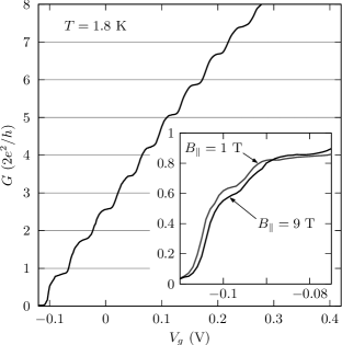

Figure 1 presents the conductance as a function of the gate voltage obtained at zero source-drain bias. The quantized conductance plateaux are observed, which correspond to the successive population/depopulation of the 1D electric subbands. However, the height of particular steps deviates from the quantised values, , where is an integer corresponding to the number of occupied subbands. We find from our four terminal measurements that the perfect quantisation cannot be recovered by subtracting a series resistance. Some authors have considered the influence of electron-electron interactions in 1D systems on conductance quantisation but the prevailing view is that a reduction in plateaux heights results from elastic backscattering, occurring within the disordered quantum channel Kramer et al. (1990); Tekman and Ciraci (1991). We conclude, therefore, that in our wire is diminished by backscattering, , where is the transmission probability similar for each channel up to .
However, the disorder not only reduces uniformly the conductance magnitude but also results in the appearance of conductance resonances at sufficiently low temperatures, which originate from interference of scattering amplitudes. The coexistence of these two effects was already observed experimentally in quasi-ballistic quantum wires Wróbel et al. (1992, 1998); Liang et al. (1999) and is also present for the device studied here. Figure 2 shows conductance measured at various temperature in the He-4 cryostat and the dilution refrigerator. With lowering temperature, the Ramsauer-like resonances clearly show up. This pattern undergoes a change when the sample is warmed-up and cooled-down again, as scattering centres move or change their charge state Tekman and Ciraci (1991). We conclude, therefore, that our sample is indeed in the quasi-ballistic regime, .

The important aspect of our findings is that despite the strong effects of disorder, the anomalous ”0.7” conductance step is visible on the the plateau. In our case it assumes the value of . As expected, when the in-plane magnetic field is applied, the height of this additional plateau decreases, as shown in the inset to fig. 1.
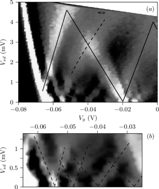
A question arises, whether the conductance step in question is not a resonance peak persisting up 2 K. In order to address this issue, we have carried out dynamic conductance measurements as a function of source-drain bias Patel et al. (1991), as it is known that the ”0.7” plateau becomes even wider for non-zero bias and can survive up to meV Kristensen et al. (2000); de Picciotto et al. (2004). Figure 3 shows the evolution of differential conductance with the bias and gate voltage. Quantized plateaux are visible as collections of lines, which for meV group again to form a “half-integer” plateaux, when the left- and right- moving electrons occupy different consecutive energy levels. For the aggregation of lines is identified as the “0.6” anomaly, discernible also for non-zero biases. The distinction between the additional plateau and any interference effect is evidenced in Fig 4, where the transconductance at K is shown as a function of gate voltage and bias. Together with the distinctively diamond-shaped regions, bordered by high transconductance (bright) areas, also the additional bright strip which crosses the borderline between integer and half-integer conductance diamonds is clearly visible. According to previous studies such characteristic high transconductance line forms when the “0.7-0.5” plateau evolves toward the normal one and it is observed up to biases comparable with the energy gap between levels. Therefore we conclude that the “0.6” anomaly is present also at low temperatures, provided mV. In Fig 4(a) the anomalous plateau is visible as a darker region on the left side of dashed curve. At low source-drain voltages, however, the anomaly is masked by transmission resonances which show-up due to the presence of disorder. As a result, the characteristic high transconductance line is replaced by the “sub-diamond” pattern, which forms because the interference pattern splits in energy. Distinct branches for electrons injected from left and right are marked with dashed lines in Fig 4(b).
Recently, Bielejec Bielejec (2003) et. al. have reported a reduction of the conductance step (down to ) and the presence of ”0.7” anomaly for a long and very high mobility split-gate device. However, no Ramsauer-like transmission resonances were found at low temperatures. For the data reported here, we can observe a stronger reduction of conductance, the ”0.6” anomaly, and transmission resonances. It seems that the wires patterned by shallow etching are well suited for such studies because the 1D confining potential is much stronger comparing to split-gate devices Kristensen et al. (2000); M Knop and Wieck (2005). From the source-drain bias spectroscopy we obtained meV, where is the -th level energy. Assuming a parabolic confinement we estimate the physical width of the device as m (for ). As expected for such a high aspect ratio, we have not observed any zero bias anomaly at 25 mK, which in Fig 4(a) should manifest itself as an additional white spot for and V. The data for low biases are, however, obscured by the presence of transmission resonances, so this conclusion requires further studies.

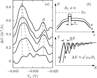
If the interference pattern splits when left- and right-moving electrons start to differ in energy, we may ask if the Zeeman splitting induced by the external field, will lead to a similar effect. Actually, the influence of spin splitting upon mesoscopic conductance fluctuations was observed for diffusive transport in quantum wires of diluted magnetic semiconductor (Cd,Mn)Te:In Jaroszyński et al. (1996). It was found that the correlation field of the universal conductance fluctuations scales with the exchange spin splitting of the conduction band. Therefore we expect that in non-magnetic materials the interference pattern will also split at a sufficiently high in-plane magnetic field - when the Zeeman energy exceeds the separation of fringes. Relevant data for our sample is presented in Fig. 5 where the evolution with the magnetic field of the first two conductance steps is shown.
As seen, a different behaviour for and plateaux is observed. In particular, in the region where transmission resonances do not split – the amplitude of fluctuations and the number of peaks is approximately constant. On the contrary, when the interference pattern changes, as it is shown more clearly in Fig. 6(a), where only the fluctuating part of the total conductance is shown. The amplitude of the two most prominent peaks and decrease and they clearly split at T. We note that this behaviour is consistent with the models of the ”0.7” anomaly, which assume the presence of spontaneous spin polarisation at low carrier densities. If only one spin sublevel is occupied below the plateau, we do not expect any significant changes of the interference pattern with the magnetic field, as indeed observed in the experiment. If, however, both spin channels participate in charge transport, the Zeeman effect should split the Ramsauer resonances, as explained schematically in Fig. 6(b). Furthermore, such splitting should depend only weakly on the exact shape of the potential barrier introduced by disorder, so that , where is the effective Landé factor and is the Bohr magneton. From Fig. 6 we obtained that the splitting , which is more clearly visible for the peak , approaches 4 meV for T. It corresponds to meV, as can determined with the application of source-drain bias spectroscopy data. Thus, the magnetic field evolution of transmission resonances can be applied to the determination of the factor of 1D systems, which is expected to be enhanced by the exchange interaction Thomas et al. (1998); Graham et al. (2003). For our sample we obtained (as compared to 0.44 in bulk GaAs), which is in very good agreement with recent data for ballistic QPCs Koop et al. (2007). The advantage of the proposed method is that it can be applied for long, quasi-ballistic quantum wires. The disadvantage is, of course, the non-reproducibility of observed interference pattern, which changes after subsequent warming up and then cooling down.
In summary, we studied the conductance quantization of quasi-ballistic (), the large aspect ratio () quantum wire. Due to the disorder present in our sample, we observed reduced conductance steps () and transmission resonances on the onset of quantized plateaux, caused by the interference of incoming and reflected electron waves. With the application of source-drain bias spectroscopy, we showed, that the backscattering of electron waves and reduction of transmission probability through the sample do not destroy the existence of so the called 0.7 (in our case 0.6) anomaly. The additional conductance plateau was clearly observed in the temperature range from 1.8 to 0.025 K. Furthermore, we proposed the single electron effect (splitting of the interference peaks with in-plane magnetic field) as a suitable tool for studying the enhancement of electron g-factor in quantum wires which is a collective phenomenon, observed before for ballistic point contacts.
Acknowledgements.
We acknowledge support by the Eurocores/ESF grant SPINTRA (ERAS-CT-2003-980409) and Semiconductor Spintronics ERATO project by JST.References
- Thomas et al. (1996) K. J. Thomas, J. T. Nicholls, M. Y. Simmons, M. Pepper, D. R. Mace, and D. A. Ritchie, Phys. Rev. Lett. 77, 135 (1996).
- Thomas et al. (1998) K. J. Thomas, J. T. Nicholls, N. J. Appleyard, M. Y. Simmons, M. Pepper, D. R. Mace, W. R. Tribe, and D. A. Ritchie, Phys. Rev. B 58, 4846 (1998).
- Cronenwett et al. (2002) S. M. Cronenwett, H. J. Lynch, D. Goldhaber-Gordon, L. P. Kouwenhoven, C. M. Marcus, K. Hirose, N. S. Wingreen, and V. Umansky, Phys. Rev. Lett. 88, 226805 (2002).
- Graham et al. (2003) A. C. Graham, K. J. Thomas, M. Pepper, N. R. Cooper, M. Y. Simmons, and D. A. Ritchie, Phys. Rev. Lett. 91, 136404 (2003).
- Chou et al. (2005) H. T. Chou, S. Luscher, D. Goldhaber-Gordon, M. J. Manfra, A. M. Sergent, K. W. West, and R. J. Molnar, Appl. Phys. Lett. 86, 073108 (2005).
- Koop et al. (2007) E. Koop, A. I. Lerescu, J. Liu, B. J. van Wees, D. Reuter, A. D. Wieck, and C. H. van der Wal, arXiv:0706.0792 (2007).
- Wang and Berggren (1996) C.-K. Wang and K.-F. Berggren, Phys. Rev. B 54, R14257 (1996).
- Rokhinson et al. (2006) L. P. Rokhinson, L. N. Pfeiffer, and K. W. West, Phys. Rev. Lett. 96, 156602 (pages 4) (2006).
- DiCarlo et al. (2006) L. DiCarlo, Y. Zhang, D. T. McClure, D. J. Reilly, C. M. Marcus, L. N. Pfeiffer, and K. W. West, Phys. Rev. Lett. 97, 036810 (pages 4) (2006).
- Meir et al. (2002) Y. Meir, K. Hirose, and N. S. Wingreen, Phys. Rev. Lett. 89, 196802 (2002).
- Kristensen et al. (2000) A. Kristensen, H. Bruus, A. E. Hansen, J. B. Jensen, P. E. Lindelof, C. J. Marckmann, J. Nygård, C. B. Sørensen, F. Beuscher, A. Forchel, et al., Phys. Rev. B 62, 10950 (2000).
- Graham et al. (2007) A. C. Graham, D. L. Sawkey, M. Pepper, M. Y. Simmons, and D. A. Ritchie, Phys. Rev. B 75, 035331 (pages 6) (2007).
- Reilly et al. (2001) D. J. Reilly, G. R. Facer, A. S. Dzurak, B. E. Kane, R. G. Clark, P. J. Stiles, R. G. Clark, A. R. Hamilton, J. L. O’Brien, N. E. Lumpkin, et al., Phys. Rev. B 63, 121311 (2001).
- de Picciotto et al. (2004) R. de Picciotto, L. N. Pfeiffer, K. W. Baldwin, and K. W. West, Phys. Rev. Lett. 92, 036805 (pages 4) (2004).
- M Knop and Wieck (2005) R. M. U. W. U. K. D. R. C. R. M Knop, M Richter and A. D. Wieck, Semicond. Sci. Technol. 20, 814 (2005).
- Kramer et al. (1990) B. Kramer, J. Mas̆ek, V. S̆pic̆ka, and B. Velický, Surf. Sci. 229, 316 (1990).
- Tekman and Ciraci (1991) E. Tekman and S. Ciraci, Phys. Rev. B 43, 7145 (1991).
- Wróbel et al. (1992) J. Wróbel, F. Kuchar, K. Ismail, K. Y. Lee, H. Nickel, and W. Schlapp, Surf. Sci. 263, 261 (1992).
- Wróbel et al. (1998) J. Wróbel, T. Dietl, K. Regiński, and M. Bugajski, Phys. Rev. B 58, 16252 (1998).
- Liang et al. (1999) C.-T. Liang, M. Y. Simmons, C. G. Smith, D. A. Ritchie, and M. Pepper, Appl. Phys. Lett. 75, 2975 (1999).
- Patel et al. (1991) N. K. Patel, J. T. Nicholls, L. Martn-Moreno, M. Pepper, J. E. F. Frost, D. A. Ritchie, and G. A. C. Jones, Phys. Rev. B 44, 10973 (1991).
- Bielejec (2003) J. L. M. S. J. R. J. Bielejec, E.; Seamons, Superlattices Microstruct. 34, 493 (2003).
- Jaroszyński et al. (1996) J. Jaroszyński, J. Wróbel, M. Sawicki, E. Kamińska, T. Skośkiewicz, G. Karczewski, T. Wojtowicz, A. Piotrowska, J. Kossut, and T. Dietl, Phys. Rev. Lett. 76, 1556 (1996).