Two-dimensional imaging of the spin-orbit effective magnetic field
Abstract
We report on spatially resolved measurements of the spin-orbit effective magnetic field in a GaAs/InGaAs quantum-well. Biased gate electrodes lead to an electric-field distribution in which the quantum-well electrons move according to the local orientation and magnitude of the electric field. This motion induces Rashba and Dresselhaus effective magnetic fields. The projection of the sum of these fields onto an external magnetic field is monitored locally by measuring the electron spin-precession frequency using time-resolved Faraday rotation. A comparison with simulations shows good agreement with the experimental data.
In the reference frame of a moving electron, electric fields transform into magnetic fields, which interact with the electron spin and couple it to the electron’s orbital motion, leading to spin-orbit (SO) interaction. In crystals lacking an inversion center such as GaAs, effective magnetic fields due to bulk inversion asymmetry (BIA) were predicted by Dresselhaus Dresselhaus (1955). In heterostructures, structure inversion asymmetry (SIA) leads to an effective magnetic field called Rashba term Bychkov and Rashba (1984). Both contributions have been studied extensively (for a review, see Ref. Winkler (2003)) and are thought to play a crucial role in future spintronic devices, because the coupling of the orbital and the spin degrees of freedom opens a new way to spin manipulation, for example by flipping spins with oscillating electric fields Rashba and Efros (2003a, b); Duckheim and Loss (2006); Golovach et al. (2006). The interplay between Dresselhaus and Rashba SO interaction has been studied Duckheim and Loss (2007); Bernevig et al. (2006) and proposed for use in a spin transistor Schliemann et al. (2003). For finite electron wave numbers, SO interaction leads to a spin splitting at zero external magnetic field, which is observable as a beating of Shubnikov-de Haas oscillations Das et al. (1989); Luo et al. (1990); Engels et al. (1997); Schapers et al. (1998); Hu et al. (1999); Pfeffer and Zawadzki (1999); Brosig et al. (1999) and can be used to experimentally determine the strength of the total SO interaction. The zero-field spin splitting also results in a spin-selective momentum scattering and can lead to spin-dependent photocurrents Ganichev et al. (2004), which allow the determination of the ratio between the Rashba and Dresselhaus contributions by studying their directional dependence. Since SO interaction is the main reason for spin relaxation in GaAs quantum well (QW) samples, the directional dependence of spin relaxation reveals the relative strength of the Rashba and Dresselhaus terms Averkiev et al. (2006). A more direct method to get access to the SO fields is to impose a drift momentum on the conduction-band electrons by applying an in-plane electric field. This leads to two different effects: In a steady-state situation, the spins are oriented along the SO field Edelstein (1990); Aronov et al. (1991); Kato et al. (2004a); Silov et al. (2004). If the spins of an ensemble of such drifting electrons are polarized by means of an optical pump pulse, a coherent spin precession about the SO field takes place, which has been observed using time-resolved Faraday rotation (TRFR) in a bulk GaAs epilayer Kato et al. (2004). Using TRFR, we have recently shown that the absolute values of both the Rashba and the Dresselhaus field can be determined in a two-dimensional electron gas by studying the precession frequency of electron spins as a function of the electron’s direction of motion with respect to the crystal lattice Meier et al. (2007). An oscillating electric field was applied at an arbitrary direction in the plane of an InGaAs quantum well (QW) using two pairs of opposed electric gates arranged perpendicularly to each other and enclosing a square area of QW electrons [see Fig. 1(a)].
Here, we study the spatial distribution of the total SO effective magnetic field between and outside the four gate electrodes that are used to generate the in-plane electric field. We show that the measured maps of spin-precession frequency can be well explained by assuming that the electrons move along the spatially varying electric field and that their spins perceive a SO effective magnetic field given by their local drift momentum. Depending on the orientation of an external magnetic field with respect to the crystal axis, the precession frequency becomes sensitive to drift momentum along a fixed in-plane direction, allowing to spatially map the corresponding momentum component. A simulation with fixed values for the Rashba and Dresselhaus coefficients as determined in Ref. Meier et al. (2007) leads to good agreement with the measured precession-frequency maps. Specifically, the results confirm that the electron drift momentum in the center of the gates can be described by the superposition of two perpendicular components given by the two orthogonal gate biases, as it was assumed in Ref. Meier et al. (2007). Away from the center, however, the electric field and thus the spin-precession frequency start to vary. Large SO-induced effects on the spin-precession frequency can still be detected far away from the region between the gates, because of the connection lines to the gates. This illustrates the importance of a precise definition of the electrical connection scheme in a larger set-up and the difficulty of applying electric fields only at given positions of a two-dimensional electron gas.
The samples are either a 20- or 43-nm-wide InGaAs/GaAs QW as described in Ref. Meier et al. (2007) (sample 1 and 2). We experimentally determine by measuring the electron spin-precession frequency of optically excited conduction-band electrons using scanning TRFR ( denotes Planck’s constant, the electron -factor, and the Bohr magneton). With a first, circularly polarized pump pulse tuned to the absorption edge of the QW ( nm, average power W, pulse width of 2 ps, and repetition rate of 80 MHz), we create a spin polarization in the QW conduction band perpendicular to the QW plane. A pump-probe delay time later, we probe the spin polarization with a linearly polarized probe pulse (average power W) and monitor the rotation angle of its polarization plane. This Faraday rotation angle can be fit to to yield both the spin-precession frequency and the spin-coherence time . By spatially moving the sample relative to the laser beams, the spin dynamics can be studied with a spatial resolution limited by the diameter of the beam in the focus, here approximately 15 m. Scanning Kerr microscopy has been used in Refs. Stephens et al. (2003) for spatially resolving nuclear imprinting effects and in Refs Crooker and Smith (2005); Crooker et al. (2005) for studying spin transport in GaAs epilayers.
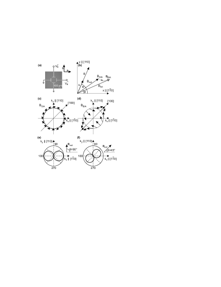
On top of the sample, four gates and the corresponding connection lines were defined using standard electron-beam lithography, evaporation of a 10-nm-thick Ti adhesion layer and a 80-nm-thick Au layer, and lift-off techniques. As shown in Fig. 1(a), opposite gate-pairs were connected to phase-locked oscillators, one each for the two perpendicular directions and . Two neighboring gates were grounded, and by adjusting the voltage amplitudes and on the other two gates, an oscillating electric field , MHz, is induced in the QW plane. In the center of the four electrodes, points at an angle, with respect to the -axis, given by . We have fabricated different samples in which the -axis is oriented along either or of the semiconductor crystal. We define a coordinate system with and , and label the angle of with the -axis as , see Fig. 1(b). As long as is large compared to the mean collision time of the electrons in the QW ( ps), the electrons adiabatically follow and their drift wave vector is given by , with the effective electron mass and the electron mobility. Furthermore, the small collision time prevents the electrons from leaving the laser focus during the time . Because of their non-vanishing -vector, the electrons are subject to SO effective magnetic fields, which in two-dimensional systems are given by Ganichev and Prettl (2003); Winkler (2003)
| (1) |
with and and the Rashba and Dresselhaus coupling constants, respectively. The geometrical dependence on is shown in Fig. 1(c) and (d). Whereas is always perpendicular to , points along for the and directions. When analyzing the spin precession, both SO contributions can be added to an external magnetic field Kalevich and Korenev (1990); Engel et al. (2007), which we apply in the plane of the QW and at an angle with the -axis, as illustrated in Fig. 1(b). For all data presented, we choose T.
If , , the total magnetic field can be expressed by Meier et al. (2007)
| (2) |
Here, is the time delay between the electric-field oscillation and the pump pulse (known up to an offset , which is constant in all experiments), and
| (3) |
By probing at different times , we find to oscillate with with the frequency . Figure 2(a) shows TRFR scans for two different . This data is obtained on sample 1 in the center of the four gates that are aligned with the - and -axis. With = 1 V, the electric field is oriented along at the position of the laser focus. is applied along () . The TRFR signal monitors the coherent precession of the QW electron spins about the total field . Spins precess faster for = -1.4 ns than for = 1.7 ns. This variation of the precession frequency follows the oscillation of , as becomes evident when plotting the fitted spin precession frequency as a function of , see symbols in Fig. 2(b). The data points fit to a sinusoidal oscillation at frequency = 160 MHz (solid line). Except from a much weaker contribution at Meier et al. (2007), we do not observe higher harmonics in , from which we conclude that the linear dependence of the effective spin-orbit magnetic field on in Eq. 1 is valid. Specifically, terms cubic in can be neglected. Such terms can be significant for the zero-field SO splitting Miller et al. (2003) at the Fermi wave vector. In our case however, the effective SO magnetic field is determined by the in-plane drift wave vector , which is much smaller than the quantized wave number perpendicular to the QW, and therefore negligible cubic contributions are expected.
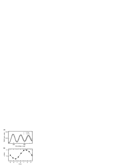
The obtained can be converted into , the amplitude of its oscillation being given by according to Eq. 2. By measuring at varying and in the center of the four gates and comparing to Eq. 3, we determine mT, mT for sample 1, and mT, mT for sample 2. These values were obtained for a gate-modulation amplitude of 2 V, corresponding to V/m Meier et al. (2007).
In a geometrical interpretation, is the projection of onto . Because the SO fields depend linearly on , is proportional to the projection of the local field onto an axis defined by . At constant , a spatial map of therefore directly images one component of . Figure 1(e) and (f) show the calculated using the measured values for and as a function of for and for sample 1. In the first case, is proportional to the projection of onto the -axis, with an amplitude of . For , the projection is onto . For vanishing SIA, the highest visibility would be exactly at .
The electric field is given by a superposition of the electric fields induced by the two pairs of electrodes along the and axis, and can be numerically determined with a partial differential-equation solver (e.g. pdetool in Matlab) with boundary conditions given by the voltages applied to the gate electrodes and their connection lines. Figure 3 shows a situation for sample 1 with the gate electrodes oriented along the - and -axis, and at two different bias configurations, where either the top and the right gate electrode [Fig. 3(a)] or only the right gate electrode [Fig. 3(b)] were set to V, and all other gates were grounded. In the center of the electrodes, points along the -axis () or the -axis (), respectively, as expected from simply superposing two uniform fields along the and axis that are proportional to the two gate biases.
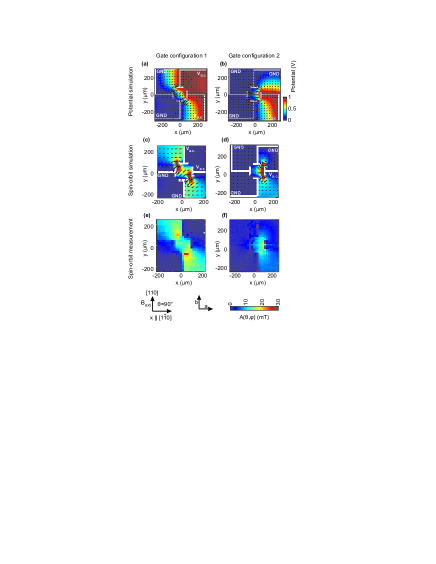
At every point in the two-dimensional sample plane, the local electric field gives rise to a local -vector, which allows the calculation of using Eqs. (1) and (3). The result of this simulation is shown in Fig. 3(c) and (d). Considerable SO fields are also expected away from the four gate electrodes, because of the electric fields induced by the connection lines. The corresponding measurements are shown in Fig. 3(e) and (f). The agreement with the simulation is good, except for the values of measured close to a gate edge that are a factor of lower than in the simulation. There, the simulation assumes perfect edges, leading to very high electric fields. In reality, the edges are rough and round, and the electric field is lower. Moreover, the simulations neglect the fact that the gates are vertically offset from the QW by 30 nm, which compared to their lateral separation of m is, however, a negligible distance.
As expected from Fig. 1(e), electric fields along lead to high SO contributions to . In Figs. 3(c) and (e), the connection lines along induce strong electric fields along in the upper left and the lower right quadrant of the sample. These fields lead to a -vector in -direction, and, as visible from Fig. 1(e), to a high . In contrast, close to the horizontal connection lines along , the high electric fields in -direction do not lead to visible SO fields, as in this situation, is perpendicular to and therefore .
For the situation with three grounded gates [Fig. 3(f)], outside of the four gates the electric field component along is large in the full lower right corner and partially in the upper right corner, leading to a high value of at these positions. Inside the gates, is mainly aligned along and decays from right to left because of the shielding from the upper and lower gates which are at ground potential, which is directly observable in the measured and simulated maps of .
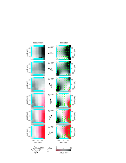
In Fig. 4, we focus on the area between the four gate electrodes. We choose a configuration in which the gates and therefore the )-axis are oriented at to the ()-axis. The measurements were taken on sample 2, and for the simulations the obtained values for and are used. We set , such that is sensitive to the component of approximately along , i.e. along the [100]-axis [see Fig. 1(f)]. The angle of the electric field in the center of the electrodes has been rotated by in each step by varying the amplitudes and of the two phase-locked oscillators, connected to the bottom and the right gate electrode, respectively, with = 1 V. This direction is indicated by an arrow between the measurement (left column) and the simulation (right column). The simulation is again in good agreement with the measurement, except close to edges, where the simulated electric field and therefore also the SO fields are higher than observed.
In this configuration, is sensitive to the horizontal component of , and therefore, the highest are measured close to the right gate electrode (connected to ), provided that is large enough. There, is positive for and (positive ) and negative for and (negative ). As can be seen from the simulations in the right column of Fig 3, the sign of correlates with the component of along . For , the left and right electrodes are grounded, and points along the vertical direction in the center of the gates. On both the left and the right side of the center, turns sideways towards the respective grounded lateral electrode, leading to positive and negative values for on the two sides. Even though the bottom electrode induces strong electric fields, only a small is observed close to the electrode, since the field is mainly oriented along , i.e. perpendicular to . For , has both positive and negative components along close to the right gates, therefore leading to the appearance of both signs of , as can be seen both in the simulation and in the measurement. In the corners of the square defined by the four gate electrodes, high are measured as long as the two neighboring electrodes are on different potentials. There, the electric field is diagonal and therefore has substantial components along .
In conclusion, we have shown that the electric field induced by biased gate electrodes modifies the electron spin precession in an InGaAs QW through the presence of an SO effective magnetic field. Spatially resolved optical measurements of the spin precession frequency are in good agreement with numerically obtained spatial maps. They confirm that the change in spin precession frequency is a measure of the projection of the drift momentum and thus the electric-field along an in-plane direction that is given by the Rashba and Dresselhaus constants as well as the direction of . By adjusting the angle of , different components of the electric field can be spatially mapped. Alternatively, if the electric field is known, this technique might allow to measure spatial variations of the Rashba and Dresselhaus constants Sherman (2003); Liu and Chang (2006).
We acknowledge R. Allenspach, M. Duckheim, T. Ihn, R. Leturcq, D. Loss and M. Witzig for helpful discussions. This work was supported by the Swiss National Science Foundation (NCCR Nanoscale Science).
References
- Dresselhaus (1955) G. Dresselhaus, Phys. Rev. 100, 580 (1955).
- Bychkov and Rashba (1984) Y. A. Bychkov and E. I. Rashba, J. Phys. C 17, 6039 (1984).
- Winkler (2003) R. Winkler, Spin-Orbit Coupling Effects in Two-Dimensional Electron and Hole Systems, vol. 191/2003 of Springer Tracts in Modern Physics (Springer, 2003).
- Rashba and Efros (2003a) E. I. Rashba and A. L. Efros, Phys. Rev. Lett. 91, 126405 (2003a).
- Rashba and Efros (2003b) E. I. Rashba and A. L. Efros, Appl. Phys. Lett. 83, 5295 (2003b).
- Duckheim and Loss (2006) M. Duckheim and D. Loss, Nature Phys. 2, 195 (2006).
- Golovach et al. (2006) V. N. Golovach, M. Borhani, and D. Loss, Phys. Rev. B 74, 165319 (2006).
- Duckheim and Loss (2007) M. Duckheim and D. Loss, Phys. Rev. B 75, 201305 (2007).
- Bernevig et al. (2006) B. A. Bernevig, J. Orenstein, and S.-C. Zhang, Phys. Rev. Lett. 97, 236601 (2006).
- Schliemann et al. (2003) J. Schliemann, J. C. Egues, and D. Loss, Phys. Rev. Lett. 90, 146801 (2003).
- Das et al. (1989) B. Das, D. C. Miller, S. Datta, R. Reifenberger, W. P. Hong, P. K. Bhattacharya, J. Singh, and M. Jaffe, Phys. Rev. B 39, 1411 (1989).
- Luo et al. (1990) J. Luo, H. Munekata, F. F. Fang, and P. J. Stiles, Phys. Rev. B 41, 7685 (1990).
- Engels et al. (1997) G. Engels, J. Lange, T. Schäpers, and H. Lüth, Phys. Rev. B 55, R1958 (1997).
- Schapers et al. (1998) T. Schapers, G. Engels, J. Lange, T. Klocke, M. Hollfelder, and H. Luth, J. Appl. Phys. 83, 4324 (1998).
- Hu et al. (1999) C.-M. Hu, J. Nitta, T. Akazaki, H. Takayanagi, J. Osaka, P. Pfeffer, and W. Zawadzki, Phys. Rev. B 60, 7736 (1999).
- Pfeffer and Zawadzki (1999) P. Pfeffer and W. Zawadzki, Phys. Rev. B 59, R5312 (1999).
- Brosig et al. (1999) S. Brosig, K. Ensslin, R. J. Warburton, C. Nguyen, B. Brar, M. Thomas, and H. Kroemer, Phys. Rev. B 60, R13989 (1999).
- Ganichev et al. (2004) S. D. Ganichev, V. V. Bel’kov, L. E. Golub, E. L. Ivchenko, P. Schneider, S. Giglberger, J. Eroms, J. D. Boeck, G. Borghs, W. Wegscheider, Phys. Rev. Lett. 92, 256601 (2004).
- Averkiev et al. (2006) N. S. Averkiev, L. E. Golub, A. S. Gurevich, V. P. Evtikhiev, V. P. Kochereshko, A. V. Platonov, A. S. Shkolnik, and Y. P. Efimov, Phys. Rev. B 74, 033305 (2006).
- Edelstein (1990) V. M. Edelstein, Solid State Comm. 73, 233 (1990).
- Aronov et al. (1991) A. G. Aronov, Y. B. Lyanda-Geller, and G. E. Pikus, Soviet Physics - JETP 73, 537 (1991).
- Kato et al. (2004a) Y. K. Kato, R. C. Myers, A. C. Gossard, and D. D. Awschalom, Phys. Rev. Lett. 93, 176601 (2004a).
- Silov et al. (2004) A. Y. Silov, P. A. Blajnov, J. H. Wolter, R. Hey, K. H. Ploog, and N. S. Averkiev, Appl. Phys. Lett. 85, 5929 (2004).
- Kato et al. (2004) Y. Kato, R. C. Myers, A. C. Gossard, and D. D. Awschalom, Nature 427, 50 (2004).
- Meier et al. (2007) L. Meier, G. Salis, I. Shorubalko, E. Gini, S. Schön, and K. Ensslin, Nature Phys. 3,650 (2007).
- Stephens et al. (2003) J. Stephens, R. K. Kawakami, J. Berezovsky, M. Hanson, D. P. Shepherd, A. C. Gossard, and D. D. Awschalom, Phys. Rev. B 68, 041307 (2003).
- Crooker and Smith (2005) S. A. Crooker and D. L. Smith, Phys. Rev. Lett. 94, 236601 (2005).
- Crooker et al. (2005) S. A. Crooker, M. Furis, X. Lou, C. Adelmann, D. L. Smith, C. J. Palmstrm, and P. A. Crowell, Science 309, 2191 (2005).
- Ganichev and Prettl (2003) S. Ganichev and W. Prettl, Journal of Physics: Condensed Matter 15, R935 (2003).
- Engel et al. (2007) H.-A. Engel, E. I. Rashba, and B. I. Halperin, Phys. Rev. Lett. 98, 036602 (2007).
- Kalevich and Korenev (1990) V. Kalevich and V. Korenev, JETP Lett. 52, 230 (1990).
- Miller et al. (2003) J. B. Miller, D. M. Zumbühl, C. M. Marcus, Y. B. Lyanda-Geller, D. Goldhaber-Gordon, K. Campman, and A. C. Gossard, Phys. Rev. Lett. 90, 076807 (2003).
- Sherman (2003) E. Y. Sherman, Appl. Phys. Lett. 82, 209 (2003).
- Liu and Chang (2006) M.-H. Liu and C.-R. Chang, Phys. Rev. B 74, 195314 (2006).