Tunneling Study of the Charge-Ordering Gap on the Surface of La0.350Pr0.275Ca0.375MnO3 Thin Films
Abstract
Variable temperature scanning tunneling microscopy/spectroscopy studies on (110) oriented epitaxial thin films of La0.350Pr0.275Ca0.375MnO3 are reported in the temperature range of 77 to 340 K. The films, grown on lattice matched NdGaO3 substrates, show a hysteretic metal-insulator transition in resistivity at 170 K. The topographic STM images show step-terrace morphology while the conductance images display a nearly homogeneous surface. The normalized conductance spectra at low temperatures (T150 K) show an energy gap of 0.5 eV while for T180 K a gap of 0.16 eV is found from the activated behavior of the zero bias conductance. The presence of energy gap and the absence of phase separation on the surface over more than 2 m2 m area contradicts the metallic behavior seen in resistivity measurements at low temperatures. We discuss the measured energy gap in terms of the stabilization of the insulating CO phase at the film surface.
The research over past decade on colossal magneto-resistive (CMR) manganites book-rao-raveau ; salamon-jaime ; von-helmolt has led to a number of very interesting phenomena. These are now understood to be systems with strongly coupled charge, spin, lattice, and orbital degrees of freedom with a number of possible phases of nearly equal free energies dagotto-rev ; salamon-jaime ; ahn . These phases are thought to coexist in some manganite compositions and the relative fractions of phase are sensitive to external perturbations such as magnetic field, electric field, pressure, and strain. In fact, a sudden termination of the periodic potential at the surface is a perturbation that seems to make the surface quite different from the bulk freeland-plummer . The bulk of some of the small band-width manganites hwang-batlogg undergoes an electronic phase-separation uehara-cheong ; kim-cheong into metallic and insulating regions, which is thought dagotto-rev ; moreo ; ahn to be responsible for the CMR effect. Various research groups have observed multiple phases in some of the manganites, in particular, in (La1-xPrx)0.625Ca0.375MnO3 series, using different probes uehara-cheong ; zhang-lozanne ; lee including Scanning Tunneling Microscopy / Spectroscopy (STM/S) fath ; renner-cheong ; becker ; moshnyaga . However, the detailed electronic nature of the individual phases is far from understood salamon-jaime .
In this work, we have probed the surface of a relatively narrow band-width hole-doped manganite La0.350Pr0.275Ca0.375MnO3 (LPCMO), using the STM/S in the temperature range of 77K to 340K. The ground state of the two end members of this compound La0.675Ca0.375MnO3 and Pr0.675Ca0.375MnO3 are ferromagnetic metal and antiferromagnetic charge-ordered (CO) insulator, respectively. Intermediate compositions show a CO transition around 200 K with coexisting CO insulating and charge-disordered conducting phases uehara-cheong . Our main objective in this study has been to probe various phases in LPCMO films by local tunneling spectroscopy to understand their nature and contribution to CMR. However, we find that the low energy part of the spectra evolves quite homogeneously with temperature with an energy gap that changes from 0.16 eV to 0.5 eV on cooling. Whilst the gap varies slightly on a nanometer length scale, it exists even below the insulator-metal transition temperature () measured by resistivity. This is the first temperature dependent STM/S study on this narrow bandwidth manganite, and our major finding is the persistence of a nearly homogeneous CO gap which we interpret in terms of the stabilization of the CO phase on the surface even though the bulk of the film shows a phase separated behavior.
Epitaxial films of thickness 200 nm of LPCMO were grown at a deposition rate of 0.3 nm/s on (110) surface of NdGaO3 (NGO) single crystals by using pulsed laser deposition (PLD). The (110) direction refers to the orthorhombic unit cell of NGO with d110 = 0.38595 nm. A KrF excimer laser


operated at 10 Hz with an areal energy density of 2 Jcm-2/pulse on the surface of a stoichiometric sintered target of LPCMO. For these films we find a step-terrace morphology for relatively slow growth conditions while the faster growth rates lead to a granular surface. In this paper, we focus on the STM/S study of LPCMO thin films with step-terrace surface morphology. Films with granular morphology have an associated electronic inhomogeneity and they may not reflect the film’s intrinsic electronic behavior. For resistivity measurements, silver contact pads were deposited through a shadow mask in a four probe configuration. The STM/S measurements were performed using a homemade variable temperature STM with fresh cut Pt0.8Ir0.2 wire tip. The STM head is based on a design published elsewhere anjan-stm while the electronics and software are commercial. The STM measurements reported here have been carried out in liquid nitrogen in 77 - 340 K temperature range in a cryogenic vacuum. After transferring the sample to the STM in air, the cryostat is pumped and flushed with He-gas a few times. The sample transfer is carried out quite fast so that the sample is exposed to air for less than 30 min. Finally the cryostat is pumped to a high vacuum (110-4 mbar) prior to cooling in liquid nitrogen. To ensure a clean sample surface we heat the whole STM to 340K for a few hours keeping the surroundings at liquid nitrogen temperatures.
The standard ac-modulation technique was used for STS and conductance spectra with a modulation amplitude between 30 and 50 mV. The dc-component of current, , is fed to the z-feedback for controlling and measuring the tip-sample separation while a lock-in amplifier measured the ac-component giving the conductance, dI/dV, at bias V. Simultaneous conductance and topographic images in constant-current mode at a bias (V=) are obtained by measuring the lock-in output and the z-feedback voltage, respectively, over the surface. In this mode, the feedback, by varying tip-sample separation, ensures that the integrated conductance up to is the same at all points of the image. As a result, in the dark regions of a conductance image the current gets less contribution from the conductance at larger bias and more contribution from the small bias. Thus, in a conductance image, the darker regions represent more metallic (or less gapped) areas renner-book-ch and the topographic and conductance images are anti-correlated for flat surfaces.
The four probe resistance as a function of temperature for an LPCMO film (Fig.1a) shows an insulator-metal transition at TMI = 170 K with more than two orders of magnitude change in resistivity, which is typical of the narrow bandwidth CMR manganites wu-greene-millis . The cooling and heating curves differ slightly near the transition indicating the presence of more than one phase in the bulk of this film as shown in the inset of Fig.1a. Resistivity in LPCMO single crystals and polycrystalline samples shows a small feature at 200 K due to opening of a CO gap uehara-cheong ; lee , which is absent in thin films Tara Dhakal ; W. Prellier . This could be due to the small substrate induced strain effect making the CO transition not so sharp with respect to temperature. The formation of charge ordered state below 210 K in the same composition thin films on NGO substrate has been observed by electron microscopy and diffraction studies by Chaudhuri, et. al.Chaudhuri . In Fig.1b, we plot ln() Vs 1/T for 170 KT285 K, which establishes the activated behavior of resistivity with an activation energy () of 0.12 eV. This is in close agreement with the average optical gap (2) of about 0.2 eV in this temperature range observed by Lee et.al. lee in LPCMO single crystals of slightly different composition.
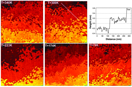
The STM topographic images of the LPCMO film (in Fig.2) between 340 and 78 K temperature show step-terrace morphology with a terrace width of about 200 nm. The rms roughness of each terrace is found to be less than 0.1 nm. From the conductance images, as discussed later, some of this roughness can be attributed to the electronic inhomogeneities. The terrace boundaries are quite irregular together with a few isolated islands of lateral size up to ten nanometers. From the line-cut shown in Fig.2c, the height of the terrace is found to be 0.4 (0.05) nm in agreement with the step height of 0.38 nm for (110) planes of LPCMO. Further, a tiny (0.2%) epitaxial mismatch between the NGO substrate and the LPCMO films for such large thickness would not leave significant strain near the surface. The presence of such smooth terraces allows local tunneling experiments in the regions that are unaffected by the presence of steps or grain boundaries and their associated local disorders and non-uniformities.
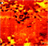
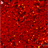
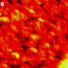
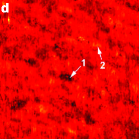

Fig.3 shows a set of simultaneously taken topographic and conductance images at 140 K. As discussed earlier, the bright regions of a conductance image represent more gapped areas. The conductance images have some very bright spots of about 5 nm size with a relatively low coverage ( 20 spots/). The image in Fig.3b has a number of these bright spots. These spots are seen at all temperatures and they have a large energy gap (1 to 1.5 eV) as found from the local spectra. It is possible that these are either second phase materials belonging to the parent compounds, which are all antiferromagnetic insulators, or oxides of the constituent metals. Since their fraction is very small it is difficult to detect them in X-ray diffraction. Such defects are also not seen in high resolution TEM images of similar samples, which makes us believe that they are segregated at the surface.
Other than these large-gap-spots, a weak contrast in the conductance images (Fig.3d) is also seen at nanometer length scale, which is somewhat anti-correlated with the contrast of the simultaneous topographic image. The image in Fig.3d is a smaller area image of region without any bright spots as discussed above. The cross-correlation coefficient between the topographic and conductance images on terraces is found to be -0.2 showing that the density of states (DOS) inhomogeneity is partly responsible for the topographic contrast. The detailed tunneling spectra, with two representative ones in Fig.3e, show that this inhomogeneity actually corresponds to a small variation in the CO-gap value. Similar inhomogeneity is seen at all temperatures from 77 to 340 K. We believe that this electronic contrast represents some frozen chemical inhomogeneity in this non-stoichiometric compound.


A tunneling spectrum, other than the DOS, is also affected by finite temperatures and the voltage dependence of the tunneling matrix element wolf ; stroscio-feenstra . The temperature smears out the spectral features of width less than a few . The voltage dependence of the matrix element is more difficult to handle for large bias spectra as one does not know much about the details of the tunnel barrier. In general, one has to be careful in comparing the absolute dI/dV values at a given bias for two spectra that have different behavior with V as it is difficult to ensure the same tunneling matrix element for the two spectra. For such comparisons we have chosen the spectra with same junction resistances at a fixed bias. To extract the DOS from a dI/dV spectra a widely used method stroscio-feenstra is to plot (dI/dV)/(I/V) (or d(lnI)/d(lnV)), which normalizes away the voltage dependence of the matrix element from the spectra. Practically, d(lnI)/d(lnV) sharpens the spectral features that are not smeared away by temperature.
Temperature dependence of the tunneling spectra is shown in Fig.4a with each spectrum taken at a tunnel current set-point of 0.1 nA at 1 V bias. The conductance near zero bias at low temperatures is nearly flat with a very small magnitude indicating the presence of a gap while that at higher temperatures has a noticeable curvature with significant conductance value. This indicates opening of an energy gap with cooling. The low temperature gap is more clearly visible in dlnI/dlnV-V plots in Fig.4b. We also show two representative I-V spectra in the inset of Fig.4a. The gap value (2) at low temperatures is found to be 0.5(0.1) eV from the separation between the center of the two gap edges in dlnI/dlnV spectra (Fig.4b). This is in reasonable agreement with the low temperature gap of 0.38 eV found in optical measurements of Lee et.al. lee . As mentioned earlier, this gap value has small ( 0.1 eV) variations over a few nanometer length scale but the spectra are qualitatively homogeneous. To look for the phase separation, we have studied the spectra over reasonably large areas (2 m2 m) with step-terrace morphology without any signature of non-gapped spectra at low temperatures. We have also thermally cycled this sample several times but this behavior remains unchanged.

At higher temperatures, the zero bias conductance (ZBC), , is found to show an activated behavior indicative of the presence of a smaller gap that is thermally smeared out. Ln() above 180 K is plotted in Fig.5 with respect to 1/T. The linear fit shown in the same figure gives an activation gap () of 0.08 eV.
Phase separation into a charge ordered insulating and a charge disordered conducting phase on sub-micron scale is well established in LPCMO bulk as well as thin films. This is also apparent in thin films studied here from the hysteretic behavior of resistivity. The charge-order exists in LPCMO both below and above kiryukhin-jeong with a change in the CO fraction with temperature and magnetic field uehara-cheong . The insulating behavior above of the LPCMO films studied here can be attributed to the presence of the CO phase. We found an energy gap () above of magnitude 0.12 eV from the resistivity measurements while the gap found from the ZBC of the tunneling spectra is 0.08 eV. These two are consistent with each other given that one probes the surface while the other probes the bulk of the film. An energy gap (2) of 0.5 eV below is found from dlnI/dlnV spectra. Both these gaps agree reasonably well with those observed by optical spectroscopy lee .
The tunneling measurements above agree with the bulk resistivity but the two show quite opposite behavior at low temperatures. It is impossible to get such conducting behavior in bulk at low temperatures with such a pronounced gap in the electronic DOS in this three dimensional compound. This result is extremely puzzling and the only reconciliation we can think of is that the tunneling somehow is not probing the bulk properties of the film. Surface contamination is the first thing to blame and we cannot rule this out completely as we do expose our samples to air but for a very short time while transferring them from the growth chamber to the STM. However, excellent terraces over large areas and a good correlation of the temperature dependent tunneling data with charge-ordering makes us strongly believe that we are probing intrinsic properties of the surface of the films, which has a charge-ordered phase stabilized.
The X-ray spectroscopy and spin polarized tunneling studies on manganites freeland-plummer also show that the surface layer is insulating with significant suppression in ferromagnetism. The surface is also found to be different from the bulk from the NMR studies on polycrystalline manganites bibes . In LPCMO, this effect could be quite strong as it is a three dimensional compound. So it is reasonable to assert that a sudden termination of the lattice stabilizes a charge-ordered insulating phase on the surface. Surface reconstruction or a different chemical composition of the film, particularly oxygen stoichiometry, near the surface are the two possibilities that we can speculate. Nevertheless, this seems to be an intrinsic feature of manganites and it will play a significant role in polycrystalline samples grain-tunneling ; sudheendra-rao and devices utilizing the spin-polarization planar-junction of the surface electrons.
In conclusion, our STM/S studies on epitaxial La0.350Pr0.275Ca0.375MnO3 films on NdGaO3 substrate show a temperature dependent energy gap. Conductance images show some inhomogeneity on nanometer length scale; however, no sign of any metallic phase was found in the tunneling spectra for TTMI. The low temperature gap seen here is inconsistent with the resistivity measurements which shows a metallic behavior below TMI. From the correlation of the energy gap with the CO phase we conclude that a charge-ordered insulating phase remains stabilized near the surface, which masks the signatures of the phase separation in the bulk of the film.
I Acknowledgements
URS acknowledges financial support from CSIR, AKG acknowledges a research grant from DST of the Govt. of India. S. Rajauria’s contribution to the initial work on the STM set-up is acknowledged.
References
- (1) :
- (2) CMR, Charge Ordering and Related Properties of Manganese Oxides, ed. by C. N. R. Rao and B. Raveau (World Scientific, Singapore, 1998).
- (3) M. B. Salamon and M. Jaime, Rev. Mod. Phys. 73, 583 (2001); M. Imada, A. Fujimori, and Y. Tokura, Rev. Mod. Phys. 70, 1039 (1998).
- (4) R. von Helmolt, J. Wecker, B. Holzapfel, L. Schultz, and K. Samwer, Phys. Rev. Lett. 71, 2331 (1993);
- (5) E. Dagotto, T. Hotta, and A. Moreo, Phys. Rep. 344, 1 (2001).
- (6) K. H. Ahn T. Lookman, and A. R. Bishop, Nature 428, 401 (2004).
- (7) H. Dulli, P. A. Dowben, S.-H. Liou, and E. W. Plummer, Phys. Rev. B 62, R14629 (2000); J. W. Freeland, K. E. Gray, L. Ozyuzer, P. Berghuis, E. Badica, J. Kavich, H. Zheng, and J. F. Mitchell, Nature Materials 4, 62 (2005).
- (8) H. Y. Hwang, S-W. Cheong, P. G. Radaelli, M. Marezio, and B. Batlogg, Phys. Rev. Lett. 75, 914 (1995).
- (9) M. Uehara, S. Mori, C. H. Chen, and S.-W. Cheong, Nature 399, 560 (1999).
- (10) K. H. Kim, M. Uehara, C. Hess, P. A. Sharma, and S-W. Cheong, Phys. Rev. Lett. 84, 2961 (2000).
- (11) A. Moreo, S. Yunoki, and E. Dagotto, Science 283, 2034 (1999).
- (12) L. Zhang, C. Israel, A. Biswas, R. L. Greene, and A. de Lozanne, Science 298, 805 (2002).
- (13) H. J. Lee, K. H. Kim, M. W. Kim, T. W. Noh, B. G. Kim, T. Y. Koo, S.-W. Cheong, Y. J. Wang, and X. Wei, Phys. Rev. B 65, 115118 (2002).
- (14) M. Fäth S. Freisem, A. A. Menovsky, Y. Tomioka, J. Aarts, and J. A. Mydosh, Science 285, 1540 (1999).
- (15) V. Moshnyaga, L. Sudheendra, O. I. Lebedev, S. A. Köster, K. Gehrke, O. Shapoval, A. Belenchuk, B. Damaschke, G. van Tendeloo, and K. Samwer, Phys. Rev. Lett. 97, 107205 (2006).
- (16) Ch. Renner, G. Aeppli, B.-G. Kim, Y.-A. Soh, and S.-W. Cheong, Nature 416, 518 (2002); H. M. Rønnow, Ch. Renner, G. Aeppli, T. Kimura and Y. Tokura, Nature 440, 1025 (2006).
- (17) T. Becker, C. Streng, Y. Luo, V. Moshnyaga, B. Damaschke, N. Shannon, and K. Samwer, Phys. Rev. Lett. 89, 237203 (2002).
- (18) A. K. Gupta and K.-W. Ng, Rev. Sci. Instrum. 72, 3552 (2001).
- (19) Ch. Renner and H. M. Rønnow, chapter II.9 in Scanning Probe Microscopy: Electromechanical Phenomena at the Nanoscale, Springer Series (2006).
- (20) T. Wu, S. B. Ogale, S. R. Shinde, A. Biswas, T. Polletto, R. L. Greene, T. Venkatesan, and A. J. Millis, J. Appl. Phys. 93, 5507 (2003).
- (21) N. K. Pandey, R. P. S. M. Lobo, and R. C. Budhani, Phys. Rev. B 67, 054413 (2003); T. Dhakal, J. Tosado, and A. Biswas, Phys. Rev. B 75, 092404 (2007).
- (22) W. Prellier, A. Biswas, M. Rajeswari, T. Venkatesan, and R. L. Greene, Appl. Phys. Lett. 75, 397 (1999).
- (23) S. Chaudhuri, R. C. Budhani, J. He, and Y. Zhu, Phys. Rev. B 76, 132402 (2007).
- (24) E. L. Wolf, Principles of Electron Tunneling Spectroscopy, Oxford Univ. Press, New York, (1989).
- (25) J. A. Stroscio, R. M. Feenstra, and A. P. Fein, Phys. Rev. Lett. 57, 2579 (1986).
- (26) V. Kiryukhin, B. G. Kim, V. Podzorov, S.-W. Cheong, T. Y. Koo, J. P. Hill, I. Moon and Y. H. Jeong, Phys. Rev. B 63, 024420 (2000).
- (27) M. Bibes, Ll. Balcells, J. Fontcuberta, M. Wojcik, S. Nadolski, and E. Jedryka, Appl. Phys. Lett. 82, 928 (2002).
- (28) H. Y. Hwang, S-W. Cheong, N. P. Ong, and B. Batlogg, Phys. Rev. Lett. 77, 2041 (1996).
- (29) L. Sudheendra and C.N.R. Rao, J. Phys.: Cond, Matt. 15, 3029 (2003).
- (30) F. Pailloux, D. Imhoff, T. Sikora, A. Barthélémy, J.-L. Maurice, J.-P. Contour, C. Colliex, and A. Fert, Phys. Rev. B 66, 014417 (2002).