Analysis of broadband microwave conductivity and permittivity measurements of semiconducting materials
Abstract
We perform broadband phase sensitive measurements of the reflection coefficient from 45 MHz up to 20 GHz employing a vector network analyzer with a 2.4 mm coaxial sensor which is terminated by the sample under test. While the material parameters (conductivity and permittivity) can be easily extracted from the obtained impedance data if the sample is metallic, no direct solution is possible if the material under investigation is an insulator. Focusing on doped semiconductors with largely varying conductivity, here we present a closed calibration and evaluation procedure for frequencies up to 5 GHz, based on the rigorous solution for the electromagnetic field distribution inside the sample combined with the variational principle; basically no limiting assumptions are necessary. A simple static model based on the electric current distribution proves to yield the same frequency dependence of the complex conductivity up to 1 GHz. After a critical discussion we apply the developed method to the hopping transport in Si:P at temperature down to 1 K.
pacs:
07.57.-c, 07.57.Pt, 41.20.Jb, 72.20.Ee, 71.30.+h, 74.25.Nf, 84.40.-x technologyI Introduction
The rapid development of communication as well as industrial and medicine technologies demands accurate characterization of components at ever increasing frequencies, i.e. beyond the radio frequency range; this becomes in particular relevant for insulating and semiconducting materials employed in electronic devicesShur . Beside the high technological relevance of doped semiconductors they are also subject to intense fundamental research concerning disordered electronic systems with electron-electron correlations EfPo ; Lohneysen98 .
On a macroscopic scale and under steady-state conditions, the interaction of a material with electric field is determined by its conductivity and dielectric permittivity. The desired broadband characterization of those parameters becomes more challenging with rising frequencies because losses and spatial variation of current and voltage then gain importance.
The materials characterization up to the MHz range turns out to be comparably simple: the voltage drop is measured when a current passes homogeneously through the specimen; lock-in technique allows for the determination of the complex response. As soon as the GHz range is approached, the wavelength becomes comparable to the leads and specimen, waveguides have to be utilized and reflection or transmission coefficients are measured. In this spectral range a vector network analyzer is a suited and powerful tool.
While standard circuit theory applies to radio frequencies, in the microwave range the wavelength becomes as short as a few millimeters and thus a careful treatment of the electromagnetic field distribution within the sample is necessary to obtain the material parameters from the impedance data gained by the measurement. Whereas the evaluation is straightforward for metallic samples under investigation Drs ; Anlage ; SD , only some approximate solutions and models have been developed in the past to treat the dielectric materials Stuchlies -PM , considering in most cases liquids or soft matter at ambient conditions. In the course of investigating the dynamical conductivity of doped semiconductors at low temperatures, we revisited the existing methods and elaborated a reliable evaluation procedure with optimized theoretical and experimental complexity. We are now able to obtain both the real and imaginary parts of the conductivity (or the dielectric function ) by a broadband measurement from 0.1 GHz to 5 GHz. (Throughout this text, is the complex dielectric function of the material, relative to the free space permittivity .)
As an application, the conductivity and permittivity of insulating Si:P at temperatures down to 1 K in a broad frequency and donor-concentration range have been investigated. In particular, those measurements provide new information on the influence of electronic correlations on the hopping transport in Si:P as well as on the critical scaling of its dielectric constant at the metal-insulator transition driven by the doping concentration.
We start in Sec. II with the broadband microwave measurement of a general solid sample terminating the coaxial line. Following a brief survey of the well-known evaluation methods for metallic materials, the problems are formulated which arise for samples with non-metallic conductivity. A simple static model is presented in Sec. III for the current distribution inside a semiconducting sample, valid in the low-frequency range up to 1 GHz. In Sections IV and V it is followed by a rigorous solution to the problem making no severe simplifications. Finally, the method is applied to the hopping transport in Si:P in Section VI.
II Broadband microwave conductivity and permittivity measurements
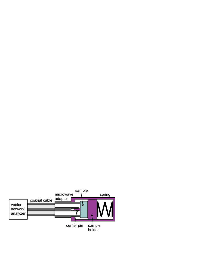
The experimental arrangement for complex permittivity measurements, where the material under investigation is placed at the aperture of a coaxial probe, allows for a broadband phase sensitive measurement of the reflection coefficient using a vector network analyzer. In case of solid matter some smart jig is needed to press the flat sample surface against the sensor Anlage ; SD , as depicted in Fig. 1. Metallic contacts (gold or aluminium) are usually evaporated on top of the solid specimen that match the inner and outer conductors of the coaxial probe in size. These contacts provide a proper electrical connection between the sample material and the probe, and they define the geometry of the sample surface exposed to the signal. The sensor can be inserted into a temperature-controlled environment and, for a given probe size, there is a useable frequency range as broad as two orders of magnitude.
The problem of extracting the interesting material parameters from the measured reflection coefficient data can be solved in two steps: first, one needs to obtain the complex sample impedance from the measured reflection coefficient ( parameter), and second, the complex material properties have to be calculated from the impedance.
II.1 Evaluation procedure for metallic samples
The evaluation of metallic samples has been developed and
experimentally tested in the recent years Anlage ; SD :
The first task is to obtain the complex sample impedance from the reflection coefficient , measured by the test set of the network analyzer, like the HP 8510. The general error model for a reflection measurement HFLange results in the following relation:
| (1) |
between the measured parameter and the actual reflection coefficient of the sample. The three independent complex values , and comprise the contribution of the microwave line. To determine those, measurements of three independent calibration samples with known actual reflection coefficients as functions of frequency and temperature are required. We use bulk aluminium samples as short, teflon samples as open and thin metallic NiCr films as load standards.
The sample impedance then follows directly via Pozar :
| (2) |
where is the characteristic impedance of the
microwave line.
The way to extract the complex electric conductivity of a metallic sample from its complex impedance is straightforward, if the thickness of the specimen either significantly exceeds the skin depth or vice versa:
-
•
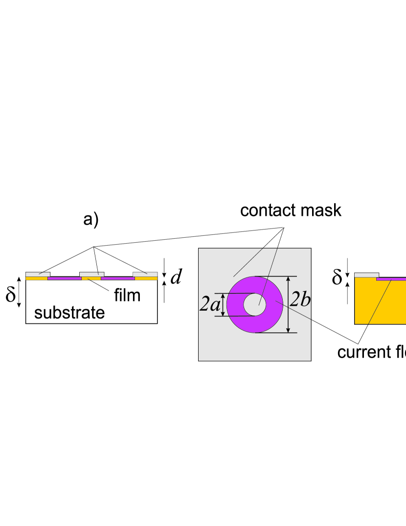
. (Fig. 2a) In case of a thin film evaporated on an insulating substrate, the electric field strength stays nearly constant throughout the whole film thickness . The relation between the conductivity and depends only on the geometry of the contacts. For the ring of inner radius and outer radius between the contacts, it reads:
(3) -
•
. (Fig. 2b) For typical microwave frequencies, the electromagnetic wave in a thick metallic sample is significantly damped already at the depth of 1 m by the skin effect. Hence, the interaction with the incident wave takes place in a thin layer at the sample surface. Boundary effects at the edges of the relatively broad contact area (cf. Fig. 2) are negligible and the concept of the surface impedance based on the assumption of plane wave propagation works well Drs . In case of a ring with inner and outer radii and , the formula to extract the conductivity from the measured impedance reads simplified :
(4) with the magnetic permeability of vacuum and the free space permittivity .
II.2 Formulation of the problem for semiconducting materials
For materials with non-metallic conductivity, none of the simple assumptions valid for metallic samples hold and both steps of the evaluation procedure contain additional challenge:
-
1.
For the calibration of the microwave line the open standard is as significant as the short and the load standards, when insulating samples are measured. It acts as a complex capacitor and the dc assumption , corresponding to , is not sufficient at higher frequencies. The correct frequency dependence of the reflection coefficient is indispensable, as shown in Sec. V.
-
2.
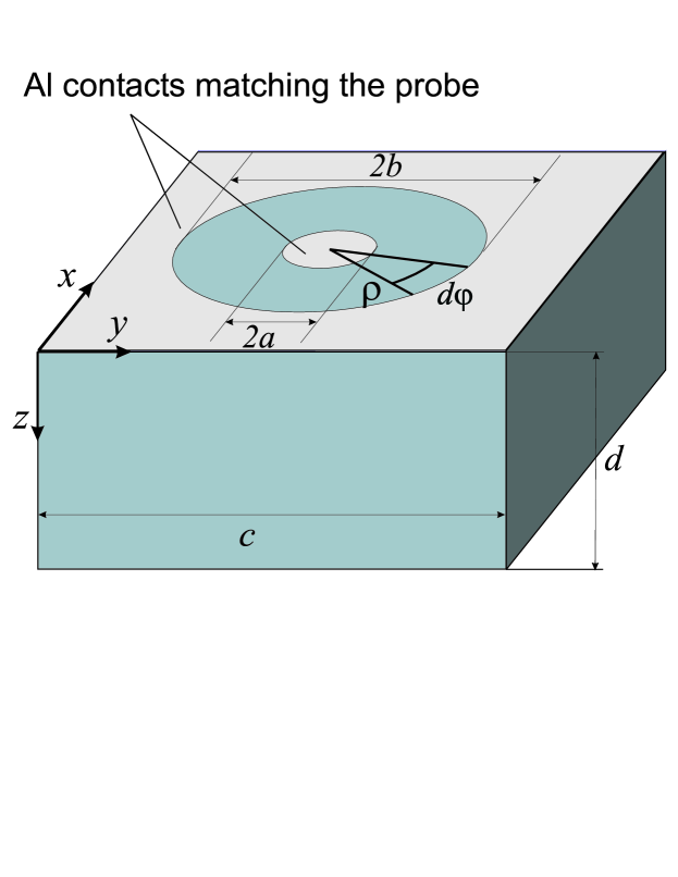
The electromagnetic wave penetrates deep into a non-metallic sample because – in contrast to a metal – the real part of the dielectric permittivity is positive. Field decay in the sample is only caused by the geometry and determined by the electric contacts (and, only to some minor degree, by the low absorption due to the imaginary part of ). In case of a 2.4 mm coaxial probe, the electric field strength falls below 1 % of its original value at the sample surface only after penetrating more than 2.5 mm, for frequencies up to 5 GHz and relative dielectric constant up to 50. With other words, the penetration depth of the electric field is of the order of the contact area dimensions (compare Fig. 3) and increases rapidly with rising frequency and permittivity. Thus, in contrast to the metals, the spatial field distribution which forms inside an insulating semiconductor is significantly different from that of a plane wave and it depends on frequency. Its knowledge is essential to extract the complex conductivity (or permittivity ) of such a sample from its complex impedance . Integral equations, implying the accurate solution for the electromagnetic field in the sample, cannot be directly solved for . Hence, approximations are required or simplified models need to be developed, with a limited range of validity for frequency and permittivity.
In the next three Sections we treat the problem of extracting the material parameters of a semiconducting sample from the impedance data. We first suggest in Sec. III a simple static model which yields already a good approximation. In Sec. IV we make use of the results by Levine and Papas LP and Misra M to relate the complex impedance of a semiconducting sample to its complex permittivity. In the following, the rigorous electromagnetic field distribution from Sec. IV is used in Sec. V to determine the frequency dependence of the reflection coefficient of the open standard for the calibration step mentioned above.
III A static model for the relation between the sample impedance and the complex conductivity
As a first approach to extract the conductivity of a low-loss semiconducting sample from its impedance, we developed a simple static model for the current distribution in a sample, based on the following assumptions:
-
1.
The response is local:
(5) where is the electric current density and is the electric field vector. This assumption implies that the electric field does not vary significantly at the distances of the mean free path , which in the case of hopping transport is the mean separation of the hopping partners.
-
2.
The dependence of the electric field on the cylindrical coordinates and can be accounted for separately. There is no dependence on the angular coordinate due to the radial symmetry of the problem.
- 3.
-
4.
As far as the dependence of the electric field strength is concerned, we assume that the field is concentrated at the surface and gets weaker for further depth because the path length for the corresponding current element d increases.
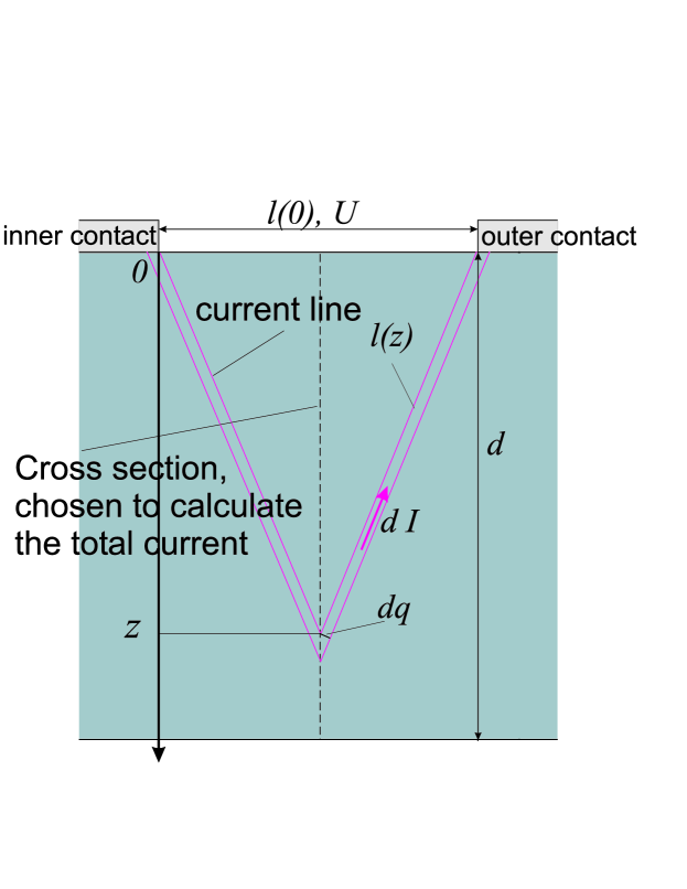
Figure 4: (color online) Geometry of the current distribution in a semiconducting sample of thickness , with metallic contacts at distance (cf. Fig. 3) as assumed in the static model. In order to calculate the total current flowing through a sample, we have chosen the cross section of the sample at the mid-distance between the Al-contacts (Fig. 4). The single current line is approximated by a triangle shape with the apex at the mid-distance cross section. Hence, we consider each infinitesimal current line at its lowest point designated by the coordinate and assume for the corresponding electric field to be reciprocally proportional to the length of the current line in order to keep the voltage constant:
(7) where .
Now that is constructed, we can calculate the total current flowing through a semiconducting sample using Eqs. (5)-(7). The integral is taken over the entire mid-distance cross section (see Fig. 4) with the infinitesimal element :
where (Fig. 4). Thus, we have obtained a relation between the complex impedance at the sample surface and the complex conductivity :
| (8) |
In the limiting case of a thin conducting film there is a simple geometrical relation between the conductivity and the impedance because the dependence of the electric field and the boundary effects can be neglected. This allows us to check the above formula in the limit , where we recover the Eq. (3).
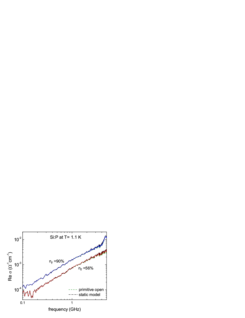
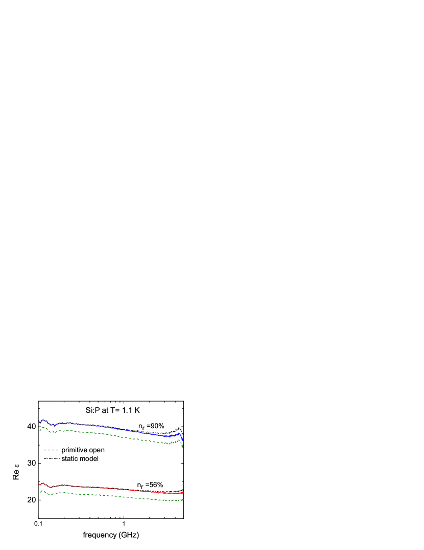
The static model has been applied to analyze frequency dependent impedance measurements of Si:P at low temperatures. As demonstrated by the dash-dotted lines in Figs. 5 and 6, the results of Eq. (8) agree very well with the rigorous solution outlined in the following Sections. Deviations can be noticed only above 1 GHz in the dielectric constant.
IV Relation between the complex impedance and the complex permittivity of a semiconducting sample
IV.1 General considerations
A large variety of methods have been developed in the past to extract the properties of low-loss and lossy dielectrics from a reflection coefficient measurement in the radio-frequency and microwave range. Simple ingenious models and analytical solutions, that are valid in a limited parameter range, have been suggested; time-consuming but arbitrarily precise numerical approaches have been treated depending on the specific practical goals. A comprehensive list of references is available in review articles like Ref. PM, .
In studies of soft and liquid materials, the coaxial probe was frequently modelled as an equivalent circuit consisting of several fringe-field capacitors in the lumped-element approach Stuchlies ; Grant ; Clark1 ; Clark2 . In Ref. Grant, a comprehensive, detailed and critical revision of this method can be found. The most striking point is the strong dependence of the model capacitances on the permittivity of the material that terminates the coaxial line, thus the approach is limited to specimens with dielectric properties close to those of the reference materials available.
Here we consider a convenient analytical way to extract the complex conductivity from the sample impedance based on the works of Levine and Papas LP and Misra M . The method is valid at least up to 5 GHz for the 2.4 mm probe and relative dielectric constants up to 50; an extension to higher frequencies is possible with certain numerical procedures added. As an intermediate result, there is an integral expression for the sample admittance as a function of the material dielectric function , which is well suited to determine the frequency dependence of the open calibration standard in a closed manner (Secs. II.2 and V). The theoretical expressions for the electromagnetic field on both sides of the sensor apertureLP are rewritten for the case of a medium with an arbitrary complex permittivity in the sample half-space. For the parameter range considered here higher_modes , we regard the variational principle applied by Levine and Papas as preferable to the precise but time-consuming numerical method of point-matching proposed by Mosig Mosig ; Grant .
IV.2 Solution in form of an integral equation
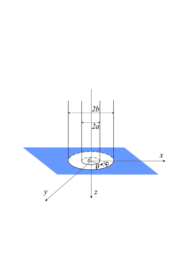
In the following, the coaxial wave guide with a center conductor of radius and an outer conductor of radius is terminated by an infinite-plane conducting flange at (Fig. 7). Choosing the dimensions and of the coaxial line to be small enough, the assumption of a single propagating mode (the principal TEM mode) in the coaxial region is justified in the covered frequency range. This system is amenable to a detailed theoretical analysis LP that yields the electromagnetic field distribution in the half-space and a relation between the aperture admittance (current-to-voltage ratio at ) and the complex wave vector of the free space .
We may assume an insulating sample to fill the half-space by choosing its finite dimensions to be large enough for the electromagnetic field strength so that the sample boundaries are negligible (cf. Sec. II.2). The results for the free space thus transform into a relation between the admittance measured at the sample surface and its complex dielectric function full_wave (here, a harmonic time dependence is assumed for the electromagnetic fieldnotation ):
| (9) |
where
| (10) | |||
| (11) |
and is the wave vector of the coaxial line with the characteristic admittance Pozar
| (12) |
The validity of the variational approximation (9) has been proven in Ref. LP, in the parameter range and by comparison with experimental results. To obtain low-temperature microwave data on Si:P with widely varying phosphorus concentration , we employ a coaxial probe of dimensions mm, mm. The maximum frequency range spans from 45 MHz to 40 GHz (limited by source and test set of the network analyzer HP 8510) and the relative dielectric constants reach from 18 till 50. This corresponds to and and lies within the tested parameter range.
IV.3 Solution of the inverse problem
The inverse problem of extracting from the measured impedance using Eq. (9) has been solved in the quasi-static approximation by Misra M . For low frequencies, the exponential function in Eq. (9) can be approximated by the first four terms of its series expansion:
| (13) |
The second term of Eq. (13) vanishes upon integration, and the last one is readily integrated; the integrals corresponding to the first and the third terms need to be numerically evaluated:
| (14) |
where
and
In our special case the relative contribution of the last term in Eq. (14) to is below 1% up to 5 GHz and the formula thus reduces to a quadratic equation for :
| (15) |
The values of the geometrical integrals for the special case of the coaxial probe with the inner and outer conductor diameters mm and mm are listed in Tab. 1.
| , mm | , mm3 | , mm4 | , mm5 |
|---|---|---|---|
| 0.9084 | -0.2100 | -0.4001 | -0.4047 |
It should be mentioned that the integrand of diverges at . That integral was numerically evaluated as the limit of a series of integrals which lower bounds converge to .
V Open calibration standard
The frequency dependence of the open calibration standard with a known dielectric function can be obtained as follows. The expression (9) of the admittance as a function of describes the open standard admittance correctly as long as the effect of the finite sample dimensions is negligible. Using a teflon block of the form shown in Fig. 3 and assuming its dielectric function to be in the GHz frequency range teflon , the maximum electric field strength at the depth of 2 mm turns out to be far below 0.01 of its value at the sample surface for frequencies up to 10 GHz, so that the secondary reflections at the back side of the open standard can be neglected here.
In order to obtain a closed expression from the integral equation (9), the series expansion of the exponential function can be used as in the previous section. In contrast to the inverse problem discussed in Sec. IV, there is no need to spare at the accuracy truncating the series early here. The relative contribution of the subsequent term being far below 10-4 up to 10 GHz, the ultimate expression we use is:
| (16) |
where
and is defined in Eq. (11). The values of the geometrical integrals for the 2.4 mm coaxial probe are listed in Table 1.
The frequency dependent reflection coefficient of the open calibration standard follows using Eq. (2):
| (17) |
The effect of the frequency dependence of on the conductivity and permittivity spectra compared to the dc assumption is demonstrated in Figs. 5 and 6 on the example of two Si:P-samples with donor concentration of 0.56 and 0.9 relative to the concentration value at the metal-insulator transition, cm-3. For samples with larger dielectric constant and higher losses , as rises, the influence of this correction slightly decreases. This is also what one would expect, when the electric properties of the material under investigation approach the metallic characteristics.
VI Application to the hopping transport in Si:P
VI.1 Dynamical conductivity
With the method described in the previous parts, Secs. IV and V, we study the frequency-dependent hopping transport in Si:P in order to explore the influence of electronic correlations Ritz . At concentrations of phosphorus in silicon below the critical value of cm-3, the donor electron states are strongly localized due to disorder in Anderson sense Anderson ; ESbook . Since some degree of compensation by impurities of the opposite type is inevitable, charge transport at low excitation energies is by variable-range hopping between the donor sites, randomly distributed in space ESbook ; Mott . Thus, theoretical models for a disordered system with electron-electron interaction are appropriate to interpret the electric conductivity spectra ES . The main issue we address is that of power laws of the frequency-dependent conductivity at zero temperature:
| (18) |
From the theory of resonant photon absorption by pairs of states, one of which is occupied by an electron and the other one is empty, distinct limiting results are known for the conductivity power law depending on which of the relevant energy scales of the problem dominates over the others:
Taking into account the Coulomb repulsion if both states in a pair would be occupied by an electron ( is the most probable hopping distance), Shklovskii and Efros derived to be a sub-linear function of frequency, as long as the Coulomb interaction term dominates over the photon energy ES . At higher frequencies, in the opposite limit, the sub-quadratic behavior known from Mott Mott for non-interacting electrons is recovered. In addition, it is known that due to electronic correlations an area of reduced density of states is formed around the Fermi level, the so-called Coulomb gap . For the conductivity of interacting electrons where the Coulomb term dominates over the photon energy but falls inside the Coulomb gap , the reduction of the density of states leads to a stronger, slightly super-linear power law ES . In order to gain some insight into the effects of electronic correlations, it is required to extract thoroughly the frequency-dependent conductivity and the related power-laws over a wide spectral range for a variety of doping concentrations.
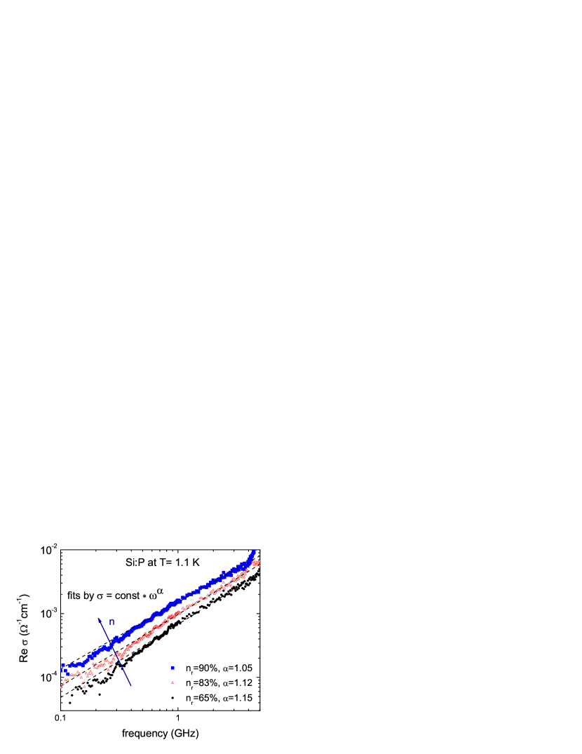
In Fig. 8 the measured real part of the frequency-dependent conductivity is plotted on a log-log scale to identify the power law. The fits by a two-parameter function are shown by the dashed lines. The frequency dependence of the conductivity clearly follows a super-linear power law in the whole doping range, where the exponent decreases with doping Ritz . From this we infer, that hopping transport takes place deep inside the Coulomb gap . A super-linear conductivity power law was previously observed in Si:As and Si:P by Castner and collaborators DC ; MC using resonator techniques at certain frequency within the range of the present work. Our results are in accord with the measurements on similar samples at higher frequencies (30 GHz to 3 THz) using optical techniques Hering1 ; Hering2 . In contrast, a sub-linear frequency dependence in the zero-phonon regime has been reported by Lee and Stutzmann Lee based on experiments on Si:B in the microwave range and by Helgren et al. Helgren using quasi-optical experiments.
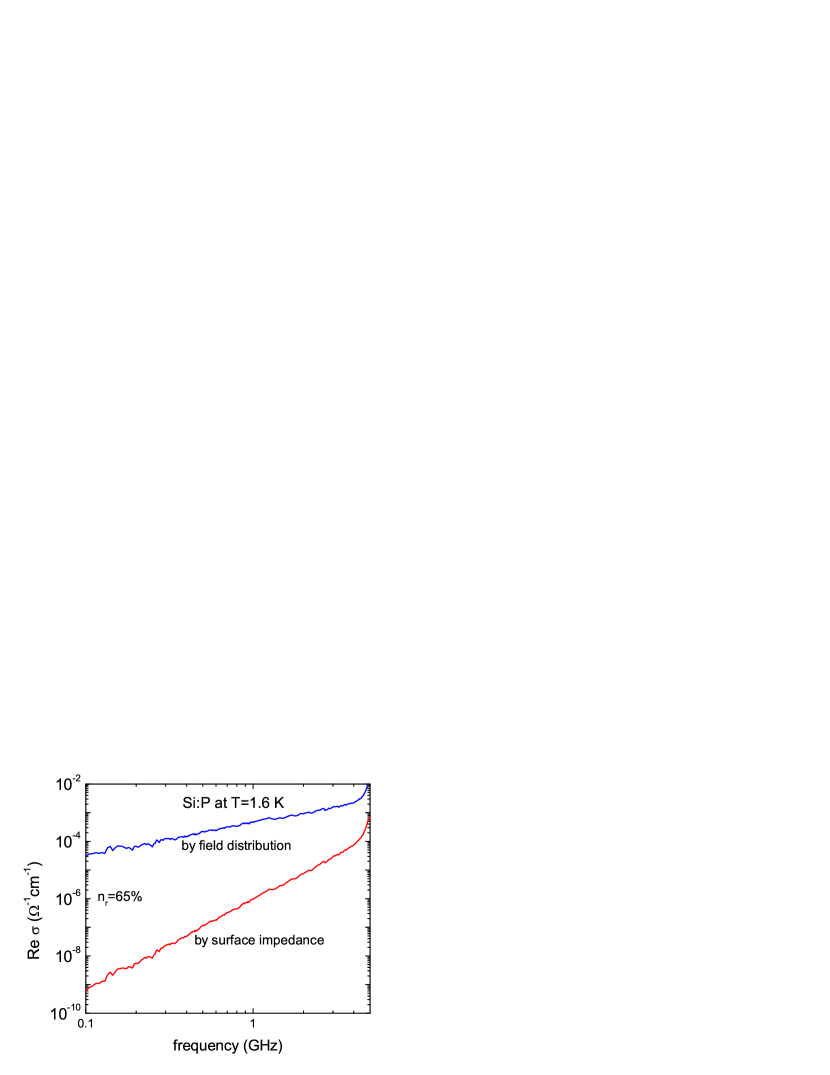
As demonstrated in Fig. 9, the surface impedance approach, mentioned in Sec. II.1, yields a wrong (i.e. too strong) frequency dependence of the conductivity for insulators. The evaluation of the impedance spectrum of a Si:P-sample is shown using the surface impedance formula (4) in comparison to the solution of the equation (15). The latter method yields a conductivity power law of approximately one, as expected from the theory outlined above.
VI.2 Dielectric function
It is an additional advantage of a phase sensitive measurement to gain the dielectric function from the imaginary part of the complex conductivity Drs :
| (19) |
We denote by the full complex dielectric function of Si:P, relative to the free space permittivity . As the metal-insulator transition is approached upon doping , the localization radius diverges ESbook . As a consequence, the electronic contribution to the dielectric function is also expected to diverge following a power law when the metal-insulator transition is approached ESepsilon :
| (20) |
where is the dielectric constant of the host material Si.
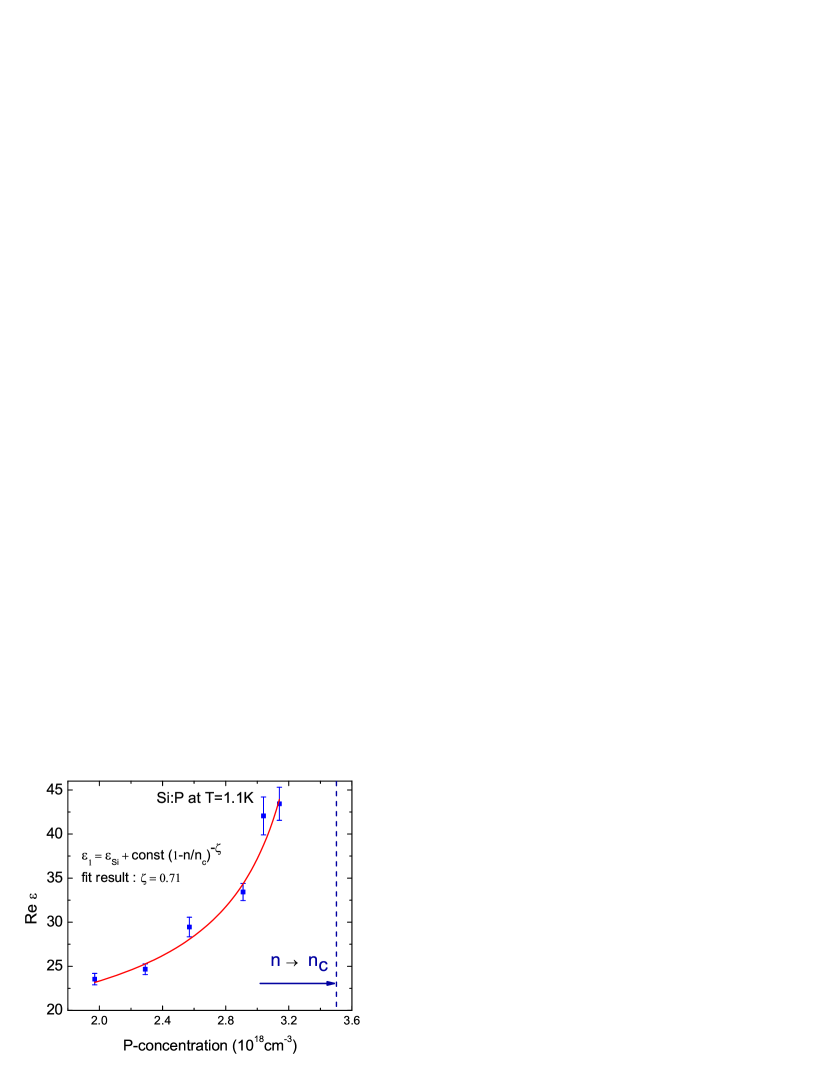
From our experiments Ritz we find that the dielectric function is independent of frequency in the range from 50 MHz to 10 GHz, taking the measurement uncertainty into account (Fig. 6). A fit with the function (20) results in an exponent 0.71, as shown in Fig. 10.
In the framework of the effective medium approximation is expected ESepsilon . From the quasi-optical experiments on Si:P different results are reported. Helgren et al. Helgren observe a similar dependence of the values of the dielectric constant on the donor concentration (though uniformly shifted to lower values by 8). Hering et al. Hering2 have observed values of as we have, but with a much stronger donor concentration dependence of the dielectric constant, resulting in a much higher exponent . It is obvious that this enormous discrepancy calls for further experiments which are more accurate as far as this analysis is concerned.
VII Conclusions
We have thoroughly analyzed the problem of extracting the electrical conductivity and permittivity from the complex impedance measured in the microwave range using a network analyzer. While for thin metallic films and bulk metals simple relations are readily available, special care has to be taken in the case of semiconductors and insulators where the electric field penetrates and decays over an appreciable distance. Already a static model with an approximate field configuration leads to reasonable results. Eventually we present a rigorous solution of the problem with basically no restricting assumptions. The advanced analysis is applied to the broadband impedance measurements of Si:P with different doping concentrations and spanning a wide range of frequency. The findings can now be compared to the theory and yield important insight into the effects of electronic correlations on the hopping transport at low temperature.
Acknowledgements
The work was partially funded by the Deutsche Forschungsgemeinschaft (DFG). ER would like to acknowledge a scholarship by the Landesgraduierten-Programm of Baden-Württemberg.
References
- (1) Compound Semiconductor Electronics, edited by S. Shur (World Scientific, Singapore, 1996); RF and Microwave Semiconductor Device Handbook, edited by M. Golio (CRC Press, Boca Rato 2003)
- (2) Electron-Electron Interactions in Disordered Systems, edited by A. L. Efros and M. Pollak (North-Holland Physics Publishing, Amsterdam, 1985)
- (3) H. v. Löhneysen, Festkörperprobleme/Adv. Solid State Phys. 30, 95 (1990); Phil. Trans. R. Soc. London A 356, 139 (1998); Festkörperprobleme/Adv. Solid State Phys. 40, 143 (2000).
- (4) M. Dressel and G. Grüner, Electrodynamics of Solids (Cambridge University Press, Cambridge, 2002)
- (5) J. C. Booth, Dong Ho Wu, and S. M. Anlage, Rev. Sci. Instrum. 65, 2082 (1994)
- (6) M. Scheffler and M. Dressel, Rev. Sci. Instrum. 76, 074702 (2005)
- (7) M. A. Stuchly and S. S. Stuchly, IEEE Trans. Instrum. Meas. IM-29, 176 (1980)
- (8) J. R. Mosig, J. C. E. Besson, M. Gex-Fabry, and F. E. Gardiol, IEEE Trans. Instr. Meas. IM-30, 46 (1981)
- (9) G. B. Gajda and S. S. Stuchly, IEEE Trans. Microwave Theory Tech. MTT-31, 380 (1983)
- (10) L. S. Anderson, G. B. Gajda and S. S. Stuchly, IEEE Trans. Instrum. Meas. IM-35, 13 (1986)
- (11) D. K. Misra, IEEE Trans. Microwave Theory Tech. MTT-35, 925 (1987)
- (12) J. P. Grant, R. N. Clarke, G. T. Symm, and N. M. Spyrou, J. Phys. E: Sci. Instrum. 22, 757 (1989)
- (13) S. Fan, K. Staebell, and D. Misra, IEEE Trans. Instr. Meas. 39, 435 (1990)
- (14) G. Q. Jiang, W. H. Wong, E. Y. Raskovich, W. G. Clark, W.A. Hines, and J. Sanny , Rev. Sci. Instrum. 64, 1614 (1993)
- (15) G. Q. Jiang, W. H. Wong, E. Y. Raskovich, W. G. Clark, W.A. Hines, and J. Sanny , Rev. Sci. Instrum. 64, 1622 (1993)
- (16) S. Evans and S. C. Michelson, Meas. Sci. Technol. 6, 1721 (1995)
- (17) C. L. Pournaropoulos and D. K. Misra, Meas. Sci. Technol. 8, 1191 (1997)
- (18) See, for example, Taschenbuch der Hochfrequenztechnik, edited by K. Lange and K.-H. Löcherer (Springer Verlag, Berlin, 1992) or Hewlett Packard Application Note 183, p. 39 (1978)
- (19) D. M. Pozar, Microwave Engineering (John Wiley & Sons, New York, 1998)
- (20) In literature (e.g. Ref. Anlage, ) a simplified formula can be found, that follows from the equation (4) if is neglected and the sign of the imaginary part of is defined in a different way according to the complementary sign notation in the exponent of the Fourier-transformed of the electromagnetic fields (cf. Ref. notation, ).
- (21) H. Levine and C. H. Papas, J. Appl. Phys. 22, 29 (1951)
- (22) The variational approximation applied by Levine and Papas LP leads to a vanishing contribution of the integral terms corresponding to the evanescent higher order terms of the electromagnetic wave inside the coaxial sensor. The parameter range, where the corresponding uncertainty in the resulting capacitances is below 1%, as proved by Levine and Papas, includes our range of frequency and dielectric function. Moreover, Misra M has critically compared the method with the results obtained by Mosig Mosig under consideration of higher order modes, yielding a parameter range where the variational approximation is justified.
- (23) For effectively smaller samples, a full wave treatment considered by Brom and collaborators B is necessary, which takes secondary reflections at the sample back into account.
- (24) H. C. F. Martens, J. A. Reedijk, and H. B. Brom, Rev. Sci. Instrum. 71, 473 (2000)
- (25) We hold to the convention for the Fourier-transformed of the electromagnetic field in accordance with Refs. Drs, ; LP, . The opposite sign convention is used in Refs. B, ; M, and by the network analyzer.
- (26) Micro-Coax data on the solid PTFE as a dielectric of the semi-rigid cable UT 085B-SS, at frequency of 1 GHz, =2.03(1+i0.0002).
- (27) E. Ritz and M. Dressel, arXiv:0711.1256, in print phys. stat. sol. (c)
- (28) P. W. Anderson, Phys. Rev. 109, 1492 (1958)
- (29) B. I. Shklovskii and A. L. Efros, Electronic Properties of Doped Semiconductors (Springer, Berlin, 1984),
- (30) N. F. Mott and E. A. Davis, Electronic Processes in Non-Crystalline Materials, 2nd edition (Clarendon Press, Oxford, 1979),
- (31) B. I. Shklovskii and A. L. Efros, Zh. Eksp. Teor. Fiz. 81, 406 (1981) [Sov. Phys. JETP 54, 218 (1981)]
- (32) R. J. Deri and T. G. Castner, Phys. Rev. Lett. 57, 134 (1986)
- (33) M. Migliuolo and T. G. Castner, Phys. Rev. B 38, 11593 (1988)
- (34) M. Hering, M. Scheffler, M. Dressel, and H. v. Löhneysen, Physica B 359, 1469 (2005)
- (35) M. Hering, M. Scheffler, M. Dressel and H. v. Löhneysen, Phys. Rev. B 75, 205203 (2007)
- (36) M. Lee and M. L. Stutzmann, Phys. Rev. Lett. 87, 056402 (2001)
- (37) E. Helgren, N. P. Armitage, and G. Grüner, Phys. Rev. B 69, 014201 (2004)
- (38) A. L. Efros and B. I. Shklovskii, phys. stat. sol. (b) 76, 475 (1976)