Finite size effects on spin-torque driven ferromagnetic resonance in spin-valves with a Co/Ni synthetic free layer
Abstract
Spin-torque driven ferromagnetic resonance (ST-FMR) is used to study magnetic excitations in Co/Ni synthetic layers confined in nanojunctions. Field swept ST-FMR measurements were conducted with a magnetic field applied perpendicular to the layer surface. The resonance lines were measured under low amplitude excitation in a linear response regime. The resulting resonance fields were compared with those obtained using conventional rf field driven FMR on extended films with the same Co/Ni layer structure. A lower resonance field is found in confined structures. The effect of both dipolar fields acting on the Co/Ni layer emanating from other magnetic layers in the device and finite size effects on the spin wave spectrum are discussed.
One approach to study ferromagnetic resonance (FMR) of a magnetic layer in a confined structure is to use the spin transfer interaction Slonczewski (1996); Berger (1996) in a current-perpendicular (CPP) nanojunction. An rf current is applied to a magnetic tunnel junction Tulapurkar et al. (2005) or spin valve Sankey et al. (2006), to drive FMR, in a method known as the spin-torque-driven ferromagnetic resonance (ST-FMR). This new technique enables quantitative studies of magnetic properties of materials in nanopillars, such as their magnetic excitations, anisotropy and damping.
Spin-transfer devices that incorporate materials with perpendicular magnetic anisotropy are of great interest. This is because of their potential to lead to faster ST-devices, with lower power dissipation Kent et al. (2004) and critical current Sun (2000). Recently, Mangin et al. studied perpendicular spin valves with a Co/Ni multilayer free layer, where a large magnetoresistance value and a high spin torque efficiency were observed Mangin et al. (2006).
In this work, we present ST-FMR studies on bilayer spin valves, where the thin (free) layer is composed of a Co/Ni synthetic layer and the thick (fixed) layer is pure Co. By comparing the ST-FMR resonance fields with those of conventional rf field driven FMR of extended Co/Ni films with the same layer structure, we illustrate interactions important in ST-FMR of nanojunctions. Specifically, we discuss both dipolar interactions between the Co/Ni layer and other magnetic layers in the device, and finite size effects on the magnetic excitation spectrum.
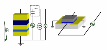
Pillar junctions with submicron lateral dimensions and rectangular shape, shown in Fig. 1a, were patterned on a silicon wafer using a nanostencil process Sun (2002). Junctions were deposited by evaporation, and have the layer structure nm Cr nm Cu nm Pt nm Cu [0.4 nm Co 0.8 nm Ni] nm Cu nm Co nm Cu. The ST-FMR measurement setup is shown in Fig. 1(a). An rf current generated by a high frequency source is coupled with a dc current through a bias-T (the dashed-line box in Fig. 1(a)) into the spin valve. At resonance, the rf current and spin valve resistance oscillate at the same frequency. This results in a dc voltage () Tulapurkar et al. (2005); Sankey et al. (2006). Assuming a small angle circular precession of the free layer on resonance,
| (1) |
where is the angle between the free and fixed layers (before applying the rf current) and is the precession angle. represents the rf current amplitude in the junction, and () is the static junction resistance when free layer and fixed layer are antiparallel (parallel) to each other. With a perpendicular magnetic field greater than the free layer’s easy-plane anisotropy field, the free layer magnetization is normal to the surface, while the fixed layer, which has a larger easy-plane anisotropy field, is still mainly magnetized in the film plane. In this way, the signal is maximized, according to Eq. 1. To improve the signal (typically in the sub-V range) to noise ratio, we modulate the rf current on and off at 800 Hz and use a lock-in amplifier to detect the voltage at this frequency.
Extended films with the same stack as the free layer were deposited on an oxidized Si wafer using the same deposition technique. It has the same Co/Ni synthetic layer sandwiched between 10 nm of Cu on each side. As is shown in Fig. 1(b), it was measured by placing the film onto a 50-Ohm-matched coplanar waveguide Beaujour et al. (2006). An rf current was sent through the waveguide and generates an rf field that drives the magnetic film into resonance. The transmission of the rf signal was measured using a network analyzer, as a function of rf frequency and external magnetic field.
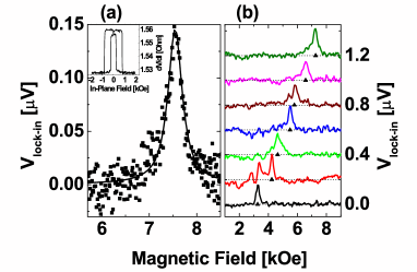
The magnetoresistance (MR) of the nanojunctions was measured using a four-point geometry with the magnetic field applied in the film plane. A typical MR hysteresis loop of a 50150 nm2 junction is shown in the inset of Fig. 2(a). MR, is for a total of 10 junctions studied.
ST-FMR measurements were conducted with the external magnetic field applied nearly perpendicular to the film plane ( off the normal direction as shown in Fig. 1(a), where the small in-plane component is along the easy-axis of the junction, in order to avoid vortex states in the free layer). This was measured using a two-point geometry. Fig. 2(a) shows a typical field-swept resonance line at a fixed rf frequency of 18 GHz and zero dc current. It was measured on the same junction on which the data in the inset was taken. The resonance is fit by a Lorentzian, indicated by the solid line. From the peak height , we estimate the precession angle to be using Eq. 1. We verified that this data was taken in a linear response regime with independent of .
A series of ST-FMR resonance lines at different rf frequencies were measured within the low amplitude linear regime. Those with 7 different rf frequencies (416 GHz in 2 GHz steps) are plotted in Fig. 2(b), with each adjacent curve offset by V. The resonance field ( in Fig. 2(b)) increases linearly with greater than 4 GHz. At 4 GHz, the perpendicular magnetic field at resonance is lower than the easy-plane anisotropy field of the free layer. Therefore, the free layer magnetization tends to tilt into the plane, leading to a lower resonance field. Similar dispersion relationships have been found on junctions with other lateral dimensions.
The resonance field for both extended films and nanojunctions as the function of are plotted in Fig. 3(a). Black dots are for a similar spin valve with the same lateral dimension and pink dots for the same-stack extended film. Further details on the conventional FMR experiments can be found in Ref. Beaujour et al. (2007). Red and blue solid lines are their corresponding linear fits above 4 GHz. By comparing these two sets of data, we find a slight difference in slope and a small shift in the zero frequency intercept. The relationship between and in the extended film is given as: Kittel (1996) in the case where the magnetization is normal to the film surface. Here g is the Landé g factor of the film, and the easy-plane anisotropy is , where and represent the saturation magnetization, and the perpendicular anisotropy field. A direct linear fit of each data set gives a slope g=2.17, field-axis intercept kOe for the extended film, and a slightly larger slope (2.28) and a smaller field-axis intercept (1.92 kOe) for the confined structure in the spin valves. Such a consistency confirms that the main peak of the ST-FMR signal comes from the Co/Ni synthetic free layer rather than the fixed Co layer Footnote1 .
We now estimate the effect of dipolar fields from other magnetic layers in spin valves, which come from the fixed Co layer and the junction level magnetic residuals outside the stencil holes Sun (2002). from the normal component of the fixed Co layer is not negligible. At GHz, the Co layer is tilted out-of-plane at , and the component of normal to the film surface is 500 Oe. At higher frequencies, the normal component of is larger since the fixed Co layer magnetization is more tilted out-of-plane for larger . of the junction level Co residual is estimated to be 15 times smaller, while that of the junction level Co/Ni residual has a constant -120 Oe field contribution normal to the surface. The in-plane component of the dipolar fields ( 260 Oe) shifts down by 30 Oe at 4 GHz, and this shift is significantly reduced at higher frequencies. Therefore, the dipolar fields from the normal component of the fixed Co layer and from the junction level Co/Ni residual are important in biasing of free layer in spin valves. The dashed line in Fig. 3(a) is the linear fit of with the dipolar field correction. In the new linear fit, the slope becomes 2.18, which is almost the same as the g factor of the extended film, and the field-axis intercept becomes 2.13 kOe. A 450 Oe shift between them at all frequencies still remains.
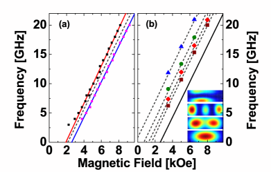
Similar results have been found in other spin valve junctions. ST-FMR results taking into account the dipolar fields from other magnetic layers in the device show a similar g-factor (2.180.03) with a 370570 Oe lower resonance field than that of the extended film. Numerical calculation on the normal spin wave (SW) modes in elliptical Py disks was presented in Ref. McMichael and Stiles (2005), and the resonance shift of different SW modes due to the finite size effect was discussed. In order to estimate the resonance shift in our rectangular Co/Ni synthetic nanoelement, we have also done micromagnetic simulations using OOMMF Donahue and Porter (1999), which includes the Zeeman, exchange and magnetostatic contributions to the energy (but not the spin transfer interaction). The modes of a 50150 nm2 element are shown in lower-right of Fig. 3(b). The mode resonance is shifted towards lower field as the order of the SW modes becomes higher (dots in Fig. 3(b)). The lowest order SW mode is shifted by 1 kOe from the thin film result (solid line). This shift is the same order of magnitude as found in our experiments. It is larger than that observed possibly because the lateral dimensions of the pillar are larger than the nominal dimensions. The 2nd mode is close to the lowest one, while 3rd and 4th ones are further apart. This shows the effect of finite size and mode structure on the resonance field. Furthermore, multiple peaks found at several frequencies (see Fig. 2(b) at GHz, for example), may be due to the excitation of higher order SW modes.
An analytical estimation of the energy of the SW modes in a rectangular element enables a better understanding of the physics. The idea is to assume a sinusoidal profile of the eigenmode in the finite rectangular element Bailleul et al. (2006), and to use the dipole-exchange dispersion of the SW modes in a perpendicularly magnetized film Kalinikos and Slavin (1986):
| (2) |
where is the gyromagnetic ratio, and the internal field , where is the demagnetization factor in the normal direction. is the exchange term, with A and k representing exchange constant and in-plane wave vector. is the dipolar term in which t is the thickness of the disk, and it describes the SW dynamic dipole-dipole interaction. Moreover, as discussed in Ref. Guslienko et al. (2002), the oscillating magnetization is only partially pinned at the boundary. Thus, a larger effective lateral dimension needs to be introduced in the analytical calculation to mimic the partial pinning. The 1 kOe shift, like that in the OOMMF simulation, can be found using Eq. 2 by introducing an effective lateral dimension 70170 nm2. Using these dimensions, the higher order modes denoted as (,) are also quantitatively reproduced with , (see dashed lines in Fig. 3(b)).
In summary, we used the ST-FMR technique to measure the resonance fields of Co/Ni synthetic layers in a confined spin valve structure and compared it to that of the same-stack extended film. The effects of dipolar fields and finite element size produce changes in the resonance field that are the same order of magnitude as those observed in the experiment.
This research is supported by NSF-DMR-0706322, ARO-W911NF-07-1-0643 and an NYU-Research Challenge Fund award.
References
- Slonczewski (1996) J. C. Slonczewski, J. Magn. Magn. Mater. 159, L1 (1996).
- Berger (1996) L. Berger, Phys. Rev. B 54, 9353 (1996).
- Tulapurkar et al. (2005) A. A. Tulapurkar, Y. Suzuki, A. Fukushima, H. Kubota, H. Maehara, K. Tsunekawa, D. D. Djayaprawira, N. Watanabe, and S. Yuasa, Nature 438, 339 (2005).
- Sankey et al. (2006) J. C. Sankey, P. M. Braganca, A. G. F. Garcia, I. N. Krivorotov, R. A. Buhrman, and D. C. Ralph, Phys. Rev. Lett. 96, 227601 (2006).
- Kent et al. (2004) A. D. Kent, B. Özyilmaz, and E. del Barco, Appl. Phys. Lett. 84, 3897 (2004).
- Sun (2000) J. Z. Sun, Phys. Rev. B 62, 570 (2000).
- Mangin et al. (2006) S. Mangin, D. Ravelosona, J. A. Katine, M. J. Carey, B. D. Terris, and E. E. Fullerton, Nature Materials 5, 210 (2006).
- Sun (2002) J. Z. Sun, Appl. Phys. Lett. 81, 2202 (2002).
- Beaujour et al. (2006) J.-M. L. Beaujour, J. H. Lee, A. D. Kent, K. Krycka, and C.-C. Kao, Phys. Rev. B 74, 214405 (2006).
- Beaujour et al. (2007) J.-M. Beaujour, W. Chen, K. Krycka, C.-C. Kao, J. Z. Sun, and A. D. Kent, Eur. Phys. J. B 59, 475 (2007).
- Kittel (1996) C. Kittel, Introduction to Solid State Physics (John Wiley & Sons, Inc., 1996).
- (12) FMR measurement on 10 nm thick extended pure Co layers shows that the resonance field is much larger (a few Tesla) for 3 GHz, because of its high easy-plane anisotropy (17 kOe). At lower frequencies, the resonance field decreases rapidly as the layer magnetization tilts into the plane, with a slope far from the g seen in the ST-FMR studies.
- McMichael and Stiles (2005) R. D. McMichael and M. D. Stiles, J. Appl. Phys. 97, 10J901 (2005).
- Donahue and Porter (1999) M. J. Donahue and D. G. Porter, OOMMF User’s Guide (National Institute of Standards and Technology, 1999).
- Bailleul et al. (2006) M. Bailleul, R. Höllinger, and C. Fermon, Phys. Rev. B 73, 104424 (2006).
- Kalinikos and Slavin (1986) B. A. Kalinikos and A. N. Slavin, J. Phys. C 19, 7013 (1986).
- Guslienko et al. (2002) K. Y. Guslienko, S. O. Demokritov, B. Hillebrands, and A. N. Slavin, Phys. Rev. B 66, 132402 (2002).