Measurement of Ultrafast Carrier Dynamics in Epitaxial Graphene
Abstract
Using ultrafast optical pump-probe spectroscopy, we have measured carrier relaxation times in epitaxial graphene layers grown on SiC wafers. We find two distinct time scales associated with the relaxation of nonequilibrium photogenerated carriers. An initial fast relaxation transient in the 70-120 fs range is followed by a slower relaxation process in the 0.4-1.7 ps range. The slower relaxation time is found to be inversely proportional to the degree of crystalline disorder in the graphene layers as measured by Raman spectroscopy. We relate the measured fast and slow time constants to carrier-carrier and carrier-phonon intraband and interband scattering processes in graphene.
Graphene is a single two dimensional (2D) atomic layer of carbon atoms forming a dense honeycomb crystal lattice dressel ; nov0 . It is a zero-bandgap semiconductor with a linear energy dispersion relation for both electrons and holes nov0 . The unusual electronic and optical properties of graphene have generated interest in both experimental and theoretical arenas nov0 ; nov1 ; NovoselovGeimFirst ; zhang ; heer . The high mobility of electrons in graphene has prompted a large number of investigations into graphene based high speed electronic devices, such as field-effect transistors, pn-junction diodes and transistors, and terahertz oscillators, and also into low noise electronic sensors NovoselovGeimFirst ; lundstrom ; marcus ; gong ; rana ; chemicalsensor .
The simplest way of obtaining graphene layers is via micromechanical cleaving (exfoliation) of bulk graphite followed by careful selection of monolayers by using optical, atomic force, or scanning electron microscopes nov1 . Although this technique results in relatively high quality films, it might not be suitable for large scale production. Recently, epitaxial growth of graphene by thermal decomposition of SiC surface at high temperatures has been investigated as a promising alternative for large scale production heer ; grapheneonSiC1 . This technique can provide anywhere from a few monolayers of graphene to several () layers on the surface of a SiC wafer. Graphene layers grown by this technique have demonstrated structural and electronic properties similar to those of graphene layers obtained by micromechanical cleaving techniques, including the massless Dirac-like energy dispersion relation for electrons and holes and carrier mobilities in the few tens of thousand cm2/V-s range heer ; grapheneonSiC3 ; STMgrapheneonSiC . In addition, the electronic as well phononic properties of epitaxially grown graphene multilayers have been found to be different from those of bulk graphite and similar to those of a graphene monolayer indicating that the electrons and phonons in different layers in epitaxially grown graphene are uncoupled raman ; stacking . This observed difference in the properties of epitaxial graphene and bulk graphite has been attributed to a different stacking scheme for carbon atom layers in epitaxial graphene compared to bulk graphite stacking . Epitaxial growth of graphene on SiC provides a technique to obtain large area multilayers that can be used for studies, such as ultrafast optical spectroscopy, that are difficult to conduct on monolayers.
In this paper, we present results from measurements of the ultrafast dynamics of photoexcited carriers in graphene for the first time. Ultrafast studies of carrier dynamics in other forms of carbon, such as carbon nanotubes and bulk graphite, have been reported in the past pumpprobeCNT1 ; pumpprobeCNT2 ; pumpprobegraphite1990 . The results presented in this paper are relevant for understanding carrier intraband and interband scattering mechanisms, and the corresponding rates, in graphene and their impact on proposed and demonstrated graphene based electronic and optical devices NovoselovGeimFirst ; lundstrom ; marcus ; gong ; rana .
The graphene samples used in this work were all epitaxially grown on the carbon face of semi-insulating 6H-SiC wafers using the techniques that have been reported in detail previously grapheneonSiC1 . Samples A, B and C were grown at temperatures varying from to and pressures of torr. Micro-Raman spectroscopy of all samples showed a single-resonant G peak close to 1580 cm-1, a double-resonant D’ peak close to 2700 cm-1, and also a relatively low intensity double-resonant D peak near 1350 cm-1 raman1 ; raman . The D peak is not allowed in perfect graphene layers since it requires an elastic scattering process, which is made possible by disorder, to satisfy momentum conservation raman . The presence of the D peak therefore indicates the presence of disorder in the samples. A discussion of the observed intensity of the D peak and its correlation with the measured carrier relaxation times is presented later in this paper. Fourier Transform Infrared (FTIR) spectroscopy of the samples revealed a flat absorption profile in the entire 2.5-25 m range, which is consistent with the massless Dirac-like energy dispersion of electrons and holes (see Eqs. 1 and 2 below). The number of graphene layers in samples A, B, and C were estimated from FTIR and XPS spectroscopies (using the Thickogram method thickogram ) to be 6, 12 and 37, respectively, with less than 5 error.
A Ti:sapphire mode-locked laser with 86 MHz pulse repetition rate, 780 nm center wavelength, and 85 fs pulse width was used for time-resolved pump-probe spectroscopy of the graphene samples. Pump pulses with energies between 3-15 nJ were used to generate photoexcited carriers, while weak probe pulses with energies between 30-100 pJ were used to measure the changes in the transmittivity of the samples at various delays of the probe pulses with respect to the pump pulses. The angle of incidence of the pump and probe beams were and respectively. The pump and the probe were focused to a spot size of about 100 m. The polarization of the probe was rotated by 90 degrees with respect to the pump and a polarizer was used to eliminate scattered pump light going in the direction of the probe beam. The probe beam was passed through a 50 m spatial filter for further removal of the scattered pump light. The pump and probe beams were both modulated at two different frequencies near 3 KHz, and changes in the intensity of the probe pulses at the sum of these two frequencies were measured with a lockin amplifier.
Photon interband absorption in graphene at optical and near-infrared frequencies is given by the optical conductivity rana ,
| (1) |
where, and are the probabilities for the occupation of an energy level with energy in the conduction and valence bands, respectively. The only frequency dependence of comes from the carrier distribution functions. Matching the optical boundary conditions at the air/graphene/SiC interfaces, the optical transmission through graphene layers on a SiC wafer (normalized to the transmission through a plain SiC wafer) can be written as,
| (2) |
where, is the refractive index of SiC. The above expression can be used to estimate that pump pulses with energies in the range indicated above generate electron and hole densities in the - cm-2 range. The photogenerated carrier densities are larger than the intrinsic electron and hole densities of cm-2 in graphene at room temperature.
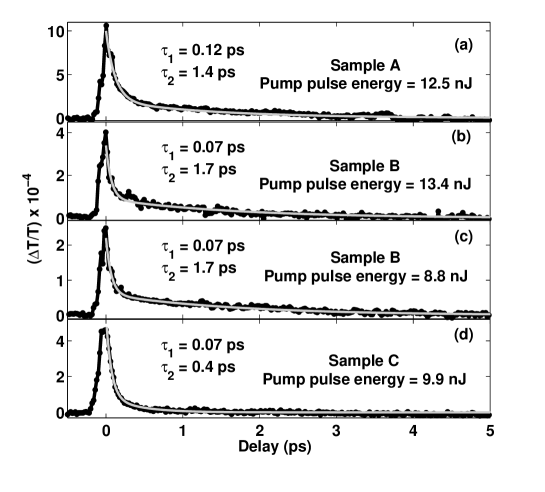
Figure 1 shows the measured transmittivity transients for different graphene samples. The figure shows the time dependent change in the transmittivity normalized to the transmittivity in the absence of the pump pulse. Transmittivity increases sharply just after photoexcitation. The recovery of the transmittivity exhibits two distinct time scales; an initial fast relaxation time in the 70-120 fs range followed by a slower relaxation time in the 0.4-1.7 ps range. These time constants have been extracted by analytical fits to the data using decaying exponentials. It should be noted here that the faster time is of the order of the pulse width and is therefore not accurately resolvable.
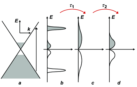
A simple model incorporating band-filling effects together with intraband carrier-carrier and carrier-phonon scattering can be used to explain the observed transmittivity transients. Figure 2 is a schematic representation of this model. As shown in Eq. 1, optical interband absorption in graphene is proportional to the difference between the occupancies of the conduction and valence bands at energies equal to (measured from the Dirac point). Photogeneration of carriers by the pump pulse reduces this difference and causes the initial increase in the transmittivity observed in Figure 1. Immediately after photoexcitation, the non-equilibrium carrier distribution broadens and also equilibrates with the intrinsic carrier population through carrier-carrier scattering. This process results in the initial fast relaxation of the transmittivity. The observed fast relaxation times () are consistent with the theoretically predicted carrier-carrier intraband scattering rates in graphene by S. Das Sarma et. al. darma . As a result of carrier-carrier scattering the photogenerated carriers are expected to equilibrate among themselves and reach a Fermi-Dirac-like distribution with a temperature much higher than the lattice temperature. The observed slower time constant () of the transmittivity decay could be attributed to the subsequent thermalization of the carriers with the lattice through carrier-phonon intraband scattering.
Electron-hole recombination processes could also contribute to the slow decay of the transmittivity. The dominant mechanisms for electron-hole recombination in graphene are not yet well understood. Electron-hole recombination due to Auger scattering in graphene was analyzed and carrier density dependent lifetimes of the order of a few picoseconds for electron-hole densities in the 1011-1012 cm-2 range were predicted by F. Rana rana2 . However, in our experiments varying the pump pulse energies in the 3 nJ to 15 nJ range to vary the photogenerated carrier densities did not lead to any significant changes in the measured values of . For example, Figures 1(b) and 1(c) show the measured transmittivity transients for two different pump pulse energies for sample B. These results indicate that the dominant contribution to comes from a process that is independent of the carrier density and is likely carrier-phonon rather than carrier-carrier scattering. However, electron-hole recombination due to carrier-phonon interband scattering cannot be ruled out. It needs to be pointed out here that carrier-phonon scattering cannot also be ruled out as a contributor to the fast relaxation time from our measurement results. Pump pulse energy dependence, and therefore carrier density dependence, of the time could not be reliably extracted from the measurements since, as already mentioned above, the observed values of were close to the pulse width used in the experiments.
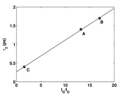
It has been shown that carrier-phonon deformation potential scattering rates in semiconductor nanostructures are enhanced in the presence of disorder disphonon . In graphene, the intensity of the double-resonant D peak (near 1350 cm-1) in the raman spectrum can be used as a measure of crystalline disorder since this peak is absent in perfect graphene layers raman ; ramandis . The ratio of the intensities, and , of the G and D peaks, respectively, in the raman spectrum has been shown to be proportional to the crystal coherence length ramandis . Thus, one could expect the measured time constant to scale with the ratio . Figure 3 shows the measured values of plotted vs the measured values of the ratio for the three samples. Figure 3 shows that and therefore is proportional to the coherence length of the crystal. These results also support electron-phonon scattering as being the dominant mechanism contributing to .
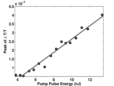
Figure 4 shows the peak value (normalized) of the measured transmittivity change plotted as a function of the pump pulse energy for sample B. As expected from linear absorption and final state filling arguments, the maximum value of is proportional to the pump pulse energy. This data also rules out any significant role played by nonlinear two-photon absorption in the transmittivity transients. Complete saturation or bleaching of the absorption is not observed for the range of pump pulse energies used in the experiments. From the density of states of graphene it follows that the maximum electron density in an energy interval centered at is , where is the velocity of carriers in graphene and equals cm/s nov0 . Putting and , where is the optical bandwidth of the pump pulse (10 nm), the maximum electron (or hole) density comes out to be cm-2 for 780 nm pump center wavelength. The fact that no bleaching of the absorption is observed even for pulse energies large enough to excite electron (and hole) densities close to cm-2 is because of the fast relaxation time that is of the order of the pump pulse width. Graphene therefore has potential for use as a fast saturable absorber for generating high energy short pulses from modelocked lasers kartner .
In conclusion, we have measured ultrafast carrier relaxation rates in epitaxially grown graphene layers on SiC. We observe two distinct time scales associated with the relaxation dynamics of photogenerated carriers. The observed time scales are comparable to those observed in other related forms of carbons, such as highly ordered pyrolytic graphite (HOPG) and single-walled carbon nanotubes pumpprobeCNT1 ; pumpprobeCNT2 ; pumpprobegraphite1990 . Our measurements indicate the separate roles played by carrier-carrier and carrier-phonon scattering in relaxing photogenerated carriers.
More work is needed to investigate the role of carrier-phonon scattering in the fast relaxation time , the role of electron-hole recombination in the slow relaxation time , and the value of in the limit of disorder-free epitaxial graphene layers. It has been recently pointed out that the first few carbon layers in epitaxially grown graphene acquire a bandgap as a result of interaction with the atoms in the SiC substrate that breaks the symmetry between the and atoms in the graphene lattice heer2 . The effect of bandgap on ultrafast intraband and interband carrier dynamics is not clear. Also, in multilayer graphene structures the optical response is likely to be dominated by the large number of layers that are not close to the substrate and do not have a bandgap. Pump-probe experiments with fewer monolayers of epitaxial graphene would be needed to explore the effects of bandgap on carrier dynamics.
The authors would like to acknowledge support from the National Science Foundation. This work was also partially supported by the Air Force office of Scientific research contract No. FA9550-07-1-0332 (contract monitor Dr. Donald Silversmith), and Cornell Material Science and Engineering Center (CCMR) program of the National Science Foundation (cooperative agreement 0520404).
References
- (1) R. Saito, G. Dresselhaus, M. S. Dresselhaus, Physical Properties of Carbon Nanotubes, Imperial College Press, London, UK (1999).
- (2) A. H. Castro Neto, F. Guinea, N. M. R. Peres, K. S. Novoselov, A. K. Geim, Submitted to Rev. Mod. Phys. (2007). Also available at cond-mat/0709.1163 (2007).
- (3) K. S. Novoselov, A. K. Geim, S. V. Morozov, D. Jiang, M. I. Katsnelson, I. V. Grigorieva, S. V. Dubonos, A. A. Firsov, Nature, 438, 197 (2005).
- (4) K.S. Novoselov, A.K. Geim, S.V. Morozov, D. Jiang, Y. Zhang, S. V. Dubonos, I.V. Grigorieva, A.A. Firsov, Science, 306, 666 - 669 (2004).
- (5) Y. Zhang, Y. Tan, H. L. Stormer, P. Kim, Y. Zhang et. al., Nature, 438, 201 (2005).
- (6) C. Berger, Z. Song, X. Li, X. Wu, N. Brown, C. Naud, D. Mayou, T. Li, J. Hass, A. N. Marchenkov, E. H. Conrad, P. N. First, W. A. de Heer, Science, 312, 1191 (2006).
- (7) G. Liang, N. Neophytou, D. E. Nikonov, M. S. Lundstrom, IEEE Trans. Elec. Dev., 54, 657 (2007).
- (8) J. R. Williams, L. DiCarlo, C. M. Marcus, Science, 317, 638 (2007).
- (9) G. Gu, S. Nie, R. M. Feenstra, R. P. Devaty, W. J. Choyke, W. K. Chan, M. G. Kane, Appl. Phys. Lett., 90, 253507 (2007).
- (10) F. Rana, To appear in IEEE Trans. Nanotechnology (2007). Also available at cond-mat/0710.3556 (2007).
- (11) F. Schedin, A.K. Geim, S.V. Morozov, E.W. Hill, P. Blake, M.I. Katsnelson, K.S. Novoselov , Nature Materials 6, 652 (2007).
- (12) C. Berger, Z. Song, T. Li, X. Li, A. Y. Ogbazghi, R. Feng, Z. Dai, A.N. Marchenkov, E.H. Conrad, P.N. First, W.A. de Heer , J. Phys. Chem. B 108, 19912 (2004).
- (13) T. Ohta, A. Bostwick, T. Seyller, K. Horn, E. Rotenberg, Sicence, 313, 951 (2006)
- (14) V.W. Brar, Y. Zhang, Y. Yayon, T. Ohta, J. L. McChesney, A. Bostwick, E. Rotenberg, K. Horn, M.F. Crommie, Appl. Phys. Lett. 91, 122102 (2007)
- (15) A. C. Ferrari, J. C. Meyer, V. Scardaci, C. Casiraghi, M. Lazzeri, F. Mauri, S. Piscanec, D. Jiang, K. S. Novoselov, S. Roth, A. K. Geim, Phys. Rev. Letts., 97, 187401 (2006).
- (16) C. Faugeras, A. Nerriere, M. Potemski, A. Mahmood, E. Dujardin, C. Berger, W. A. de Heer, cond-mat/0709.2538 (2007).
- (17) J. Hass, F. Varchon, J. E. Millan-Otoya, M. Sprinkle, W. A. de Heer, C. Berger, P. N. First, L. Magaud, E. H. Conrad, cond-mat/0706.2134 (2007).
- (18) J-S. Lauret, C. Voisin, G. Cassabois, C. Delalande, Ph. Roussignol, O. Jost, L. Capes, Phys. Rev. Lett. 90, 057404 (2003).
- (19) Y. Ma, J. Stenger, J. Zimmermann, S. M. Bachilo,R. E. Smalley, R. B. Weisman, G. R. Fleming, J. Chem. Phys. 120, 3368 (2004).
- (20) K. Seibert, G.C. Cho, W. K tt, H. Kurz, D.H. Reitze, J.I. Dadap, H. Ahn, M.C. Downer, A.M. Malvezzi, Phys. Rev. B. 42, 2842 (1990).
- (21) P. J Cumpson, Surface and Interface Analysis, 29, 403 (2000).
- (22) E. H. Hwang, B. Y. Hu, S. Das Sarma, Phys. Revs. B, 76, 115434 (2007).
- (23) J. Park, S. Rosenblatt, Y. Yaish, V. Sazonova, H. Ustunel, S. Braig, T. A. Arias, P. Brouwer, P. L. McEuen, Nano Letts., 4, 517 (2004).
- (24) F. Rana, Phys. Rev. B, 76, 155431 (2007).
- (25) A. Sergeev, M. Yu. Reizer, V. Mitin, Phys. Rev. Letts., 94, 136602 (2005).
- (26) A. C. Ferrari, J. Robertson, Phys. Rev. B, 61, 14095 (2000).
- (27) F. X. Kartner, J. A. der Au, U. Keller, IEEE J. Sel. Top. Quantum Electron., 4, 159 (1998).
- (28) S.Y. Zhou, G. H. Gweon, A. V. Fedorov, P. N. First, W. A. de Heer, D. H. Lee, F. Guinea, A. H. Castro Neto, A. Lanzara, Nature Materials, 6, 770 (2007).