Comparative study of the growth of sputtered aluminum oxide films on organic and inorganic substrates
Abstract
We present a comparative study of the growth of the technologically highly
relevant gate dielectric and encapsulation material aluminum oxide in
inorganic and also organic heterostructures. Atomic force microscopy studies
indicate strong similarities in the surface morphology of aluminum oxide
films grown on these chemically different substrates. In addition, from
X-ray reflectivity measurements we extract the roughness exponent of
aluminum oxide growth on both substrates. By renormalising the aluminum
oxide roughness by the roughness of the underlying organic film we find good
agreement with as obtained from the aluminum oxide on silicon oxide
(), suggesting a remarkable similarity of the
aluminum oxide growth on the two substrates under the conditions
employed.
Keywords: aluminum oxide, roughness, growth, AFM, X-ray reflectivity
I Introduction
Functional thin films receive growing attention in different fields such as microelectronics, optics and coating technology. Because of its extraordinary mechanical, electrical, thermal and optical properties aluminum oxide has become an important thin film material for various applications. The large band gap of aluminum oxide, for example, facilitates its use in magnetic tunnel junctionsrippard_prl02 , the low thermal conductivity on the other hand makes it a very suitable material for thermal barrier coatings as they are used, e.g., in gas-turbine engines.padture_science02 Ultrathin and well-ordered aluminum oxide layers on metal substratesstierle_science04 exhibit catalytic activity, whereas amorphous films yield highly stable dielectric encapsulation layers – an application especially important in the emerging field of organic semiconductors, where device encapsulation is necessary to guarantee a long term stability.
For this purpose different approaches using transparent aluminum oxide films were shown to fulfill the technological requirementspark_etrij05 ; chwang_apl03 and thus turn the vision of flexible displays to a more realistic prospect. Yet, the growth processes of such films represent a fundamental challenge with direct impact on device performance, e.g., on the breakthrough voltage in organic field-effect transistors.voigt_mseb04 One critical parameter is the evolution of the film roughness with increasing film thickness. In the theory of growth processes scaling theories for the surface morphology and dynamics of a growing film have become a very successful concept.barabasi-stanley_bk ; krug_advp97 ; pimpinelli_bk In the so-called dynamic scaling regime and for a constant deposition rate the root mean square (rms) surface roughness of a film scales with the film thickness ,family_jpa85 ; family_pa90
| (1) |
where the growth exponent depends on the mechanism of the film growth. The dynamic scaling formalism has been applied to different theoretical models of growing interfacesfamily_jpa85 ; family_pa90 ; family_jpa86 ; kardar_prl86 ; jullien_jpa85 ; wolf_epl90 ; krug_prl91 ; lai_prl91 ; tang_prl91 and experimental studies show that depending on the deposition method and on the materials one typically obtains .he_prl92 ; ernst_prl94 ; thompson_prb94 ; you_prl93 ; jun_epl98 ; collins_prl94 ; duerr_prl03
In this paper we present a study on the growth of sputtered aluminum oxide films deposited on two very different surfaces, namely silicon oxide and films of the organic semiconductor diindenoperylene (DIP). The structure of DIP films has been studied in detailduerr_apl02 ; kowarik_prl06 and DIP has already served as organic model system for studies on metal deposition duerr_am02 and encapsulation methods.sellner_am04 ; sellner_LPaper ; meyer_submitted Using two complementary techniques, i.e. atomic force microscopy (AFM) and X-ray diffraction, both the surface morphology and the roughness evolution was studied. The roughness exponent for sputtered aluminum oxide films deposited on silicon oxide and organic substrates could be determined.
II Experimental Details
Silicon wafers [Si(100)] with a native oxide layer were used as a substrate. Before deposition of the organic films the substrates were cleaned in an ultrasonic bath with acetone and ethanol and outgased in the ultra-high vacuum (UHV) chamber at 700 ∘C for 12 hours. The DIP films were prepared by organic molecular-beam deposition under UHV conditions as described elsewhere.duerr_apl02
The aluminum oxide films were prepared by radio frequency magnetron sputtering in a dedicated high-vacuum chamber (base pressure Pa).sellner_LPaper To avoid oxidation of the organic film pure argon was used as sputter gas. The sputtering unit (AJA International ST30) was equipped with an aluminum oxide target and operated under an argon atmosphere of Pa. Regarding the oxygen content this leads to an understoichiometric target after some sputtering cycles which had been overcome by regenerating the target after each deposition in an argon/oxygen atmosphere (Pa / Pa). The gases used had a purity of 99.999%. Despite the low sputtering power of W the substrates were water cooled during the deposition (C). The deposition rate of 7 Å/min was determined by a quartz crystal microbalance which was calibrated beforehand by X-ray reflectivity measurements on as-prepared films. The stoichiometry of sputtered aluminum oxide films was determined by Rutherford backscattering spectroscopy (RBS).111The measurements were carried out with He+ ions of MeV at the Dynamitron in Stuttgart. The RBS-chamber has an IBM-geometry (i.e., the detector is located at =165∘ scattering angle in the same plane as the beam and the normal to the sample) with a detector resolution of 14 keV FWHM. The samples studied here had a typical Al/O ratio of 0.63, i.e. close to the stoichiometry of Al2O3. The argon content was below 1 at.% for all samples. We note that after the aluminum oxide sputtering process no significant decomposition of the crystalline structure of the DIP substrate (except for the topmost one or two monolayers) was observed.sellner_LPaper
After preparation of the oxide films, the samples were analyzed by means of atomic force microscopy (AFM) and specular X-ray diffraction. The AFM measurements were performed in contact mode under UHV conditions. The X-ray diffraction measurements were made with a laboratory source (with Cu: Å) and at the ANKA synchrotron radiation source in Karlsruhe (with Å).
III Results
Surface morphology of Al2O3/SiOx and Al2O3/DIP – AFM
After the sputtering process the surface morphology of the aluminum oxide films was investigated by contact mode AFM. Fig. 1(a) shows a typical image of a 174 Å thick sputtered aluminum oxide film on silicon oxide with a line scan of the sample topography. The relatively smooth film surface exhibits a grainy morphology with a mean distance of its grains of about 14.5 nm. For thicker aluminum oxide films on silicon oxide a similar morphology was found.
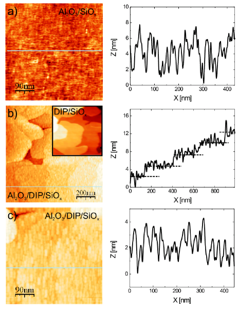
Fig. 1(b) shows an AFM image of a 681 Å thick aluminum oxide film deposited under similar sputtering conditions on top of a DIP film of 317 Å thickness. The inset shows a contact mode AFM image of an uncapped DIP film with its characteristic topography with terraces of monomolecular (ca. 16.5 Å) step height. The corresponding line scan reveals the surface morphology of aluminum oxide/DIP.
For the Al2O3/DIP system (Fig. 1(b)) the terraced structure of the underlying DIP film can still be recognized which implies that the Al2O3 surface roughness exhibits a certain degree of correlation with the DIP surface roughness. A closer look at the morphology of the aluminum oxide layer on a DIP terrace (Fig. 1(c)) exhibits a granular structure as could already be seen on the Al2O3/SiOx system (Fig. 1(a)). The aluminum oxide film thus reflects some features of the underlying substrates – the relatively flat native silicon oxide and the terraced DIP – in addition to its ’inherent’ graininess.
Roughness evolution of Al2O3/SiOx and Al2O3/DIP – X-ray reflectivity
From the X-ray reflectivity measurements the out-of-plane structure is probed and information on the film thickness, the electron density and interface roughness can be extracted. Aluminum oxide films of thicknesses ranging from ca. 116 Å to 5800 Å were prepared on both substrates. The experimental data of X-ray reflectivity measurements and fits using the Parratt formalism parratt_pr54 are displayed in Fig. 2(a) for Al2O3/SiOx and in Fig. 2(b) for Al2O3/DIP. The X-ray reflectivity curves are offset for clarity. The specular signal was obtained by subtracting the off-specular diffuse signal from the measured intensity. The inset in Fig. 2(b) shows the reflectivity of the 166 Å thick Al2O3/DIP film including the first order DIP Bragg reflection at Å-1.
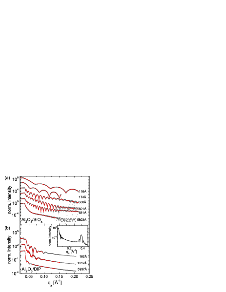
The specular X-ray reflectivity curves show pronounced thickness oscillations (Kiessig fringes) indicating well-defined interfaces (in terms of interface roughness).222The reflectivity curve for 5800 Å aluminum oxide on SiOx in Fig. 2(a) shows some oscillations which do not correspond to the thickness oscillations of a 5800 Å thick aluminum oxide film. During preparation of this specific film the sputtering process was interrupted to cool down the sputtering target. After restarting sputtering the preparation conditions might have changed slightly. The reflectivity curve could be fitted by using a model with two aluminum oxide films of slightly different electron density but the total film thickness being ca. 5800 Å. For all films no signature of crystalline aluminum oxide could be found at higher scattering angles, i.e., at the position of Bragg reflections of -Al2O3 at Å-1 and Å-1. From the fitting of the X-ray data the film thickness, the electron density and the film-substrate roughness as well as the film surface roughness was determined.parratt_pr54
IV Analysis and Discussion
For many systems prepared by different deposition methods the imperfection of a given layer is transferred fully or partly to the subsequent layers.schlomka_prb95 A simple way of taking into account the effect of vertical correlations between the interfaces in our samples is to ’renormalize’ the roughness of the aluminum oxide film by the rms roughness of the underlying substrate, according toholy_bk
| (2) |
where corresponds to the roughness of the underlying film/substrate, i.e. DIP or SiOx.
Aluminum oxide on SiOx
In Fig. 3(a) the roughness evolution of sputtered aluminum oxide films deposited on silicon oxide is displayed in a - plot as a function of the film thickness (open circles). The slope of a linear fit to the data corresponds to a roughness exponent of . The roughness of the silicon oxide substrate was 4 Å as determined from measurements on the clean substrate. When the aluminum oxide roughness is corrected for the relatively small roughness of the native silicon oxide substrate using Eq. (2) a roughness exponent of is obtained (see Fig. 3(b)).
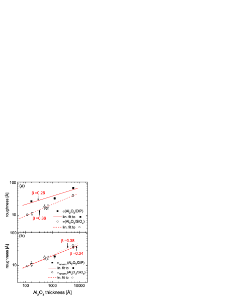
This result has to be compared to the wide range of experimental studies of different materials deposited by different techniques. For instance, for thermal evaporation of Fe on Fe(001)he_prl92 and for vapor deposited Ag on silicon substratesthompson_prb94 a scaling exponent of has been obtained, while for sputter-deposited Au films on Si(111) (at 300 K) and (at 200 K) you_prl93 and for sputtered Mo films on Si(111) was reportedjun_epl98 . For aluminum nitride (AlN) films deposited by reactive-sputtering on Si(100) substrates was foundauger_jap05 while for sputtered SnO2 films on glass substrates a growth exponent of approximately 0.3 is reported. lindstroem_tsf01
The theoretical predictions for depend on the assumptions of the specific model.krug_advp97 Obviously, the various values show that for different materials, substrate temperatures and deposition techniques different growth mechanisms are dominating.
Aluminum oxide on DIP/SiOx
The roughness of aluminum oxide films of different thickness deposited on top of DIP films is plotted in Fig. 3(a) (filled squares) and an uncorrected growth exponent of is extracted. Given the large roughness of the substrate (the DIP film) the renormalization is essential.
Table 1 summarizes the thickness and roughness of the aluminum oxide and DIP films and the renormalized aluminum oxide roughness . As shown in Fig. 3(b) the renormalized aluminum oxide roughness yields a scaling exponent of 333We note that this values arise under the present specific sputtering conditions employed in this study, but is not necessarily universal. We rather expect it to change with sputtering power, geometry, argon gas pressure and other experimental parameters. – a value which is remarkably similar to the scaling exponent determined for the Al2O3/SiOx system. With the similar morphology of aluminum oxide on silicon oxide substrates (Fig. 1(a)) and on a single terrace of DIP (Fig. 1(c)), it appears that the growth and structure of the aluminum oxide films is similar on both kinds of substrates.
| [Å] | [Å] | [Å] | [Å] | [Å] |
|---|---|---|---|---|
| 166.4 | 27.5 | 344.6 | 25.0 | 11.5 |
| 1212.4 | 34.0 | 351.5 | 28.0 | 19.3 |
| 5937.6 | 71.7 | 402.0 | 60.2 | 38.9 |
We note that at least in the initial stage , i.e. that the ’starting roughness’ provided by DIP is the dominating contribution to the aluminum oxide roughness. Because of the pronounced and well-developed terrace structure of DIP the renormalization yields the small ’local’ roughness () on top of a given terrace, whereas the ’global’ roughness () of aluminum oxide contains the ’terrace-to-terrace’ contribution of the underlying DIP film. Thus, at least for not too thick films, the renormalization procedure appears to be a sensible approach. The remarkable observation is the similarity in the roughness exponent despite the very different chemical nature of the two substrates and the substantially lower surface energy of DIP compared to silicon oxide.
V Summary
We have studied the structure and morphology of aluminum oxide films deposited on silicon oxide and organic films of DIP. From the analysis of the X-ray reflectivity measurements we found a roughness exponent of for aluminum oxide films on silicon oxide. The growth exponent was also determined for sputter deposited aluminum oxide films on DIP films. The simple renormalization approach of Eq. (2) works remarkably well. After renormalizing in the Al2O3/DIP system a similar -exponent of 0.34 as for the Al2O3/SiOx system () was obtained. The similar growth exponents and the AFM images of the Al2O3/SiOx and Al2O3/DIP systems suggest that the growth and local structure of aluminum oxide exhibit similarities despite the different chemical nature of the substrates.
Acknowledgements
We acknowledge support by the Deutsche Forschungsgemeinschaft (DFG) within the Focus Programme on organic field effect transistors and support from the Engineering and Physical Sciences Research Council (EPSRC). We are grateful to the FZ Karlsruhe and the ANKA synchrotron, to N. Kasper for his technical assistance and to H. Paulus and W. Bolse from the Institut für Strahlenphysik for the RBS measurements.
References
- (1) W. H. Rippard, A. C. Perrella, F. J. Albert, and R. A. Buhrman, Phys. Rev. Lett. 88 (2002) 046805.
- (2) N. P. Padture, M. Gell, and E. H. Jordan, Science 296 (2002) 280 .
- (3) A. Stierle, F. Renner, R. Streitel, H. Dosch, W. Drube, and B. C. Cowie, Science 303 (2004) 1652 .
- (4) S.-H. K. Park, J. Oh, C.-S. Hwang, J.-I. Lee, Y. S. Yang, H. Y. Chu, and K.-Y. Kang, ETRI J. 27 (2005) 545 .
- (5) A. B. Chwang, M. A. Rothman, S. Y. Mao, R. H. Hewitt, M. S. Weaver, J. A. Silvernail, K. Rajan, M. Hack, J. J. Brown, X. Chu, L. Moro, T. Krajewski, and N. Rutherford, Appl. Phys. Lett. 83 (2003) 413 .
- (6) M. Voigt and M. Sokolowski, Mater. Sci. Eng. B 109 (2004) 99 .
- (7) J. Krug, Adv. Phys. 46 (1997) 139.
- (8) A. Pimpinelli and J. Villain, Physics of Crystal Growth, Monographs and Texts in Statistical Physics (Cambridge University Press, 1999).
- (9) A.-L. Barabási and H. E. Stanley, Fractal Concepts in Surface Growth (Cambridge University Press, 1995).
- (10) F. Family and T. Vicsek, J. Phys. A: Math. Gen. 18 (1985) L75 .
- (11) F. Family, Physica A 168 (1990) 561 .
- (12) F. Family, J. Phys. A: Math. Gen. 19 (1986) L441 .
- (13) M. Kardar, G. Parisi, and Y.-C. Zhang, Phys. Rev. Lett. 56 (1986) 889 .
- (14) E. D. Wolf and J. Villain, Europhys. Lett. 13 (1990) 389 .
- (15) R. Jullien and R. Botet, J. Phys. A: Math. Gen. 18 (1985) 2279 .
- (16) J. Krug and P. Meakin, Phys. Rev. Lett. 66 (1991) 703 .
- (17) Z.-W. Lai and S. D. Sarma, Phys. Rev. Lett. 66 (1991) 2348 .
- (18) L.-H. Tang and T. Nattermann, Phys. Rev. Lett. 66 (1991) 2899 .
- (19) A. C. Dürr, F. Schreiber, K. A. Ritley, V. Kruppa, J. Krug, H. Dosch, and B. Struth, Phys. Rev. Lett. 90 (2003) 016104.
- (20) Y.-L. He, H.-N. Yang, T.-M. Lu, and G.-C. Wang, Phys. Rev. Lett. 69 (1992) 3770 .
- (21) C. Thompson, G. Palasantzas, Y. P. Feng, S. K. Sinha, and J. Krim, Phys. Rev. B 49 (1994) 4902.
- (22) H. You, R. P. Chiarello, H.-K. Kim, and K. G. Vandervoort, Phys. Rev. Lett. 70 (1993) 2900 .
- (23) J. Wang, G. Li, P. Yang, M. Cui, X. Jiang, B. Dong, and H. Liu, Europhys. Lett. 42 (1998) 283 .
- (24) M. A. Auger, L. Vázquez, O. Sánchez, M. Jergel, R. Cuerno, and M. Castro, J. Appl. Phys. 97 (2005) 123528 .
- (25) T. Lindström, J. Isidorsson, and G. A. Niklasson, Thin Solid Films 401 (2001) 165 .
- (26) G. W. Collins, S. A. Letts, E. M. Fearon, R. L. McEachern, and T. P. Bernat, Phys. Rev. Lett. 73 (1994) 708.
- (27) H.-J. Ernst, F. Fabre, R. Folkerts, and J. Lapujoulade, Phys. Rev. Lett. 72 (1994) 112.
- (28) A. C. Dürr, F. Schreiber, M. Münch, N. Karl, B. Krause, V. Kruppa, and H. Dosch, Appl. Phys. Lett. 81 (2002) 2276.
- (29) S. Kowarik, A. Gerlach, S. Sellner, F. Schreiber, L. Cavalcanti, and O. Konovalov, Phys. Rev. Lett. 96 (2006) 125504.
- (30) A. C. Dürr, F. Schreiber, M. Münch, B. Krause, V. Kruppa, and H. Dosch, Adv. Mater. 14 (2002) 961.
- (31) S. Sellner, A. Gerlach, F. Schreiber, M. Kelsch, N. Kasper, H. Dosch, S. Meyer, J. Pflaum, M. Fischer, and B. Gompf, Adv. Mater. 16 (2004) 1750.
- (32) S. Sellner, A. Gerlach, F. Schreiber, M. Kelsch, N. Kasper, H. Dosch, S. Meyer, J. Pflaum, M. Fischer, B. Gompf, and G. Ulbricht, J. Mater. Res. 21 (2006) 455.
- (33) S. Meyer, S. Sellner, F. Schreiber, H. Dosch, G. Ulbricht, M. Fischer, B. Gompf, and J. Pflaum, Mater. Res. Soc. Symp. Proc. 965E (2007) 6.
- (34) L. G. Parratt, Phys. Rev. 95 (1954) 359.
- (35) J.-P. Schlomka, M. Tolan, L. Schwalowsky, O. H. Seeck, J. Stettner, and W. Press, Phys. Rev. B 51 (1995) 2311.
- (36) V. Holý, U. Pietsch, and T. Baumbach, High-Resolution X-Ray Scattering from Thin Films and Multilayers (Springer Berlin, Heidelberg, New York, 1999).