Highly sensitive and broadband carbon nanotube radio-frequency single-electron transistor
Abstract
We have investigated radio-frequency single-electron transistor operation of single-walled carbon nanotube quantum dots in the strong tunneling regime. At a temperature of K and with carrier frequency MHz, we reach a charge sensitivity of over a bandwidth of MHz. Our results indicate a gain-bandwidth product of , which is by one order of magnitude better than for typical RF-SETs.
pacs:
PACS numbers: 67.57.Fg, 47.32.-yI Introduction
The single-electron transistor (SET) is a highly sensitive electrometer, conventionally based on sequential tunneling of electrons in the Coulomb blockade regime. 1 Unfortunately, the -time due to cable capacitance ( nF) and device resistance () limits the bandwidth to a few kHz. This is a major drawback for the direct application of SETs as it limits the operation to a regime where -noise is strong, either due to background charge noise, 2 or to variations in the tunneling resistance. 3
The limitation on the frequency bandwidth can be bypassed using microwave techniques for reading out the real part of the SET impedance. In these so called RF-SETs, 4 an -circuit is used to transform the high impedance of the SET to a high-frequency setup with a characteristic impedance of . The transformation is frequency selective, and a good match is obtained only over a frequency range , where is the resonant frequency of the matching circuit, and under fully matched conditions. Typical charge sensitivities of RF-SETs amount to over a signal bandwidth of MHz. 4
In order to improve the performance of RF-SETs, the operating regime has to be brought from sequential tunneling to co-tunneling, i.e., from the weak to the strong tunneling regime. 5 The energy sensitivity including back action noise has been estimated to be in the sequential tunneling regime. 6 In the co-tunneling regime, the sensitivity is expected to approach . 5 Another benefit of the strong tunneling regime is that a wider bandwidth can be obtained as the -factor can be made smaller. However, the effective Coulomb energy diminishes rapidly with lowering resistance of the tunnel barriers. This behavior has been summarized for single junctions by Wang et al. 7 They find, e.g., that for k. Provided that , the strong tunneling SETs are expected to operate well as RF-SETs. 8 This regime of operation has been strived for by Brenning et al. 9 They managed to fabricate Al/AlOx tunnel junction SETs with K, and a total resistance of k. For the charge sensitivity, they reached at 4.2 K, which is the best liquid helium result obtained so far.
Single-walled carbon nanotubes (SWCNTs) provide an alternative approach to the metallic SETs in the strong tunneling regime. The first reports on single-electron charging effects in individual tubes and bundles were published in 1997. 10, 11 Charging energies of about meV were quickly observed. 12 Since then, contacting techniques have greatly improved, and impedances of – k can be rather routinely obtained, e.g., using Pd contacts. 13 SWCNTs with large are very promising for RF-SETs, especially since their shot noise has been found to be well below the Schottky value. 14
In this article, we report on RF-SETs made from SWCNTs in the strong tunneling regime. We find a charge sensitivity of at K, which nearly equals that obtained by Brenning et al. 9 Compared with previous carbon nanotube RF-SETs,15, 16, 17 the improvement is by a factor ranging from 7 to 200. In combination with a bandwidth of MHz, our results represent a considerable improvement for broadband charge sensing, e.g., for fast read-out of single-electron devices such as quantum dots.
II Device fabrication and experimental setup
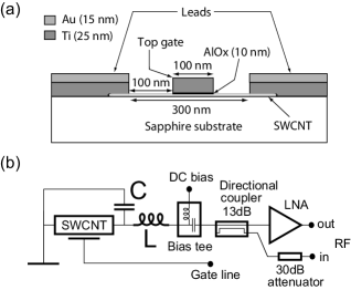
Our SWCNTs are grown from patterned catalyst islands, following the approach of Kong et al. 18, 19 RF-SET operation necessitates the use of insulating substrates in order to minimize the shunt capacitance. We use sapphire for lower losses and charge noise compared to conventional Si/SiO2. The chemical vapor deposition (CVD) takes place in a ceramic tube furnace from a gas mixture of Ar, H2, and CH4 at . After growth, pairs of / nm Ti/Au contacts, m apart, are defined between the catalyst islands by electron beam lithography. A central top-gate, m wide, is deposited between the contacts. Under the actual nm Ti gate, an insulating barrier is formed by five nm Al layers, each oxidized min at atmosphere. Finally, we deposit a Cr/Au mask with m bond-pads. The final device layout is illustrated in Fig. 1(a).

A schematic of the low-temperature measurement setup is shown in Fig. 1(b).21 The sample connects to an -circuit, formed by the inductance nH of a surface mount inductor and the bond-wires, and the parasitic capacitance pF of the bond-pads. The circuit is connected to a coplanar transmission line with a surface mount bias-tee that couples the DC-bias and RF-signal. The top-gate is connected to a separate coaxial line for high-bandwidth modulation. We use a home-made low-noise amplifier with a frequency range of – MHz. 20 The RF-input is coupled to the coaxial line through a dB directional coupler and a dB attenuator that reduces the noise from room temperature. The RF-output is detected in a fashion dependent of the goal of the measurement: 1) by a spectrum analyzer to investigate the carrier modulation spectra, or 2) by mixer demodulation for homodyne detection at a particular frequency.
III Results and discussion
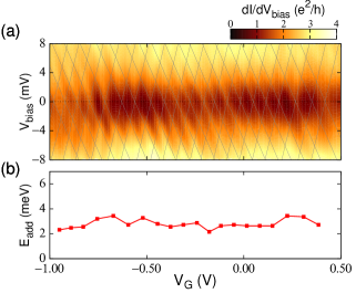
Fig. 2(a) shows the differential conductance () versus gate and bias voltages (, ). For mV, – , indicating a high-quality SWCNT sample with highly transparent contacts. However, there is a clear but smooth Coulomb modulation pattern at . As such, the sample behaves as a SET in the strong tunneling regime. By tracing the Coulomb diamonds, we find the addition energies , with Coulomb energy and level spacing . The values in Fig. 2(b) cover the range – meV, which sets an upper bound of K, corresponding to a total capacitance of the SET island of aF. From the gate modulation and slopes of the diamonds in Fig. 2(a), we estimate that the gate capacitance aF.

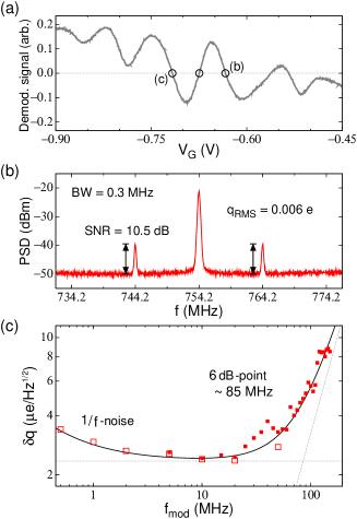
For RF-SET operation, the optimum operating point was found by searching for points of perfect matching, i.e., vanishing reflection at the resonance frequency MHz. The signal was homodyne detected by mixer, and the phase was tuned to be sensitive only to the real part of the SET impedance. We found three points around – V with maximum differential response, coinciding with perfect matching (Fig. 3(a)). Using a spectrum analyzer, the input carrier power was tuned to obtain maximum signal-to-noise ratio of the sidebands at , while keeping a small gate-charge modulation of at MHz (Fig. 3(b)). The signal-to-noise ratio (SNR) of both sidebands yields a charge sensitivity of , corresponding to an uncoupled energy sensitivity of . The frequency response was mapped out by repeating the sensitivity measurement over a range of modulation frequencies of – MHz (Fig. 3(c)). We found a bandwidth of and observed that -noise only contributes significantly below – MHz.

Optimization of RF-SET sensitivity has been treated in several papers. 22, 23, 24, 25 The ultimate shot noise limited sensitivity was found in Ref. 21 to be
| (1) |
which in our case ( k, aF) amounts to . When the noise of the amplifier dominates the performance, the sensitivity scales with the noise amplitude and the differential response of the RF reflectance () as
| (2) |
where denotes the noise temperature of the amplifier and the amplitude of the RF carrier signal. In our case, the amplitude over the SET is mV at perfect matching. In Ref. 23, an approximation of Eq. (2) was found from the orthodox theory as
| (3) |
with and in units of K, and . Assuming that heating does not play a significant role, we estimate from Eq. (3) that , taking K, k, k, and K. All of these estimates are based on the classical orthodox theory for Coulomb blockade, 1 which is only valid in the weak tunneling regime. However, as discussed above, we are in the strong tunneling regime. One way around this issue is simply to adopt the effective charging energy , calculated by Wang et al.7 Then the estimate for the charge sensitivity becomes , which agrees well with the measured value. In making our estimates, we have neglected the effects of quantum level spacing (see discussion in Ref. 30).
IV Conclusions
We have shown that a SWCNT quantum dot in the strong tunneling regime can be operated as an excellent RF-SET at liquid helium temperature ( K). We obtain a charge sensitivity of , which is nearly as good as the best Al/AlOx results.9 It represents an enhancement of at least a factor of 7 compared with previous carbon nanotube RF-SETs.15, 16, 17 Very recently, comparable sensitivities were achieved with other types of SETs: 1) InAs/InP heterostructured nanowires,26 and 2) electrostatically defined Si quantum dots.27
With a bandwidth of MHz, our gain-bandwidth product amounts to , where gain is defined as . That is by more than one order of magnitude better than for typical RF-SETs.4 Therefore, SWCNT based RF-SETs may have value in applications where high speed is needed. One possible application is for charge sensing on quantum dots in the context of quantum computing. Here, the coupling to a nearby quantum dot structure, e.g., another nanotube, could be achieved via an antenna gate as it was recently demonstrated with SiGe nanowires.28
The best way to enhance the sensitivity further would be to lower the temperature so the Coulomb modulation is fully developed. For Al/AlOx junction SETs, the improvement at 40 mK was in the superconducting state and in the normal state. 9 To improve the bandwidth, the only option is to increase the resonance frequency of the -circuit. The limit set by the Bode-Fano criterium states that the maximum achievable bandwidth is , which in our case amounts to MHz.
Acknowledgements.
We wish to acknowledge H. I. Jørgensen, K. Grove-Rasmussen, T. Heikkilä, M. Paalanen, P. E. Lindelof, and B. Placais for fruitful discussions. This work was supported by the Academy of Finland grant 213496 and by the EU under contract FP6-IST-021285-2.References
- 1 See, e.g., K. K. Likharev, Proc. IEEE 87, 606 (1999).
- 2 B. Starmark, T. Henning, T. Claeson, P. Delsing, and A. N. Korotkov, J. Appl. Phys. 86, 2132 (1999).
- 3 V. Krupenin, D. Presnov, M. Savvateev, H. Scherer, A. Zorin, and J. Niemeyer, J. Appl. Phys. 84, 3212 (1998).
- 4 R. J. Schoelkopf, P. Wahlgren, A. A. Kozhevnikov, P. Delsing, and D. E. Prober, Science 280, 1238 (1998).
- 5 D. Averin, in Macroscopic Quantum Coherence and Quantum Computing, edited by D. V. Averin, B. Ruggiero, and P. Silvestrini (Kluwer, New York, 2001) pp. 399–408; arXiv:cond-mat/0010052.
- 6 M. H. Devoret, R. J. Schoelkopf, Nature 406, 1039 (2000)
- 7 X. Wang, R. Egger and H. Grabert, Europhys. Lett. 38, 545 (1997).
- 8 P. Wahlgren, Ph.D. thesis, Chalmers University of Technology, unpublished (1998).
- 9 H. Brenning, S. Kafanov, T. Duty, S. Kubatkin and P. Delsing, J. Appl. Phys. 100, 114321 (2006).
- 10 S. J. Tans, M. H. Devoret, H. Dai, A. Thess, R. S. Smalley, L. J. Geerlings, and C. Dekker, Nature (London) 386, 474 (1997).
- 11 M. Bockrath, D. H. Cobden, P. L. McEuen, N. G. Chopra, A. Zettl, A. Thess, and R. E. Smalley, Science 275, 1922 (1997).
- 12 J. Nygard, D. H. Cobden, M. Bockrath, P. L. McEuen, and P. E. Lindelof, Applied Physics A 69, 297 (1999).
- 13 A. Javey, J. Guo, Q. Wang, M. Lundstrom, and H. Dai, Nature 424, 654 (2003).
- 14 F. Wu, P. Queipo, A. Nasibulin, T. Tsuneta, T. H. Wang, E. Kauppinen and P. J. Hakonen, Phys. Rev. Lett. 99, 156803 (2007).
- 15 L. Roschier, M. Sillanpää, W. Taihong, M. Ahlskog, S. Iijima, and P. Hakonen, J. Low Temperature Phys. 136, 465 (2004).
- 16 M. J. Biercuk, D. J. Reilly, T. M. Buehler, V. C. Chan, J. M. Chow, R. G. Clark, and C. M. Marcus, Phys. Rev. B 73, 201402 (2006).
- 17 Y. Tang, I. Amlani, A. O. Orlov, G. L. Snider, and P. J. Fay, Nanotech. 18, 445203 (2007).
- 18 J. Kong, H. T. Soh, A. M. Cassell, C. F. Quate, and H. Dai, Nature 395, 878 (1998).
- 19 K. Grove-Rasmussen, H. I. Jørgensen, and P. E. Lindelof, Proceeding Int. Symp. on Mesoscopic Superconductivity and Spintronics 2006, NTT BRL, Atsugi, Japan, World Scientific Publishing (2007).
- 20 L. Roschier and P. Hakonen, Cryogenics 44, 783 (2004).
- 21 F. Wu, L. Roschier, T. Tsuneta, M. Paalanen, T. H. Wang, and P. Hakonen, AIP Proc. 850, 1482 (2006).
- 22 A. N. Korotkov and M. A. Paalanen, Appl. Phys. Lett. 74, 4052 (1999).
- 23 L. Roschier, P. Hakonen, K. Bladh, P. Delsing, K. W. Lehnert, L. Spietz, and R. J. Schoelkopf, J. Appl. Phys. 95, 1274 (2004).
- 24 V. O. Turin and A. N. Korotkov, App. Phys. Lett. 83, 2898 (2003).
- 25 V. O. Turin and A. N. Korotkov, Phys. Rev. B 69, 195310 (2004).
- 26 H. A. Nilsson, T. Duty, S. Abay, C. Wilson, J. B. Wagner, C. Thelander, P. Delsing, and L. Samuelson, Nano Lett. 8, 872 (2008).
- 27 S. J. Angus, A. J. Ferguson, A. S. Dzurak, and R. G. Clark, Appl. Phys. Lett. 92, 112103 (2008).
- 28 Y. Hu, H. O. H. Churchill, D. J. Reilly, J. Xiang, C. M. Lieber, and C. M. Marcus, Nature Nanotech. 2, 622 (2007).
- 29 C. W. J. Beenakker, Phys . Rev. B 44, 1646 (1991).
- 30 By studying the Coulomb diamond pattern around the optimum sensitivity we deduce that and . This suggests that we are in the quantum Coulomb blockade regime (QCB), where and only few levels are involved in transport. However, comparing the conductance peak line-shapes around optimum sensitivity with theory 29, we find deviations between the experimental data and QCB predictions. From the experimental data we get at peak maximum and as optimum transconductance. These values should be compared to and as predicted by theory. Also the predictions from the metallic Coulomb blockade regime with and are deviating, but the peak maximum is close to the measured. This discrepancy is explained by the fact that we are in the strong tunneling regime with which broadens the energy levels. Since we still have strong Coulomb blockade we are not quite in the Breit-Wigner limit, but rather in an intermediate regime which behaves closest to the strong tunneling description.