Radiation Hardness Studies in a CCD with
High-Speed Column Parallel Readout
André Sopczak
Lancaster University, UK; on behalf of the LCFI Collaboration
Abstract
Abstract
Charge Coupled Devices (CCDs) have been successfully used in several high energy physics experiments over the past two decades. Their high spatial resolution and thin sensitive layers make them an excellent tool for studying short-lived particles. The Linear Collider Flavour Identification (LCFI) collaboration is developing Column-Parallel CCDs (CPCCDs) for the vertex detector of the International Linear Collider (ILC). The CPCCDs can be read out many times faster than standard CCDs, significantly increasing their operating speed. The results of detailed simulations of the charge transfer inefficiency (CTI) of a prototype CPCCD are reported and studies of the influence of gate voltage on the CTI described. The effects of bulk radiation damage on the CTI of a CPCCD are studied by simulating the effects of two electron trap levels, 0.17 and 0.44 eV, at different concentrations and operating temperatures. The dependence of the CTI on different occupancy levels (percentage of hit pixels) and readout frequencies is also studied. The optimal operating temperature for the CPCCD, where the effects of the charge trapping are at a minimum, is found to be about 230 K for the range of readout speeds proposed for the ILC. The results of the full simulation have been compared with a simple analytic model.
I Introduction
Particle physicists worldwide are working on the design of a high energy collider of electrons and positrons (the International Linear Collider or ILC) which could be operational sometime around 2019. Any experiment exploiting the ILC will require a high performance vertex detector to detect and measure short-lived particles, yet be tolerant to radiation damage for its anticipated lifetime. One candidate is a set of concentric cylinders of Charge-Coupled Devices (CCDs), read out at a frequency of around 50 MHz.
It is known that CCDs suffer from both surface and bulk radiation damage. However, when considering charge transfer losses in buried channel devices only bulk traps are important. These defects create energy levels (traps) between the conduction and valence band, and electrons are captured by them. These electrons are also emitted back to the conduction band after a certain time.
It is usual to define the Charge Transfer Inefficiency (CTI) as the fractional loss of charge after transfer across one pixel. An initial charge after being transported across pixels is reduced to . For CCD devices containing many pixels, CTI values around 10-5 are important. Previous results for a CCD with sequential readout have recently been reported [1]. The expected background rate at the future ILC near the interaction point leads to radiation damage in the CCD detector. We simulated the charge transfer in a CPCCD (Column-Parallel CCD) using the trap concentrations listed in Fig. 1. They correspond to about 3 years of operation for the 0.17 eV traps and several more years for the 0.44 eV traps.
| () | () | |
|---|---|---|
| 0.17 | ||
| 0.44 |
II Simulations
The UK Linear Collider Flavour Identification (LCFI) collaboration [2] has been studying a CCD with high-speed (50 MHz) column-parallel readout produced by e2V Technologies. It is a two-phase buried-channel CCD with 20 m square pixels.
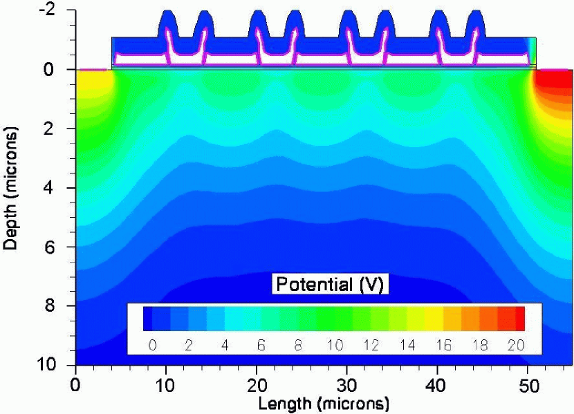
Simulations of a simplified model of this device have been performed with the ISE-TCAD package (version 7.5), particularly the DESSIS program (Device Simulation for Smart Integrated Systems). The simulation is essentially two dimensional and assumes a 1 m device thickness (width) for calculating densities. The overall length and depth are 55 m and 20 m respectively (Fig. 1).
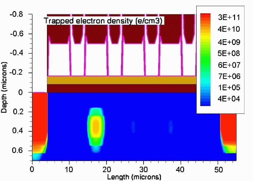
Parameters of interest are the readout frequency, up to 50 MHz, and the operating temperature between 130 K and 300 K although simulations have been performed up to 440 K. The charge in transfer and the trapped charge are shown in Fig. 2.
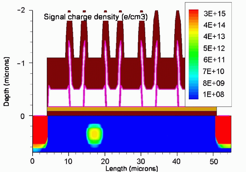
Charge Transfer Inefficiency is a measure of the fractional loss of charge from a signal packet as it is transferred over a pixel, or two gates. After DESSIS has simulated the transfer process, a 2D integration of the trapped charge density distribution is performed independently to give the total charge under each gate.
This CTI study, at nominal clock voltage, focuses only on the bulk traps with energies 0.17 eV and 0.44 eV below the bottom of the conduction band. These will be referred to simply as the 0.17 eV and 0.44 eV traps. The 0.17 eV trap is an oxygen-vacancy defect, referred to as an A-centre defect. The 0.44 eV trap is a phosphorus-vacancy defect, an E-centre defect, as a result of the silicon being doped with phosphorus and a vacancy manifesting from the displacement of a silicon atom bonded with a phosphorus atom [3].
III Simulation Results
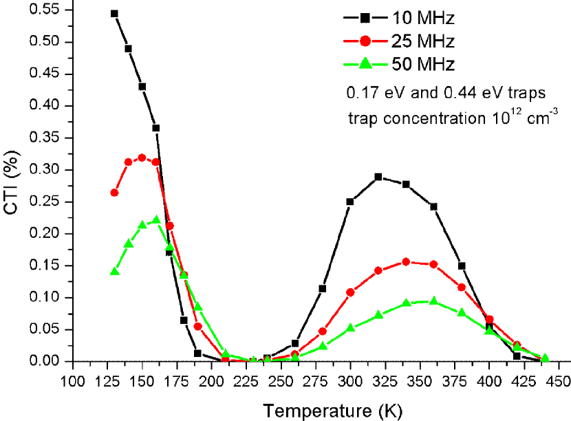
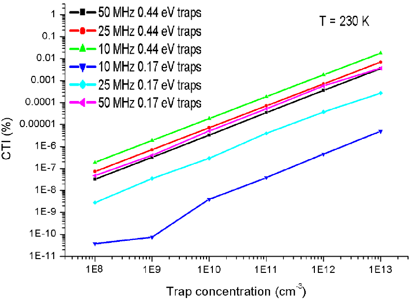
The CTI dependence on temperature and readout frequency was explored and Figure 3 shows the CTI for simulations with partially filled 0.17 eV and 0.44 eV traps at different frequencies for temperatures between 130 K and 440 K, with a nominal clock voltage of 3 V. The CTI value depends linearly on the trap concentration for a large concentration variation as also shown in Fig. 3.
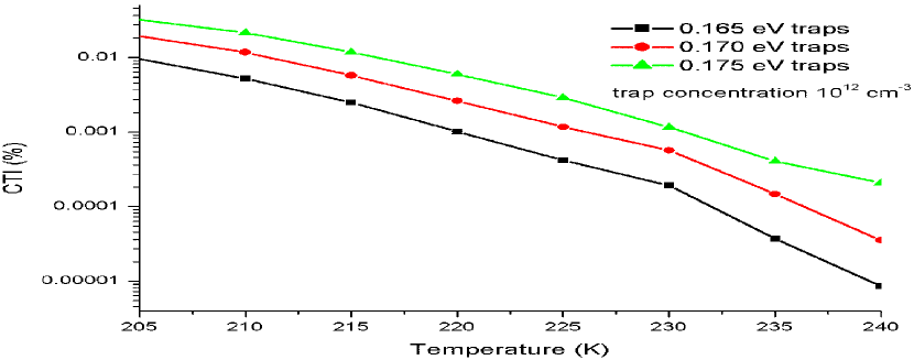
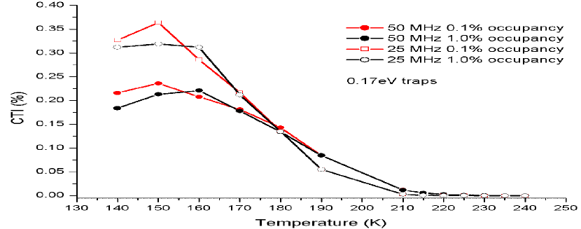
The CTI values for a variation of the 0.17 eV trap level by 0.005 eV and for 0.1% and 1% hit (pixel) occupancy are shown in Fig. 4. Figure 5 shows the results of a study of a clock voltage induced CTI in order to find the optimum clock voltage with a low power consumption and keeping the CTI at an acceptable level.
IV Comparisons with an Analytic Model
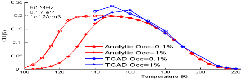
The motivation for introducing an analytic model is to understand the underlying physics through making comparisons with the TCAD simulations. This might then allow predictions of CTI for other CCD geometries without requiring a full simulation. A simple analytic model [1] has been adapted to the CPCCD characteristics. The analytic model gives very similar results as shown in Figs. 3 and 4. Figure 6 compares the full TCAD simulation for 0.17 eV traps and clocking frequency of 50 MHz to the analytic model. It emphasises the good agreement between the model and full simulations111For temperatures below 140K the full simulation does not converge.. The variation of hit occupancy is studied and as expected at lower temperatures larger hit occupancy leads to lower CTI values as traps are filled to a higher level.

However, there are limitations with the analytic model. They could relate to a breakdown of the assumptions at high temperatures, to ignoring the precise form of the clock voltage waveform, or to ignoring the pixel edge effects.
V Conclusions and Outlook
The Charge Transfer Inefficiency (CTI) of a CCD with high-speed column parallel readout has been studied with a full simulation (ISE-TCAD DESSIS) and compared with an analytic model. The 0.17 eV and 0.44 eV trap levels have been implemented in the full simulation and variations of the CTI with respect to temperature and frequency have been analysed. At low temperatures ( K) the 0.17 eV traps dominate the CTI, whereas the 0.44 eV traps dominate at higher temperatures. Good agreement between simulations and an analytic model adapted to the CPCCD has been found. The optimum operating temperature for the CPCCD prototype in a high radiation environment is found to be about 230 K for clock frequencies in the range 10 to 50 MHz. Our prototype CPCCD has recently operated at 45 MHz and a test-stand for CTI measurements is in preparation. The development of a high-speed CCD vertex detector is on track as a vital part of a future ILC detector.
Acknowledgments
This work is supported by the Science and Technology Facilities Council (STFC) and Lancaster University. The Lancaster authors wish to thank Alex Chilingarov, for helpful discussions, and the particle physics group at Liverpool University, for the use of its computers.
References
- [1] A. Sopczak et al., IEEE Trans. Nucl. Sci., 54 (2007) 1429, and references therein.
- [2] LCFI collaboration homepage: http://hepwww.rl.ac.uk/lcfi
- [3] K. Stefanov et al., IEEE Trans. Nucl. Sci., 47 (2000) 1280.