Shot Noise in Graphene
Abstract
We report measurements of current noise in single- and multi-layer graphene devices. In four single-layer devices, including a p-n junction, the Fano factor remains constant to within upon varying carrier type and density, and averages between 0.35 and 0.38. The Fano factor in a multi-layer device is found to decrease from a maximal value of 0.33 at the charge-neutrality point to 0.25 at high carrier density. These results are compared to theories for shot noise in ballistic and disordered graphene.
Shot noise, the temporal fluctuation of electric current out of equilibrium, originates from the partial transmission of quantized charge Blanter00 . Mechanisms that can lead to shot noise in mesoscopic conductors include tunneling, quantum interference, and scattering from impurities and lattice defects. Shot noise yields information about transmission that is not available from the dc current alone.
In graphene Geim07 ; CastroNeto07 , a zero-gap two-dimensional semi-metal in which carrier type and density can be controlled by gate voltages Novoselov04 , density-dependent shot-noise signatures under various conditions have been investigated theoretically Tworzydlo06 ; Cheianov06 . For wide samples of ballistic graphene (width-to-length ratio ) the Fano factor, , i. e., the current noise normalized to the noise of Poissonian transmission statistics, is predicted to be 1/3 at the charge-neutrality point and in both electron (n) and hole (p) regimes Tworzydlo06 . The value is predicted for shot noise across a ballistic p-n junction Cheianov06 . For strong, smooth “charge-puddle” disorder, theory predicts both at and away from the charge-neutrality point, for all SanJose07 . Disorder may thus have a similar effect on noise in graphene as in diffusive metals, where is universally Beenakker92 ; deJong92 ; Nazarov94 ; Steinbach96 ; Henny99 ; Schoelkopf97 regardless of shape and carrier density. Recent theory investigates numerically the evolution from a density-dependent to a density-independent with increasing disorder Lewenkopf07 . To our knowledge, experimental data for shot noise in graphene has not yet been reported.
This Letter presents an experimental study of shot noise in graphene at low temperatures and zero magnetic field. Data for five devices, including a locally-gated p-n junction, are presented. For three globally-gated, single-layer samples, we find in both electron and hole doping regions, with essentially no dependence on electronic sheet density, , in the range . Similar values are obtained for a locally-gated single-layer p-n junction in both unipolar (n-n or p-p) and bipolar (p-n or n-p) regimes. In a multi-layer sample, the observed evolves from at the charge-neutrality point to at .

Devices were fabricated by mechanical exfoliation of highly-oriented pyrolytic graphite Novoselov04 . Exfoliated sheets were deposited on a degenerately-doped Si substrate capped with of thermally grown . Regions identified by optical microscopy as potential single-layer graphene were contacted with thermally evaporated Ti/Au leads (5/40 ) patterned by electron-beam lithography. Additional steps in the fabrication of the p-n junction device are detailed in Ref. Williams07 . Devices were measured in two cryostats, one allowing dc (lock-in) transport measurements in fields perpendicular to the graphene plane, and another allowing simultaneous measurements of dc transport and noise Techniques06 near , but limited to .
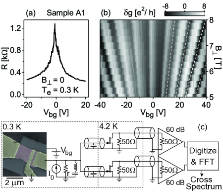
Differential resistance ( is the current, and is the source-drain voltage) of a wide, short sample [A1, ] is shown as a function of back-gate voltage at and in Fig. 1(a). While the width of the peak is consistent with A1 being single-layer graphene Novoselov05 ; Zhang05 , more direct evidence is obtained from the QH signature shown in Fig. 1(b). The grayscale image shows differential conductance as a function of and , following subtraction of the best-fit quadratic polynomial to at each setting to maximize contrast. Dashed lines correspond to filling factors , 10, 14, and 18, with and lever arm . Their alignment with local minima in identifies A1 as single-layer graphene McCann06 ; Martin07 . The Drude mean free path Rycerz06 , where , is found to be away from the charge-neutrality point using the conductivity [Fig. 2(a) inset].

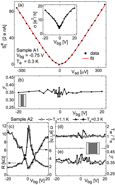
Current noise spectral density is measured using a cross-correlation technique described in Ref. Techniques06 [see Fig. 1(c)]. Following calibration of amplifier gains and electron temperature using Johnson noise thermometry (JNT) for each cooldown, the excess noise is extracted. for sample A1 is shown in Fig. 2(a). Linearity of at high bias indicates negligible extrinsic ( or telegraph) resistance fluctuations within the measurement bandwidth. For these data, a single-parameter fit to the scattering-theory form (for energy-independent transmission) Lesovik89 ; Buttiker92 ,
| (1) |
gives a best-fit Fano factor . Simultaneously measured conductance was independent of bias within (not shown) in the range used for the fit. Note that the observed quadratic-to-linear crossover agrees well with that in the curve fit, indicating weak inelastic scattering in A1 Steinbach96 ; Henny99 , and negligible series resistance (e. g., from contacts), which would broaden the crossover by reducing the effective across the sample.
Figure 2(b) shows similarly measured values for as a function of . is observed to remain nearly constant for . Over this density range, the average is with standard deviation . The estimated error in the best-fit at each setting is , comparable to the marker size and smaller than the variation in near , which we believe results from mesoscopic fluctuations of . Nearly identical noise results (not shown) were found for a similar sample (B), with dimensions and a QH signature consistent with a single layer.
Transport and noise data for a more square single-layer sample [A2, patterned on the same graphene sheet as A1, with dimensions ] at (solid circles) and (open circles) are shown in Figs. 2(c-e). At both temperatures, the conductivity shows and gives away from the charge-neutrality point. That these two values differ from those in sample A1 is particularly notable as samples A1 and A2 were patterned on the same piece of graphene. Results of fitting Eq. (1) to for sample A2 are shown in Figs. 2(d) and 2(e). To allow for possible broadening of the quadratic-to-linear crossover by series resistance and/or inelastic scattering, we treat electron temperature as a second fit parameter (along with ) and compare the best-fit value, , with the obtained from Johnson noise. Figure 2(d) shows tracking the calibrated at both temperatures. Small deviation of from unity near the charge-neutrality point at can be attributed to conductance variations up to in the fit range at these values of . As in sample A1, is found to be independent of carrier type and density over , averaging 0.37(0.36) with standard deviation 0.02(0.02) at K. Evidently, despite its different aspect ratio, A2 exhibits a noise signature similar to that of A1.
The lack of -dependence in suggests that bias-dependent electron heating in the metallic reservoirs Henny99 is negligible for our samples. This heating, originating from imperfect dissipation of the generated power , can affect shot noise measurements since these require several times the thermal voltage (here, ). In the presence of heating, fitting the excess noise to Eq. (1) overestimates . The nearly equal values of observed in A1 and A2 despite the factor difference in at comparable suggest that heating in the reservoirs is negligible HeatingNote .
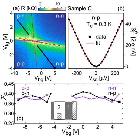
Transport and noise measurements for a single-layer graphene p-n junction Williams07 , sample C, are shown in Fig. 3. The color image in Fig. 3(a) shows differential resistance as a function of and local top-gate voltage . The two gates allow independent control of charge densities in adjacent regions of the device [see Fig. 3(c) inset]. In the bipolar regime, the best-fit shows little density dependence and averages 0.38, equal to the average value deep in the unipolar regime, and similar to results for the back-gate-only single-layer samples (A1, A2 and B). Close to charge neutrality in either region (though particularly in the region under the top gate), deviates from the form of Eq. (1) (data not shown). This is presumably due to resistance fluctuation near charge neutrality, probably due mostly to mobile traps in the insulator beneath the top gate.

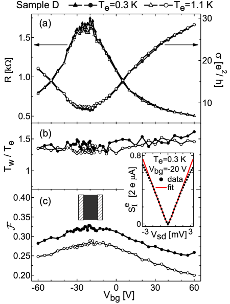
Measurements at and at for sample D, of dimensions , are shown in Fig. 4. A step height between and carbon surfaces measured by atomic force microscopy prior to electron-beam lithography Graf07 suggests this device is likely multi-layer. Further indications include the broad peak Zhang05a and the large minimum conductivity, at [Fig. 4(a)], as well as the absence of QH signature for at (not shown). Two-parameter fits of data to Eq. (1) show three notable differences from results in the single-layer samples [Figs. 4(b) and 4(c)]: First, shows a measurable dependence on back-gate voltage, decreasing from 0.33 at the charge-neutrality point to 0.25 at for ; Second, decreases with increasing temperature; Finally, is 1.3-1.6 instead of very close to 1. We interpret the last two differences, as well as the sublinear dependence of on (see Fig. 4 inset) as indicating sizable inelastic scattering Beenakker92 ; deJong92 in sample D. (An alternative explanation in terms of series resistance would require it to be density, bias, and temperature dependent, which is inconsistent with the independence of on and ).

Summarizing the experimental results, we find that in four single-layer samples, is insensitive to carrier type and density, temperature, aspect ratio, and the presence of a p-n junction. In one multi-layer sample, does depend on density and temperature, and shows a broadened quadratic-to-linear crossover and is sublinear in at high bias. We may now compare these results to expectations based on theoretical and numerical results for ballistic and disordered graphene.
Theory for ballistic single-layer graphene with gives a universal at the charge-neutrality point, where transmission is evanescent, and for , where propagating modes dominate transmission Tworzydlo06 . While the measured at the charge-neutrality point in samples A1 and B ( and , respectively) is consistent with this prediction, the absence of density dependence is not: is well within the range of carrier densities covered in the measurements. Theory Schomerus07 for ballistic graphene contacted with finite-density leads finds slight increments of from 1/3 at the charge-neutrality point, in agreement with this experiment. However, in this contact model remains density dependent. Theory for ballistic graphene p-n junctions Cheianov06 predicts , lower than the value observed in sample C in both p-n and n-p regimes. We speculate that these discrepancies likely arise from the presence of disorder. Numerical results for strong, smooth disorder SanJose07 predict a constant at and away from the charge-neutrality point for , consistent with experiment. However, the predicted value is lower than observed in all single-layer devices. Recent numerical simulations Lewenkopf07 of small samples () investigate the vanishing of carrier dependence in with increasing disorder strength. In the regime where disorder makes density-independent, the value is found to depend weakly on disorder strength and sample size.
Since theory for an arbitrary number of layers is not available for comparison to noise results in the multi-layer sample D, we compare only to existing theory for ballistic bi-layer graphene Snyman07 . It predicts over a much narrower density range than for the single layer, and abrupt features in at finite density due to transmission resonances. A noise theory beyond the bi-layer ballistic regime may thus be necessary to explain the observed smooth decrease of with increasing density in sample D.
We thank C. H. Lewenkopf, L. S. Levitov, and D. A. Abanin for useful discussions. Research supported in part by the IBM Ph.D. Fellowship program (L.D.C.), INDEX, an NRI Center, and Harvard NSEC.
References
- (1) Y. M. Blanter and M. Büttiker, Phys. Rep. 336, 1 (2000).
- (2) A. K. Geim and K. S. Novoselov, Nature Mater. 6, 183 (2007).
- (3) A. H. Castro Neto et al., arXiv:0709.1163 (2007).
- (4) K. S. Novoselov et al., Science 306, 666 (2004).
- (5) J. Tworzydło et al., Phys. Rev. Lett. 96, 246802 (2006).
- (6) V. V. Cheianov and V. I. Fal’ko, Phys. Rev. B 74, 041403(R) (2006).
- (7) P. San-Jose, E. Prada and D. S. Golubev, Phys. Rev. B 76, 195445 (2007).
- (8) C. W. J. Beenakker and M. Büttiker, Phys. Rev. B 46, 1889(R) (1992).
- (9) M. J. M. de Jong and C. W. J. Beenakker, Phys. Rev. B 46, 13400 (1992).
- (10) Y. V. Nazarov, Phys. Rev. Lett. 73, 134 (1994).
- (11) A. H. Steinbach, J. M. Martinis and M. H. Devoret, Phys. Rev. Lett. 76, 3806 (1996).
- (12) M. Henny et al., Phys. Rev. B 59, 2871 (1999).
- (13) R. J. Schoelkopf et al., Phys. Rev. Lett. 78, 3370 (1997).
- (14) C. H. Lewenkopf, E. R. Mucciolo and A. H. Castro Neto, arXiv:0711.3202 (2007).
- (15) J. R. Williams, L. DiCarlo and C. M. Marcus, Science 317, 638 (2007).
- (16) L. DiCarlo et al., Rev. Sci. Instrum. 77, 073906 (2006).
- (17) K. S. Novoselov et al., Nature 438, 197 (2005).
- (18) Y. Zhang et al., Nature 438, 201 (2005).
- (19) E. McCann and V. I. Fal’ko, Phys. Rev. Lett. 96, 086805 (2006).
- (20) J. Martin et al., Nature Phys. 4, 144 (2008).
- (21) A. Rycerz, J. Tworzydło and C. W. J. Beenakker, Europhys. Lett. 79, 57003 (2007).
- (22) G. B. Lesovik, Pis’ma Zh. Eksp. Teor. Fiz. 49, 513 (1989) [JETP Lett. 49, 592 (1989)].
- (23) M. Büttiker, Phys. Rev. B 46, 12485 (1992).
- (24) Effects of reservoir heating on noise have been observed in diffusive wires () with metallic contacts Henny99 . The generated power in our graphene samples is weaker by 1-3 orders of magnitude, which could explain why heating of the metallic contacts appears negligible in this experiment.
- (25) D. Graf et al., Phys. Rev. B 75, 245429 (2007).
- (26) Y. Zhang et al., Phys. Rev. Lett. 94, 176803 (2005).
- (27) H. Schomerus, Phys. Rev. B 76, 045433 (2007).
- (28) I. Snyman and C. W. J. Beenakker, Phys. Rev. B 75, 045322 (2007).