Electrically-driven phase transition in magnetite nanostructures
Abstract
Magnetite (Fe3O4), an archetypal transition metal oxide, has been used for thousands of years, from lodestones in primitive compassesMills:2004 to a candidate material for magnetoelectronic devices.Coey:2003 In 1939 VerweyVerwey:1939 found that bulk magnetite undergoes a transition at K from a high temperature “bad metal” conducting phase to a low-temperature insulating phase. He suggestedVerwey:1941 that high temperature conduction is via the fluctuating and correlated valences of the octahedral iron atoms, and that the transition is the onset of charge ordering upon cooling. The Verwey transition mechanism and the question of charge ordering remain highly controversial.Walz:2002 ; Garcia:2004 ; Huang:2006 ; Nazarenko:2007 ; Subias:2004 ; Rozenberg:2006 ; Piekarz:2006 Here we show that magnetite nanocrystals and single-crystal thin films exhibit an electrically driven phase transition below the Verwey temperature. The signature of this transition is the onset of sharp conductance switching in high electric fields, hysteretic in voltage. We demonstrate that this transition is not due to local heating, but instead is due to the breakdown of the correlated insulating state when driven out of equilibrium by electrical bias. We anticipate that further studies of this newly observed transition and its low-temperature conducting phase will shed light on how charge ordering and vibrational degrees of freedom determine the ground state of this important compound.
Strongly correlated electronic materials can exhibit dramatic electronic properties (e.g., high temperature superconductivity, metal-insulator transitions, and charge ordering) not present in simple systems with weaker electron-electron interactions. Such rich electronic phenomenology can result when electron-electron interactions, electron-phonon interactions, and electronic bandwidth are all of similar magnitude, as in magnetite.Gasparov:2000 VerweyVerwey:1939 found nearly seven decades ago that bulk magnetite, while moderately conductive at room temperature, undergoes a transition to a more insulating state below what is now called the Verwey temperature, K. Similar transitions are known in a number of materials.Imada:1998 ; Coey:2004 Above , Fe3O4 has an inverse-spinel structure of the form AB2O4, with tetrahedrally coordinated A sites occupied by Fe3+ and octrahedrally coordinated B sites of mixed valence, equally occupied by irons with formal and charges. Conduction at high temperatures has long been thought to be through fluctuating valences of the B sites, with the transition corresponding to some kind of B site charge ordering as decreases; concurrent is a first-order structural phase transition to an orthorhombic unit cell. This explanation remains controversial,Walz:2002 ; Garcia:2004 with experiments showing some charge disproportion or charge order (CO),Huang:2006 ; Nazarenko:2007 and others implying that the structural degrees of freedom drive the change in conductivity.Subias:2004 ; Rozenberg:2006 Recent theoretical progress has been made in understanding the complex interplay of charge and structural degrees of freedomLeonov:2006 ; Pinto:2006 , including a complete picture of the transition mechanism Piekarz:2006 with strongly correlated 3 Fe electrons acting to amplify electron-phonon couplings. Testing these ideas experimentally is of much interest.
In this Letter we report electronic transport measurements in magnetite at the nanoscale on both nanocrystals and single-crystal epitaxial thin films. Both types of devices exhibit striking electrically-driven hysteretic switching of the electronic conductance once sample temperatures are reduced below . The data clearly show that the transition is not the result of local heating above , but instead is an electrically-driven breakdown of the insulating state. We discuss possible explanations for this switching in the context of the general Verwey transition problem. While qualitatively similar resistive switching has been observed in other correlated oxide systemsAsamitsu:1997 ; Sawa:2004 , the phenomenon in Fe3O4 is a bulk effect with a mechanism distinct from these.
Two-terminal devices for applying voltages and measuring conduction at the nanoscale have been fabricated (see Methods) incorporating both Fe3O4 nanocrystalsYu:2004 (10-20 nm in diameter with oleic acid coating) and single-crystal thin films (40-60 nm thick).Zhou:2004 Devices were measured in both a variable temperature vacuum probe station and a 4He cryostat with magnet. Current-voltage characteristics have been measured with both a semiconductor parameter analyzer and directly using voltage sources and current amplifiers, with differential conductance computed numerically.
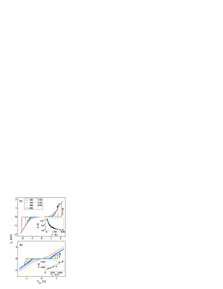
Figure 1a shows characteristics of a nanocrystal device at selected temperatures. When cooling, zero-bias conductance decreases monotonically until . Below , the characteristics show sharp switching between a low bias insulating state and a high bias state with much higher differential conductance (close to , with dramatic hysteresis as a function of voltage sweep direction. The switching threshold voltages increase in magnitude as is decreased.
Dozens of nanocrystal devices were measured and only those with 300 K resistances below 10 k showed the switching, with higher resistance devices having higher switching threshold voltages. Resistances decrease by some three orders of magnitude with vacuum annealing at 673 K, likely because of oleic acid decomposition.Perezdieste:2003 ; Zeng:2006 The temperature dependence (Fig. 1a, inset) of the zero-bias resistance, , has no step at , showing that remains dominated by contact effects.
Qualitatively identical conduction is apparent in the thin film devices, as shown in Fig. 1b. Contact resistances are also important in these structures, as demonstrated by examining at low bias ( mV) as a function of channel length, , as shown in the inset for one set of devices. Extrapolating back to , the contact resistance, , at 300 K is 390 , while the 50 nm thick channel of width 20 m contributes 27.2 /micron, implying (based on channel geometry) a magnetite resistivity of 2.9 m-cm, somewhat below bulk expectations. Further investigations are seeking to understand and minimize . Analysis of at lower temperatures shows that increases significantly as is decreased, exceeding 80 k by 80 K. This complicates the analysis of the switching, since some of the total is dropped across rather than directly within the Fe3O4; further, the contacts may not be Ohmic near the switching threshold. We return to this issue later.
The transitions in all devices are extremely sharp, with widths less than 50 V, though in repeated sweeps at a fixed temperature, there is sweep-to-sweep variability of a few mV in switching thresholds. Using the substrate as a gate electrode, no discernable gate modulation was seen in nanocrystal devices for gate biases between -80 V and +80 V; this suggests that nanocrystal charging effects do not dominate. Switching characteristics were independent of magnetic field perpendicular to the sample surface up to 9 T, showing no large coupling between magnetization and the transition.
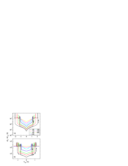
Differential conductance traces (Figure 2) show the transition even more dramatically. In the high conductance state, is relatively temperature independent. As is decreased, a clear zero-bias suppression develops, deepening into a hard gap when . In the nanocrystal data there are indications (in ) of gap formation even at 150 K. We note that in nanocrystals could be elevated, since nanocrystals have large surface-to-volume ratios and the transition temperature of the magnetite surface is known to be higher than in the bulk.Shvets:2004

Several lines of evidence indicate that these sharp conductance transitions are not the result of local Joule heating (as in macroscopic samples of Fe3O4 Burch:1969 ; Freud:1969 and in the Mott insulator VO2 Duchene:1971 ; Gu:2007 ), but rather are electrically driven. In the worst-case scenario, all of the Joule heating power is dissipated within the magnetite, and inhomogeneous dissipation (e.g., filamentary conduction through a locally heated path) can complicate the analysis. The local steady-state temperature is determined by the power dissipated and the thermal path. Thermally driven switching would then correspond to raising the local temperature above . At a fixed cryostat temperature an improved thermal path would imply that more power dissipation would be required for a given local temperature rise. Similarly, for a fixed thermal path, the necessary dissipated power for thermal switching would approach zero as . Furthermore, at a given cryostat temperature thermally-driven switching would imply that the power dissipated at the low-to-high conductance transition (needed to raise the local temperature to ) should be close to that at the high-to-low conductance transition.
The thermal conductivity, , of magnetite is dominated by phonons in this temperature range, and limited by phonon-electron scattering,Salazar:2004 even when . As a result, increases as is decreased through and below , and the material’s thermal coupling to the cryostat improves as is reduced. In all devices showing switching, the electrical power required to switch from low to high conductance decreases with decreasing , with Fig. 3 showing one example. This is precisely the opposite of what one would expect from thermally-driven switching. Similarly, in all devices the power dissipated at switching does not approach zero as , again inconsistent with thermally-driven switching. Furthermore, at a given the power dissipated just before is swept back down through the high-to-low conductance threshold significantly exceeds that dissipated at the low-to-high point in many devices, including those in Fig. 1, inconsistent with thermal switching expectations. Finally, nanocrystal and thin film devices show quantitatively similar switching properties and trends with temperature, despite what would be expected to be very different thermal paths. These switching characteristics are also qualitatively very different from those in known inhomogeneous Joule heating.Burch:1969 ; Freud:1969 . These facts rule out local heating through the Verwey transition as the cause of the conductance switching.
Figure 3 (inset) shows details of hysteresis loops on a nanocrystal device comparing different voltage sweep rates. The loop shape and switching voltages are unchanged to within the precision of the data collection as voltage sweep rates are varied from around 0.7 V/s up to 70 V/s. This indicates that the switching process is relatively rapid. Further studies will examine the intrinsic switching speed.
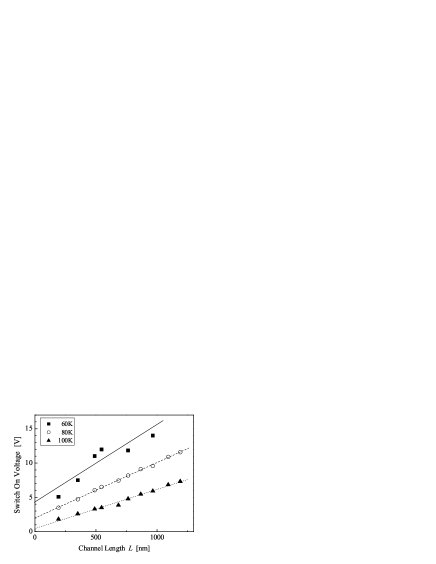
The observed conductance transition appears to be driven electrically. Figure 4 is a plot of the low-to-high conductance switching voltage as a function of in a series of film devices for several temperatures. The linear dependence implies that the transition is driven by electric field itself, rather than by the absolute magnitude of the voltage or the current density. The fact that the voltage extrapolates to a nonzero value at is likely a contact resistance effect. Minimizing and better understanding the contact resistance will allow the determination of the electric field distribution within the channel.
The length scaling of the transition voltage also demonstrates that this is a bulk effect. The contacts in all of these devices are identical, so any change in switching properties must result from the magnetite channel. This is in contrast to the resistive switching in Pr0.7Ca0.3MnO3 (PCMO) that is ascribed to a change in contact resistance due to occupation of interfacial statesSawa:2004 .
The field-driven conductance transition may give insights into the equilibrium Verwey transition. This switching may be useful in testing recent calculationsPiekarz:2006 ; Leonov:2006 ; Pinto:2006 about the role of strongly correlated B-site Fe 3 electrons and their coupling to phonons in the Verwey transition mechanism. It is interesting to ask, to what degree is the field-driven electronic transition coupled to the local structure? It is greatly desirable to perform local probes of the magnetite structure (via x-ray or electron-diffraction techniques or scanned probe microscopy) in situ in the channel of biased devices, to see if the coherence between structural symmetry changes and the formation of a gap in the electronic spectrum is broken under these noequilibrium conditions. This is a significant experimental challenge. Similarly, local Raman spectroscopy of devices under bias could reveal field-induced changes in phonon modes and electron-phonon couplings, and single-crystal thin films permit the application of bias along well-defined crystallographic directions relevant to structural symmetry changes at . We do note that qualitatively identical switching occurs in nanocrystal devices as in strained thin films strongly coupled to rigid MgO substrates. This suggests that elastic constraints on scales much larger than the unit cell have relatively little influence on the observed switching.
It is also possible that the nonequilibrium carrier distribution contributes to destabilizing the insulating state. In the presence of a strong electric field a carrier can gain significant energy even in a single hopping step, even though carrier relaxation times are very short. A rough estimate of the average critical -field for switching at 80 K is V/m, from the slope of the line in Fig. 4. The high temperature cubic unit cell is 0.84 nm on a side, meaning that a carrier traversing one cell would gain approximately 8.4 meV, comparable to 10.3 meV. Conductance switching at such high fields may require consideration of such nonequilibrium carrier dynamics.
The presence of multiple switching transitions in individual nanocrystal and film devices also bears further study. The suggested charge order may melt inhomogeneously, with portions of the channel having different switching thresholds. There could also be charge-ordered intermediate states between the insulating regime and the most conducting regime.Walz:2002 Again, optical measurementsGasparov:2000 with sufficient spatial resolution could address these possibilities. Through improved metal/magnetite contacts and further study, it should be possible to unravel the precise nature of this nonequilibrium transition, and its relationship to the equilibrium, bulk Verwey transition.
I Methods
Magnetite nanocrystals were prepared via solution-phase decomposition of iron carboxylate salts.Yu:2004 The nanocrystals have been characterized by transmission electron microscopy (TEM), x-ray diffraction, and infrared and Raman spectroscopy, as discussed in Supplemental Material. As synthesized the nanocrystals are protected by weakly bound oleic acid ligands; these ligands allow the suspension of the nanocrystals in organic solvents, but act as electrically insulating layers that must be largely removed for effective electronic transport measurements.
Two-step electron beam lithography and e-beam evaporation (1 nm Ti, 15 nm Au) were used to pattern closely spaced source and drain electrode pairs onto degenerately -doped silicon substrates coated with 200 nm of thermally grown SiO2. Interelectrode gaps (channel lengths) ranged from zero to tens of nm, with a 10 m wide channel region. Nanocrystals were spin-coated from hexane solutions to form slightly more than one densely packed monolayer of nanocrystals over the channel region. Samples were then baked at 673 K in vacuum for 1 hr to remove as much of the oleic acid as possible. In one set of samples, a second layer of particles was added followed by a second round of baking.
The other class of devices are based on epitaxial magnetite films 50 nm thick grown by oxygen-plasma-assisted molecular beam epitaxy (MBE) on MgO single-crystal substrates. Details of the growth process have been reported elsewhere.Zhou:2004 Single-step e-beam lithography and e-beam evaporation were used to pattern Au (no Ti adhesion layer) source and drain electrodes defining a channel length ranging from tens of nm to hundreds of nm, and a channel width of 20 m. The interelectrode conduction is dominated by the channel region due to this geometry. No annealing was performed following electrode deposition.
References
- (1) Mills, A. A. The lodestone: history, physics, and formation. Ann. Science 61, 273-319 (2004).
- (2) Coey, J. M. D. & Chien, C. L. Half-metallic ferromagnetic oxides. MRS Bulletin 28, 720-724 (2003).
- (3) Verwey, E. J. W. Electronic conduction in magnetite (Fe3O4) and its transition point at low temperatures. Nature 144, 327-328 (1939).
- (4) Verwey, E. J. W. & Haayman, P. W. Electronic conductivity and transition point of magnetite. Physica 8, 979-987 (1941).
- (5) Walz, F. The Verwey transition - a topical review. J. Phys.: Condens. Matter 14, R285-R340 (2002).
- (6) Garciá, J. & Subías, G. The Verwey transition - a new perspective. J. Phys.:Condens. Matter 16, R145-R178 (2004).
- (7) Huang, D. L. et al. Charge-orbital ordering and Verwey transition in magnetite measured by resonant soft x-ray scattering. Phys. Rev. Lett. 96, 096401 (2006).
- (8) Nazarenko, E. et al. Resonant x-ray diffraction studies on the charge ordering in magnetite. Phys. Rev. Lett. 97, 056403 (2007).
- (9) Subías, G. et al. Magnetite, a model system for mixed-valence oxides, does not show charge ordering. Phys. Rev. Lett. 93, 156408 (2004).
- (10) Rozenberg, G. K. et al. Origin of the Verwey transition in magnetite. Phys. Rev. Lett. 96, 045705 (2006).
- (11) Piekarz, P., Parlinksi, K. & Oleś, A. M. Mechanism of the Verwey transition in magnetite. Phys. Rev. Lett. 97, 156402 (2006).
- (12) Gasparov, L. V. et al. Infrared and Raman studies of the Verwey transition in magnetite. Phys. Rev. B 62, 7939-7944 (2000).
- (13) Imada, M., Fujimori, A. & Tokura, Y. Metal-insulator transitions. Rev. Mod. Phys. 70, 1039-1263 (1998).
- (14) Coey, M. Condensed-matter physics: Charge-ordering in oxides. Nature 430, 155-157 (2004).
- (15) Leonov, I., Yaresko, A. N., Antonov, V. N. & Anisimov, V. I. Electronic structure of charge-ordered Fe3O4 from calculated optical, magneto-optical Kerr effect, and O -edge x-ray absorption spectra. Phys. Rev. B 74, 165117 (2006).
- (16) Pinto, H. P. & Elliot, S. D. Mechanism of the Verwey transition in magnetite: Jahn-Teller distortion and charge ordering patterns. J. Phys.: Condens. Matter 18, 10427-10436 (2006).
- (17) Asamitsu, A., Tomioka, Y., Kuwahara, H. & Tokura, Y. Current switching of ressitive states in magnetoresistive manganites. Nature 388, 50-52 (1997).
- (18) Sawa, A., Fujii, T., Kawasaki, M. & Tokura, Y. Hysteretic current-voltage characteristics and resistance switching at a rectifying Ti/Pr0.7Ca0.3MnO3 interface. Appl. Phys. Lett. 85, 4073-4075 (2004).
- (19) Yu, W. W., Falkner, J. C., Yavuz, C. T. & Colvin, V. L. Synthesis of monodisperse iron oxide nanocrystals by thermal decomposition of iron carboxylate salts. Chem. Commun. 2004, 2306-2307 (2004).
- (20) Zhou, Y., Jin, X. & Shvets, I. V. Enhancement of the magnetization saturation in magnetite (100) epitaxial films by thermo-chemical treatment. J. Appl. Phys. 95, 7357-7359 (2004).
- (21) Pérez-Diete, V. et al. Thermal decomposition of surfactant coatings on Co and Ni nanocrystals. Appl. Phys. Lett. 83, 5053-5055 (2003).
- (22) Zeng, H. et al. Magnetotransport of magnetite nanoparticle arrays. Phys. Rev. B 73, 020402(R) (2006).
- (23) Shvets, I. V. et al. Long-range charge order on the Fe3O4(001) surface. Phys. Rev. B 70, 155406 (2004).
- (24) Burch, T. et al. Switching in magnetite: a thermally driven magnetic phase transition. Phys. Rev. Lett. 23, 1444-1447 (1969).
- (25) Freud, P. J. & Hed, A. Z. Dynamics of the electric-field-induced conductivity transition in magnetite. Phys. Rev. Lett. 23, 1440-1443 (1969).
- (26) Duchene, J., Terraillon, M., Pailly, P. & Adam, G. Filamentary conduction in VO2 coplanar thin-film devices. Appl. Phys. Lett. 19, 115-117 (1971).
- (27) Gu, Q., Falk, A., Wu, J., Ouyang, L. & Park, H. Current-driven phase oscillation and domain-wall propagation in WxV1-xO2 nanobeams. Nano Lett. 7, 363-366 (2007).
- (28) Salazar, A., Oleaga, A., Wiechec, A., Tarnawski, Z. & Kozlowski, A. Thermal diffusivity of Fe3-xZnxO4. IEEE Trans. Magn. 40, 2820-2822 (2007).
II Addendum
Supplementary Information is linked to the online version of the paper.
Acknowledgements. This work was supported by the US Department
of Energy grant DE-FG02-06ER46337. DN also acknowledges the David
and Lucille Packard Foundation and the Research Corporation. VLC
acknowledges the NSF Center for Biological and Environmental
Nanotechnology (EEC-0647452), Office of Naval Research
(N00014-04-1-0003), and the US Environmental Protection Agency Star
Program (RD-83253601-0). CTY acknowledges a Robert A. Welch
Foundation (C-1349) graduate fellowship. RGSS and IVS acknowledge
the Science Foundation Ireland grant 06/IN.1/I91.
Author Contributions. SL fabricated and measured the devices in this work and analyzed the data. AF fabricated devices and performed XRD characterization of the nanocrystal materials. DN and SL wrote the paper. JTM and CYZ made the nanocrystals in VLC’s laboratory, and VLC contributed expertise in nanomaterials chemistry and characterization. RGSS and IVS grew the magnetite films, and IVS contributed expertise on magnetite physical properties. All authors discussed the results and commented on the manuscript.
Competing Interests. The authors declare that they have no competing financial interests.
Correspondence. Correspondence and requests for materials should be addressed to D.N. (email: natelson@rice.edu).