ELECTRICAL CONTROL OF SURFACE–WAVE PROPAGATION AT THE PLANAR INTERFACE OF A LINEAR ELECTRO–OPTIC MATERIAL AND AN ISOTROPIC DIELECTRIC MATERIAL
SUDARSHAN R. NELATURY
Department of Electrical, Computer and Software Engineering,
Pennsylvania State University, The Behrend College,
5101 Jordan Road, Erie, PA 16563-1701, USA.
JOHN A. POLO JR.
Department of Physics and Technology,
Edinboro University of Pennyslvania,
235 Scotland Rd., Edinboro, PA 16444, USA.
AKHLESH LAKHTAKIA
CATMAS — Computational & Theoretical Materials Sciences Group,
Department of Engineering Science and
Mechanics,
Pennsylvania State University, University Park, PA 16802, USA.
Abstract
Surface waves can propagate on the planar interface of a linear electro-optic (EO) material and an isotropic dielectric material, for restricted ranges of the orientation angles of the EO material and the refractive index of the isotropic material. These ranges can be controlled by the application of a dc electric field, and depend on both the magnitude and the direction of the dc field. Thus, surface-wave propagation can be electrically controlled by exploiting the Pockels effect.
Key words: Electro-optics, Pockels effect, surface wave
1 Introduction
Wave propagation localized to a planar metal-dielectric interface has a long history (Zenneck, 1907; Agranovich and Mills, 1982; Boardman, 1982; Homola et al., 1999; Matveeva et al., 2005). In contrast, wave propagation localized to the planar interface of an isotropic dielectric material and a uniaxial dielectric material was found possible by D’yakonov only in 1988 (D’yakonov, 1988; Averkiev and Dyakonov, 1990). Since then, researchers have explored surface-wave propagation (SWP) on increasingly complex systems of bimaterial interfaces such as biaxial-isotropic, uniaxial-uniaxial, and biaxial-biaxial (Walker et al., 1998; Darinskiĭ 2001, Wong et al., 2005; Polo et al., 2006, 2007a,b; Nelatury et al., 2007). In all such investigations, essentially, one looks for the selected angular regimes of the propagation direction wherein certain dispersion conditions are met. For complex systems, the angular regimes are very narrow and depend highly on the crystallographic symmetries of the two materials.
Our motivation for this paper is to show how one might exercise control on the angular regimes of SWP. Whereas temperature and pressure may be altered to control SWP, the application of an external field is expected to provide dynamic control. In particular, the electro-optic effect refers to changes in optical properties by the application of a low-frequency or dc electric field. For instance, an optically isotropic crystal (possessing either the or point group symmetry) upon exposure to a dc electric field turns birefringent (Cook, 1996; Lakhtakia, 2006a).
The Pockels effect is a linear electro-optic (EO) effect, whereby the modification of the inverse (optical) permittivity matrix by the dc electric field is quantified through 18 electro-optic coefficients, not all of which may be independent of each other, depending on the point group symmetry (Boyd, 1992). The opportunities offered by the Pockels effect for tuning the optical response characteristics of materials have recently been highlighted for photonic band-gap engineering (Lakhtakia, 2006b; Li et al., 2007) and composite materials (Lakhtakia and Mackay, 2007; Mackay and Lakhtakia, 2007). These publications suggest that, although the changes in the optical permittivity matrix are typically small, the effect on SWP could be significant due to the extreme sensitivity of surface waves on the dielectric constitutive properties. Let us note here an earlier study wherein the quadratic EO effect named after Kerr was shown to offer control over SWP (Torner et al., 1993).
This paper introduces the influence of the Pockels effect on SWP. Although the theoretical treatment is general, numerical results are presented only for a specific EO material: potassium niobate (Zgonik et al., 1993). The remainder of the paper is organized as follows: Section 2 provides a description of a canonical boundary-value problem, the optical permittivity matrix of an EO crystal, and the derivation of the dispersion relations for SWP. In Section 3 numerical results are furnished, and our conclusions are distilled in Section 4. A note on notation: vectors are underlined, matrixes are decorated with an overbar, and the Cartesian unit vectors are denoted as , , and . All field quantities are assumed to have an time-dependence.
2 Theory
Let the plane of SWP be a bimaterial interface. The half-space is filled with a homogeneous, isotropic, dielectric material with an optical refractive index denoted by . The half-space is filled with a homogeneous, linear, EO material, whose optical relative permittivity matrix is stated as (Lakhtakia and Reyes 2006a,b)
| (1) |
Incorporating the Pockels effect due to an arbitrarily oriented but uniform dc electric field , the matrix is given by
| (2) |
correct to the first order in , where
| (3) |
are the principal relative permittivity scalars in the optical regime, whereas (with and ) are the EO coefficients. The EO material can be isotropic, uniaxial, or biaxial, depending on the relative values of , , and . Furthermore, the EO material may belong to one of 20 crystallographic classes of point group symmetry, in accordance with the relative values of the EO coefficients .
The rotation matrix
| (4) |
in Equation (1) denotes a rotation about the axis by an angle . The matrix
| (5) |
involves the angle with respect to the axis in the plane, and combines a rotation as well as an inversion. The angles and delineate the orientation of the EO material in the laboratory coordinate system, the full transformation from laboratory coordinates () to those used conventionally for EO materials () being illustrated in Figure 1.
 |
Now is a symmetric matrix, regardless of the magnitude and direction of . With the assumption that all of its elements are real-valued, can be written as , where and are scalars and the unit vectors and are parallel to the crystallographic axes or the optical ray axes of the EO material in the () coordinate system (Chen 1983). Likewise, can be written as , where and are scalars and the unit vectors and are parallel to the optic axes of the EO material in the () coordinate system. Thus, the application of the uniform dc electric field not only changes the eigenvalues of , but also rotates both optic axes and both optical ray axes, in general.
2.1 Field representations
Without loss of generality we assume that the SWP direction is parallel to the axis. The fields in the half-space must satisfy the equations
| (6) |
where and are the permittivity and permeability of free space, and and are the complex-valued amplitudes of the electric and magnetic field phasors in the isotropic dielectric material. The wave vector
| (7) |
where and
| (8) |
are the normalized propagation constant and the decay constant, respectively, whereas is the free-space wavenumber. We must have for SWP; furthermore, must be real-valued and positive for un-attenuated propagation along the axis. Accordingly, the acceptable solutions of Equations (6) are
| (9) |
and
| (10) |
where and are unknown scalars. If is purely real-valued, the electric and magnetic field phasors of the surface wave decay exponentially with respect to as ; otherwise, the decay is damped sinusoidal.
The fields in the half-space must be solutions of the equations
| (11) |
The wave vector
| (12) |
must have for localization of energy to the bimaterial interface. A purely real-valued indicates an exponential decay of the field phasors with respect to as , whereas indicates a damped-sinusoidal decay.
Substitution of into Equations (11) yields a set of six homogenous equations that are linear in the six Cartesian components of and . Setting the determinant of the coefficients equal to zero gives the dispersion equation
| (13) |
where the coefficients
| (14) | |||||
| (15) | |||||
| (16) | |||||
| (17) | |||||
| (18) |
involve , etc.
The solution of Equation (13) leads to four values of . We select the two values of that conform to the restriction , and label them as and . The corresponding wave vectors in the EO material are denoted by and . Accordingly, with unknown coefficients and , we write the Cartesian components of the field phasors in the half-space as
| (19) | |||||
| (20) | |||||
| (21) | |||||
| (22) | |||||
| (26) | |||||
| (27) |
2.2 Boundary conditions
The boundary conditions at the interface lead to the following four equations:
| (28) |
These equations may be cast in matrix form as
| (29) |
where is a 44 matrix. For a non-trivial solution, the determinant of must equal zero; thus, the SWP dispersion equation is
| (30) |
Because of the complexity of Equation (30), an algebraic result could not be obtained and recourse was taken to a numerical method of solution. Parenthetically, when , the Pockels effect is not invoked, and the presented formulation simplifies to that of Polo et al. (2007a).
3 Numerical Results and Discussion
The Pockels effect occurs only in dielectric materials that lack inversion symmetry. Some examples of materials of this type are potassium niobate, lithium niobate and gallium arsenide. We chose potassium niobate for calculations since it has very large EO coefficients. As potassium niobate belongs to the orthorhombic class, the only non-zero EO coefficients are , , , , and ; hence, we get
| (31) |
from Equation (2). Constitutive data for potassium niobate are as follows (Zgonik et al., 1993): , , , m V-1, m V-1, m V-1, m V-1, and m V-1.
The existence of a surface wave was determined at various values of , , and by satisfactory solution of Equation (28). Purely for illustrative purposes, the most detailed calculations were performed at only one value of : ; at this value of the range of propagation directions is relatively wide. Let us note that the range of values of for SWP at the planar interface of a non-EO biaxial dielectric material and a non-EO isotropic material is limited (Polo et al., 2007), and the range of values of the orientation angle for a specific is quite small as well. In the remainder of this section, the mid-point of the -range is denoted by and the width of that range by .
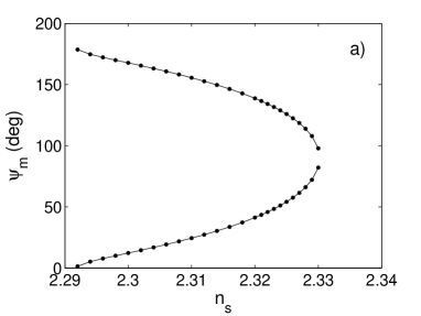
3.1 Results for
In order to provide a baseline for the influence of the Pockels effect on SWP, Figure 2 shows and as functions of for when . The plots in the figure cover the entire -range over which SWP was found possible. The -range extends from approximately to , and is thus only in width. The -range in the figure is limited to ; if SWP is possible for a certain value of , it is also possible for , when .
Over the range two bands of values for SWP can be deduced from Figure 2 for each value of , except at the largest value of where the two bands coalesce. At the lower limit of the -range, approaches either or ; while at the upper limit of that range, approaches for both bands. When one considers the entire -range (i.e., ), there are four bands of -values that merge into two bands at both limits of the -range.
|
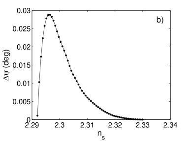
In Figure 2b, is shown as a function of . Only one curve is shown since both -bands have the same width at each value of . The curve has a single peak and goes to zero at the two endpoints of the -range. The maximum value of is about and occurs at , i.e., near the lower endpoint of the -range. Thus, the –bands for SWP are really narrow.
In order to explore the influence of the Pockels effect on SWP, was next set equal to V m-1. This dc field was oriented along each of the laboratory coordinate axes and ) separately. We now describe the results for each direction of orientation of the dc electric field in order of increasing complexity.
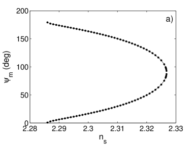
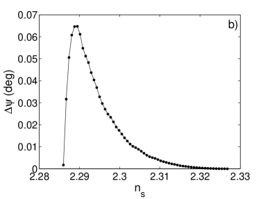
Let us begin with V m-1. Both and are plotted against in Figure 3. Just as for the plots for already discussed, there are four -bands with mirror symmetry about the -axis. Figure 3a shows that the -range for SWP has grown slightly and shifted to lower values of compared to Figure 2a. With approximate lower and upper endpoints of 2.286 and 2.327 respectively, the width of the -range is 0.041. Both -bands meet at , which is just the same as in the absence of the dc electric field. In Figure 3b, a single curve describes the widths of both -bands as varies, which is similar to the curve in Figure 2b for . The height of the -peak, however, is approximately , a little more than double that of the peak for , and occurs at .
|
Figure 4 shows the - and - curves when V m-1. Just as in the previous two cases, there are four -bands with mirror symmetry about the -axis. So, only two -bands are shown in the figure. Evidently from Figure 4a, the -range for SWP is larger than when the dc electric field is either absent or aligned parallel to the axis. The width of the -range for SWP has grown to 0.049, with the lower and upper endpoints of the -range being 2.289 and 2.338, respectively. Although both -bands in Figure 4a have wider -ranges than in the previous two figures, the upper band (labeled Band 2), has increased more than the lower band (Band 1). In addition, the two -bands meet at a lower value of (), and, thus, lack the symmetry about seen in Figures 2a and 3a for the cases of and , respectively.
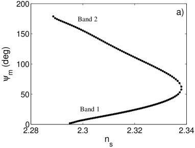
|
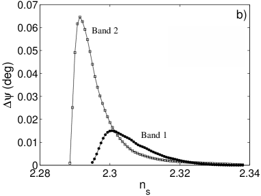
Both -bands in Figure 4b still show a single -peak each, towards the lower endpoint of the -range. However, the - curves for the two bands are not identical. Whereas the -peak for Band 2 is about the same as for in Figure 3b, the -peak for Band 1 is about a third of that value. In addition, the positions of the -peaks are shifted slightly from the value for , with the peak for Band 2 shifted downward to and that for Band 1 upward to .
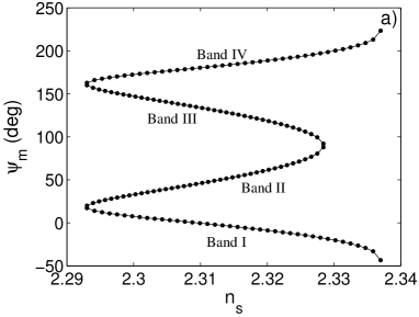
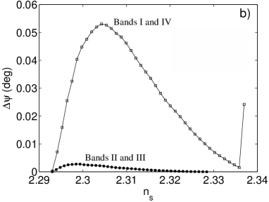
Figure 5 displays the influence of the dc electric field when applied along the axis, i.e., V m-1. In Figure 5a, the full range of , , is displayed as the -bands for SWP are no longer symmetric about ; instead, these bands (labeled I to IV) are now located symmetrically about . The widths of the -bands are shown in Figure 5b. As is the case for the dc electric field applied parallel to the axis, the widths of all four bands are not equal. Band I with a -range of approximately and Band IV with an approximate -range of have the same width as a function of . The maximum width of these two -bands is about and occurs near . Similarly, Band II with a -range of and Band III with a -range of share a common - curve. The widths of Bands II and III are more than a factor of 10 smaller than of Bands I and IV, the -peak for Bands II and III being at .
|
The sudden change in at the upper endpoint of the range for Bands I and IV in Figure 5b should be noted. A similar sudden change was also found for . The region of coalescence of two bands on the -axis is hard to delineate accurately. Quite possibly, the sudden change is a numerical artifact; it will be the subject of future investigations.
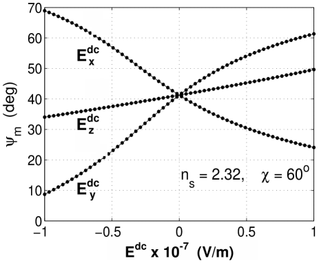
The effect of variation of the magnitude of the dc electric field is shown in Figure 6 with a plot of vs. the dc field’s signed magnitude, for parallel to the , , and axes. For the dc field oriented along both the and the axes, increases as the signed magnitude becomes more positive: the relationship is nearly linear for , and somewhat S-shaped for . On the other hand, when , decreases as the signed magnitude becomes more positive. The foregoing results clearly show that by varying the magnitude and/or direction of the dc electric field, the direction of SWP, relative to the crystal axes of the EO material, can be controlled.
 |
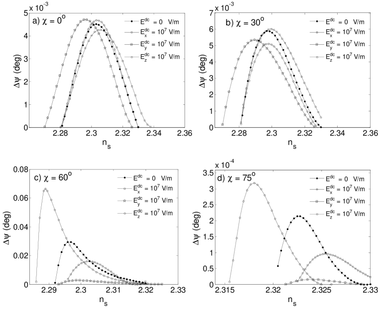
3.2 Results for other
Limited results were also obtained for , , and , with the search for SWP restricted to . Figure 7 contains - curves for , for (a) and (b) of signed magnitude V m-1 and parallel to the , , and axes. Although both Band 1 and Band 2 (when ) and Band I and Band II (when ) should be visible in the plots, for simplicity, only Band 1 and Band II are shown.
The curves for the chosen values of are isomorphic. At each value of , a marked downward shift of the - curve, compared to the case for , occurs when , and an upward shift for . There is also a shift for , but it is much smaller and is almost unnoticeable at the lower values of ; however, the shift is significant for , on the same order as when the dc electric field is applied along the other two axes.
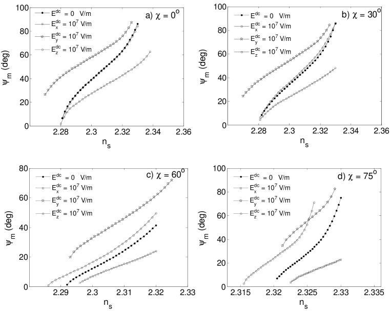
Figure 8 shows - curves for , for the dc electric field configured as for Figure 7. When , the curves for all three orientations of the dc field and the zero dc field are similar, having nearly the same peak values of and peaking at close to the same values of . As increases, the curves become differentiated both in the peak height and its position on the axis. Among the four values of explored, the largest peak values of occur for . This is particularly true when ; then some values of are more than an order of magnitude larger than found at other values of .
4 Concluding remarks
The influence of the Pockels effect on SWP at the interface between potassium niobate and an isotropic dielectric material has been demonstrated by our numerical studies. With the application of a dc electric field, we have noted the shift in the -range and the -bands that permit SWP. The greatest influence of the Pockels effect is on the median propagation angle of the very narrow -bands in which SWP is possible. Shifts of over at a fixed value of have been deduced. Thus, the Pockels effect can be pressed into service for an electrically controlled on-off switch for surface waves.
As of now, the existence of surface waves at the planar interface between a biaxial dielectric material and an isotropic dieletric material has not been demonstrated experimentally. The narrow - and -regimes for SWP may discourage experimentalists from searching for surface waves in these scenarios. Electrical control of SWP direction may provide a convenient way to search for surface waves. The experiment could be carried out with a fixed geometry defining the propagation direction and the orientation of the linear EO material, and the signed magnitude of could then easily be swept electronically until a surface wave is detected. Various experimental configurations for exciting surface waves are available (Agranovich and Mills, 1982), as also are optically transparent electrodes to apply dc electric fields (Minami 2005; Medvedeva 2007). Finally, we hope that our work shall spur the development of artificial linear EO materials with much higher EO coefficients than now available.
References
-
Agranovich, V. M., & D. L. Mills. (Eds.) 1982. Surface Polaritons: Electromagnetic Waves at Surfaces and Interfaces. Amsterdam: North-Holland.
-
Averkiev, N. S., & M. I. Dyakonov. 1990. Electromagnetic waves localized at the interface of transparent anisotropic media. Opt. Spectrosc. (USSR) 68:653-655.
-
Boardman, A. D. (Ed.) 1982. Electromagnetic Surface Modes. Chichester: Wiley.
-
Boyd, R. W. 1992. Nonlinear Optics. San Diego: Academic.
-
Chen, H. C. 1983. Theory of Electromagnetic Waves: A Coordinate-Free Approach, 219-226. New York: McGraw-Hill.
-
Cook, Jr., W. C. 1996. Electrooptic coefficients. In: Nelson, D.F. (Ed.) 1996. Landolt-Bornstein, Vol. 3/30A, 164. Berlin: Springer.
-
Darinskiĭ, A. N. 2001. Dispersionless polaritons on a twist boundary in optically uniaxial crystals. Crystallogr. Repts. 46:842-844.
-
D’yakonov, M. I. 1988. New type of electromagnetic wave propagating at an interface. Sov. Phys. JETP 67:714-716.
-
Farias, G. A., E. F. Nobre, & R. Moretzsohn. 2002. Polaritons in hollow cylinders in the presence of a dc magnetic field. J. Opt. Soc. Am. A 19:2449-2455.
-
Homola, J., S. S. Yee, & G. Gauglitz. 1999. Surface plasmon resonance sensors: review. Sens. Actuat. B: Chem. 54:3-15.
-
Lakhtakia, A. 2006a. Electrically switchable exhibition of circular Bragg phenomenon by an isotropic slab. Microw. Opt. Technol. Lett. 48:2148-2153; corrections: 2007. 49:250-251.
-
Lakhtakia, A. 2006b. Narrowband and ultranarrowband filters with electro-optic structurally chiral materials. Asian J. Phys. 15:275-282.
-
Lakhtakia, A., & T. G. Mackay. 2007. Electrical control of the linear optical properties of particulate composite materials. Proc. R. Soc. Lond. A 463:583-592.
-
Lakhtakia, A., & J. A. Reyes. 2006a. Theory of electrically controlled exhibition of circular Bragg phenomenon by an obliquely excited structurally chiral material – Part 1: Axial dc electric field. Optik doi:10.1016/j.ijleo.2006.12.001.
-
Lakhtakia, A., & J. A. Reyes. 2006b. Theory of electrically controlled exhibition of circular Bragg phenomenon by an obliquely excited structurally chiral material – Part 2: Arbitrary dc electric field. Optik doi:10.1016/j.ijleo.2006.12.002.
-
Li, J., M.-H. Lu, L. Feng, X.-P. Liu, & Y.-F. Chen. 2007. Tunable negative refraction based on the Pockels effect in two-dimensional photonic crystals composed of electro-optic crystals. J. Appl. Phys. 101:013516.
-
Mackay, T. G., & A. Lakhtakia. 2007. Scattering loss in electro-optic particulate composite materials. J. Appl. Phys. 101:083523.
-
Matveeva, E., Z. Gryczynski, J. Malicka, J. Lukomska, S. Makowiec, K. Berndt, J. Lakowicz, & I. Gryczynski. 2005. Directional surface plasmon-coupled emission: Application for an immunoassay in whole blood. Anal. Biochem. 344:161-167.
-
Medvedeva, J. E. 2007. Unconventional approaches to combine optical transparency with electrical conductivity. Appl. Phys. A doi:10.1007/s00339-007-4035-4.
-
Minami, T. 2005. Transparent conducting oxide semiconductors for transparent electrodes. Semicond. Sci. Technol. 20:S35-S44.
-
Mineralogy Database, http://www.webmineral.com/ (20 April 2006).
-
Nelatury, S. R., J. A. Polo Jr., & A. Lakhtakia. 2007. Surface waves with simple exponential transverse decay at a biaxial bicrystalline interface. J. Opt. Soc. Am. A 24:856-865; corrections: 24:2102.
-
Polo Jr., J. A., S. Nelatury, & A. Lakhtakia. 2006. Surface electromagnetic wave at a tilted uniaxial bicrystalline interface. Electromagnetics 26:629-642.
-
Polo Jr., J. A., S. R. Nelatury, & A. Lakhtakia. 2007a. Propagation of surface waves at the planar interface of a columnar thin film and an isotropic substrate. J. Nanophoton. 1, 013501.
-
Polo Jr., J. A., S. R. Nelatury, & A. Lakhtakia. 2007b. Surface waves at a biaxial bicrystalline interface. J. Opt. Soc. Am. A 24:xxxx-xxxx (at press).
-
Torner, L., J. P. Torres, F. Lederer, D. Mihalache, D. M. Baboiu, & M. Ciumac. 1993. Nonlinear hybrid waves guided by birefringent interfaces. Electron. Lett. 29:1186-1188.
-
Torreri, P., M. Ceccarini, P. Macioce, & T. Petrucci. 2005. Biomolecular interactions by surface plasmon resonance technology. Ann. Ist. Super. Sanità 41:437-441.
-
Walker, D. B., E. N. Glytsis, & T. K. Gaylord. 1998. Surface mode at isotropic-uniaxial and isotropic-biaxial interfaces. J. Opt. Soc. Am. A 15:248-260.
-
Wong, C., H. Ho, K. Chan, S. Wu, & C. Lin. 2005. Application of spectral surface plasmon resonance to gas pressure sensing. Opt. Eng. 44:124403.
-
Zenneck, J. 1907. Über die Fortpflanzung ebener elektromagnetischer Wellen längs einer ebenen Lieterfläche und ihre Beziehung zur drahtlosen Telegraphie. Ann. Phys. Lpz. 23:846-866.
-
Zgonik, M., R. Schlesser, I. Biaggio, E. Volt, J. Tscherry, & P. Günter. 1993. Material constants of KNbO3 relevant for electro- and acousto-optics. J. Appl. Phys. 74:1287-1297.