Experimental Test of the Dynamical Coulomb Blockade Theory for Short Coherent Conductors
Abstract
We observed the recently predicted quantum suppression of dynamical Coulomb blockade on short coherent conductors by measuring the conductance of a quantum point contact embedded in a tunable on-chip circuit. Taking advantage of the circuit modularity we measured most parameters used by the theory. This allowed us to perform a reliable and quantitative experimental test of the theory. Dynamical Coulomb blockade corrections, probed up to the second conductance plateau of the quantum point contact, are found to be accurately normalized by the same Fano factor as quantum shot noise, in excellent agreement with the theoretical predictions.
pacs:
73.23.-b, 73.23.Hk, 72.70.+mA tunnel junction exhibits a drop of its conductance at low voltages and temperatures when it is embedded in a resistive circuit, in violation of the classical impedances composition laws. This quantum phenomenon, known as dynamical Coulomb blockade (DCB), results from the excitation of the circuit’s electromagnetic modes by the current pulses associated with tunnel events. The theory is well understood and verified experimentally for tunnel junctions SCT ; DEVetal1990_GIRVINetal1990 ; CLELANDetal1992_HOLSTetal1994 ; JOYEZetal1998 ; PIERREetal2001 , but it is only recently that it has been extended to short coherent conductors GZ2001_LEVYYEYATIetal2001 . The strong recent prediction is that DCB corrections are simply reduced by the same normalization factor as quantum shot noise, as a consequence of electron flow regulation by the Pauli exclusion principle MARTINLANDAUER1992 . The aim of this work is to perform an accurate experimental test of the DCB theory for coherent conductors and thereby to provide solid grounds to our knowledge of impedances composition laws in mesoscopic circuits.
A powerful description of coherent conductors in absence of interactions is provided by the scattering approach, which encapsulates the complexity of transport mechanisms into the set of transmission probabilities across the conduction channels indexed by . In short conductors, the energy dependence of can be neglected provided that , where is the dwell time in the conductor, the temperature and the applied voltage BUTTIKERLANDAUER1986 . The conductance then reads , with the conductance quantum; and the current shot noise at zero temperature is , where is the Poissonian noise and is the Fano factor. More generally, the full counting statistics of charge transfers can be formulated with BLANTERBUTTIKER2000 . How is this picture modified by Coulomb interaction? First, the low energy excitations are transformed from electrons to Fermion quasiparticles of finite lifetime which thereby limits the coherent extent of conductors PINESNOZIERE . Second, Coulomb interaction couples a coherent conductor to the circuit in which it is embedded, which results in the DCB. In practice, DCB corrections reduce the transmission probabilities at low energies. The theory of DCB has first been worked out for small tunnel junctions of resistance large compared to the resistance quantum k and embedded in macroscopic linear circuits characterized by a frequency dependent impedance SCT ; DEVetal1990_GIRVINetal1990 . The theory has been found in excellent agreement with experiments CLELANDetal1992_HOLSTetal1994 , and more recently extended to low impedance JOYEZetal1998 and long PIERREetal2001 tunnel junctions. From a theoretical standpoint, tunnel junctions are easy to deal with since they can be treated perturbatively. The generalized DCB theory to short coherent conductors, whose transmission probabilities can take any value between 0 and 1, assumes instead that quantum fluctuations are small. This hypothesis limits its validity to low environmental impedance . The striking prediction is that the amplitude of DCB corrections to the conductance of coherent conductors is reduced relative to tunnel junctions by the same Fano factor as quantum shot noise GZ2001_LEVYYEYATIetal2001 . Further theoretical investigations concluded that a similar relation holds more generally between the Coulomb corrections to the th cumulant of current fluctuations and the -th cumulant GALAKTIONOVetal2003_KINDERMANNetal2003_KINDERMANNetal2004_SAFI2004 . Experimentally, a pioneer work performed on an atomic contact showed that DCB corrections are strongly reduced when the transmission probability approaches 1, in qualitative agreement with the theory CRONetal2001 . However, as pointed out by the authors of CRONetal2001 : “it (was) not possible to conclude whether or not (the theory) is quantitatively correct”. Indeed, at large transmissions, relatively large universal conductance fluctuations were superimposed on the DCB signal whereas, in the tunnel regime, the set of transmission probabilities could not be extracted reliably due to significant DCB corrections. Up to now a quantitative test of the dynamical Coulomb blockade theory for a coherent conductor was missing. The present experiment fills this gap.
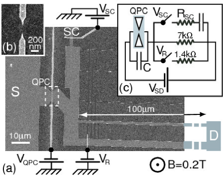
In this experiment, we have measured the variations in the resistance of a quantum point contact (QPC) realized in a 2D electron gas (2DEG) while changing the adjustable on-chip circuit in which it is embedded. The conduction channels of a QPC are directly related to the 1D sub-bands quantized by the transverse confinement GLAZMANetal1988 . By reducing the confinement with voltage biased top gates, the transmission probabilities of the conduction channels are increased continuously and, for adequate geometries BUTTIKER1990 , one channel at a time. Consequently, the QPC’s conductance corresponds to channels fully transmitted and one channel of transmission probability . The knowledge of the transmission probabilities combined with the ability to change them continuously make of a QPC a powerful test-bed for short coherent conductors REZNIKOVetal1995_KUMARetal1996 . As described later, we can change in-situ the circuit surrounding the QPC using voltage biased metallic top gates to deplete the 2DEG underneath. It is by monitoring the QPC’s resistance as a function of the circuit impedance that we can extract accurately the amplitude of DCB corrections.
The measured sample, shown in Fig. 1, was realized in a GaAs/Ga(Al)As heterojunction. The 2DEG is 94 nm deep, of density , Fermi energy K and mobility . The sample was patterned using e-beam lithography followed by chemical etching of the heterojunction and by deposition of metallic gates at the surface. The QPC is formed in the 2DEG by applying a negative voltage to the metallic split gates shown in Fig. 1(b). Two stripes of width m and m noteWEFF , and of length m, much longer than the electron phase coherence length m, were patterned in the 2DEG by chemical etching to form an on-chip resistance in series with the QPC. Measurements were performed in a dilution refrigerator of base temperature T mK. All measurement lines were filtered by commercial -filters at the top of the cryostat. At low temperature, the lines were carefully filtered and thermalized by arranging them as 1 m long resistive twisted pairs (m) inserted inside 260 m inner diameter CuNi tubes tightly wrapped around a copper plate screwed to the mixing chamber. The sample was further protected from spurious high energy photons by two shields, both at base temperature. Conductance measurements were performed using standard lock-in techniques at excitation frequencies below 100 Hz. The sample was current biased by a voltage source in series with a M or M polarization resistance at room temperature. Voltages across the sample were measured using low noise room temperature amplifiers. The source (S)-drain (D) voltage was kept smaller than to avoid heating. We applied a small perpendicular magnetic field B T noteB to minimize non-ideal behaviors of the QPC such as sharp energy dependence of the transmissions resulting from Fabry-Pérot resonances with nearby defects, and imperfect transmissions across “open” channels.
In our experiment the QPC is embedded in an electromagnetic environment schematically represented as a R//C circuit in Fig. 1(c). The parallel capacitance () is the geometrical capacitance between the source electrode (S) and the vertical near rectangular conductor on the right side of the QPC. If the short circuit electrode (SC) is disconnected ( V), the on-chip series resistance can take two values and depending on whether the wider 2DEG stripe is, respectively, connected () or disconnected ( V), using the metal gate voltage as a switch. If the SC electrode is connected (), it acts as a low impedance () high frequency path to ground in parallel with . Note that DCB reduces the DC conductance of a coherent conductor but that these DCB corrections depend on the impedance of the electromagnetic environment at high frequencies, typically GHz for mK. Consequently, while the SC electrode is connected at room temperature to a high input impedance voltage amplifier, at high frequencies the environment impedance is expected to be reduced to the on-chip resistance of the SC electrode plus, approximately, the vacuum impedance due to antenna effects on length scales larger than a fourth of the electromagnetic wavelength. This is symbolized in Fig. 1(c) by a high frequency impedance in series with a capacitor that acts as a high frequency short circuit.
The experiment was performed as follows: i) We first selected a series resistance or with . ii) With the short circuit electrode (SC) connected (), we tuned the QPC with . In this configuration the DCB corrections are minimum because the series resistance is shorted at high frequency by . Since the SC electrode is disconnected from ground at the near DC frequencies applied to measure the sample, it could be used to measure separately the QPC and the series resistances. iii) We then disconnected the SC electrode by applying a negative voltage , therefore increasing the high frequency circuit impedance and consequently the DCB corrections. By simultaneously measuring the variations of the source (S)-drain (D) resistance, which is the sum of the QPC and the series resistance, we can extract the amplitude of DCB corrections.
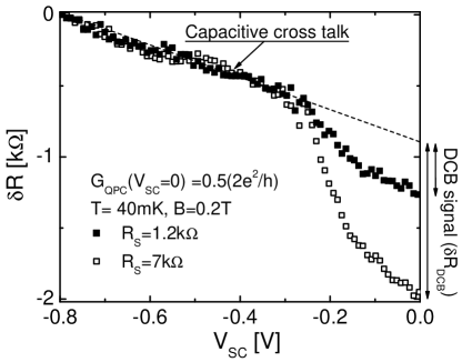
Figure 2 shows , the resistance variation of the QPC plus the series resistance from their values at V, plotted versus at , T mK and B T for and . The dependence of with results from two contributions: i) At V the SC electrode is disconnected and is a linear function of with a negative slope that does not depend on . This is a consequence of the capacitive cross talk between the metal gate controlled by and the QPC. We have checked (data not shown) that this slope, which is a non monotonous function of , is proportional to the derivative of the QPC’s resistance with . The normalization factor is in rough quantitative agreement with the sample geometry. ii) For V we observe, on top of the linear capacitive cross talk, a sudden drop when increases. We attribute this resistance drop, written hereafter , to the reduction of DCB corrections as the parallel high frequency short circuit electrode SC gets connected. As expected, is larger in the more resistive environment . In the following we extract by measuring the QPC in series with successively at V (SC electrode connected) and V (SC electrode disconnected). We then subtract the capacitive cross talk contribution obtained from V V.
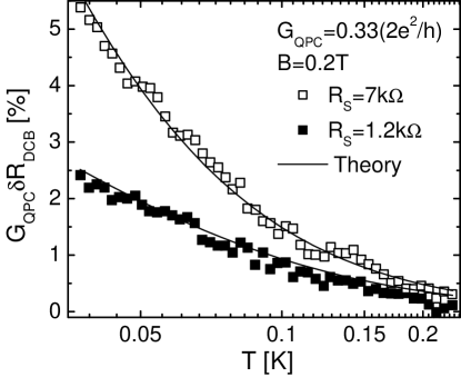
Figure 3 shows as symbols the measured temperature dependence of the DCB signal at for k and k. The continuous lines are predictions of the DCB theory for tunnel junctions SCT , normalized by the one-channel Fano factor . The schematic R//C circuit modeling the QPC’s electromagnetic environment is shown in Fig. 1(c). The real part of its impedance plugged into the theory reads . The calculated is the difference in the amplitude of DCB corrections for open and closed short circuit switch. The corresponding circuit resistance is, respectively, and . The only fit parameter in our calculation is the SC high frequency impedance that we fixed at k, in agreement with the sum of the on-chip SC resistance estimated from the geometry to 600 and the vacuum impedance 377 . Other parameters plugged into the DCB calculation are the measured series resistances k or k and the geometrical capacitance fF estimated numerically with an accuracy of fF noteCNUMERICAL . The very good agreement between data and theoretical predictions provides a strong support to our interpretation and allows us to now compare the measured dependence of DCB on transmission probabilities with the predicted Fano reduction factor.
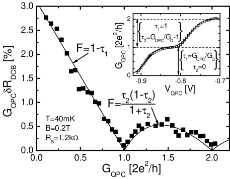
To test the generalized dynamical Coulomb blockade theory, we measured the relative amplitude of DCB corrections versus the QPC conductance at 40 mK and for k noteUCF (see Fig. 4). The predictions depend on the set , it is therefore crucial to extract accurately the transmissions probabilities of the QPC. The inset in Fig. 4 shows the QPC conductance up to versus the split gate voltage , measured at T=40 mK and B=0.2 T. We subtracted 350 from the data to account for the residual DC series resistance by adjusting the first three plateaus on multiples of the conductance quantum noteGQPC . From the maximum deviation between our data and the best fit (continuous line in inset of Fig. 4) using Büttiker’s model of QPCs BUTTIKER1990 , we estimate our accuracy on the transmission probabilities to be better than 0.05. The continuous line in Fig. 4 shows the relative amplitude of DCB as predicted by theory GZ2001_LEVYYEYATIetal2001 . We observe an excellent quantitative agreement between the data and the Fano factor that controls quantum shot noise REZNIKOVetal1995_KUMARetal1996 .
To conclude, we have performed a quantitative experimental test of the generalization of dynamical Coulomb blockade theory to short coherent conductors embedded in low impedance circuits. We find dynamical Coulomb blockade corrections that are reduced in amplitude by the same Fano factor as quantum shot noise, in quantitative agreement with the predictions. This result is not only important within the fundamental field of quantum electrodynamics in mesoscopic circuits. It also provides solid grounds to engineer complex devices with coherent conductors and to use dynamical Coulomb blockade as a tool to probe the transport mechanisms. For this purpose DCB has the advantage on shot noise that the signal increases when the probed energies decrease.
The authors gratefully acknowledge inspiring discussions and suggestions by D. Estève, P. Joyez, H. Pothier and C. Urbina. We also thank M.H. Devoret, F. Portier and B. Reulet for stimulating discussions and G. Faini, R. Giraud and Y. Jin for permanent assistance. This work was supported by the ANR (ANR-05-NANO-039-03) and NanoSci-ERA (ANR-06-NSCI-001).
References
- (1) M.H. Devoret et al., Phys. Rev. Lett. 64, 1824 (1990); S.M. Girvin et al., Phys. Rev. Lett. 64, 3183 (1990).
- (2) A.N. Cleland et al., Phys. Rev. B 45, 2950 (1992); T. Holst et al., Phys. Rev. Lett. 73, 3455 (1994).
- (3) For a review see G.-L. Ingold and Y.V. Nazarov, in Single Charge Tunneling, edited by H. Grabert and M.H. Devoret (Plenum, New York, 1992), Chap. 2.
- (4) P. Joyez et al., Phys. Rev. Lett. 80, 1956 (1998).
- (5) F. Pierre et al., Phys. Rev. Lett. 86, 1590 (2001).
- (6) D.S. Golubev and A.D. Zaikin, Phys. Rev. Lett. 86, 4887 (2001); A. Levy Yeyati et al., Phys. Rev. Lett. 87, 046802 (2001).
- (7) Th. Martin and R. Landauer, Phys. Rev. B 45, 1742 (1992).
- (8) M. Büttiker and R. Landauer, IBM J. Res. Dev. 30, 451 (1986).
- (9) See Y.M. Blanter and M. Büttiker, Phys. Rep. 336, 1 (2000) and references therein.
- (10) D. Pines and P. Nozière, The Theory of Quantum Liquids (W.A. Benjamin, New York, 1966); For a recent review on phase coherence of electrons in diffusive metals see F. Pierre et al., Phys. Rev. B 68, 085413 (2003).
- (11) A.V. Galaktionov et al., Phys. Rev. B 68, 085317 (2003); M. Kindermann and Y.V. Nazarov, Phys. Rev. Lett. 91, 136802 (2003); M. Kindermann et al., Phys. Rev. B 69, 035336 (2004); I. Safi and H. Saleur, Phys. Rev. Lett. 93, 126602 (2004).
- (12) R. Cron et al., in Electronic Correlations: From Meso to Nano-Physics, edited by T. Martin, G. Montambaux, and J. Trân Thanh Vân (EDP Sciences, Les Ulis, 2001), p. 17; R. Cron, PhD Thesis (available on http://tel.ccsd.cnrs.fr/), Université Paris 6 (2001).
- (13) L.I. Glazman et al., JETP Lett. 48, 238 (1988).
- (14) M. Büttiker, Phys. Rev. B 41, 7906 (1990).
- (15) M. Reznikov et al., Phys. Rev. Lett. 75, 3340 (1995); A. Kumar et al., Phys. Rev. Lett. 76, 2778 (1996).
- (16) The 2DEG width is about 700 nm narrower due to lateral depletion near the edges.
- (17) Shubnikov-de Haas oscillations of (B) are negligible up to the applied magnetic field B=0.2 T.
- (18) The code was provided gracefully by D. Estève.
- (19) For k and , non negligible universal conductance fluctuations of forbade us to extract the DCB signal accurately.
- (20) The corresponding reduction of is at most 2.5% and 5% below, respectively, the first and second plateau.